IEPC EPC9060 User manual

Development Board
EPC9060/61
Quick Start Guide
Half-bridge with Gate Drive
for EPC2030/31
Revision 2.0
QUICK START GUIDE
EPC – THE LEADER IN GaN TECHNOLOGY | WWW.EPC-CO.COM | COPYRIGHT 2019 | | 2
EPC9060/61
Table 1: Performance Summary (TA= 25 °C) EPC9060/61
Symbol Parameter Conditions Min Max Units
VDD Gate Drive Input Supply Range 7 12 V
VIN Bus Input Voltage Range
When using 40 V devices, EPC9060 32(1) V
When using 60 V devices, EPC9061 48(1) V
VOUT Switch Node Output Voltage
When using 40 V devices, EPC9060 40 V
When using 60 V devices, EPC9061 60 V
IOUT Switch Node Output Current
When using 40 V devices, EPC9060 25(1) A
When using 60 V devices, EPC9061 24(1) A
VPWM PWM Logic Input Voltage Threshold Input ‘Low’ 3.5 6 V
Input ‘High’ 0 1.5 V
Minimum “High” State Input Pulse Width VPWM rise and fall time < 10ns 50 ns
Minimum “Low” State Input Pulse Width VPWM rise and fall time < 10ns 100(2) ns
(1)
Assumes inductive load, maximum current depends on die temperature – actual maximum current with be subject to switching frequency,
bus voltage and thermal cooling.
(2)
Limited by time needed to‘refresh’high side bootstrap supply voltage.
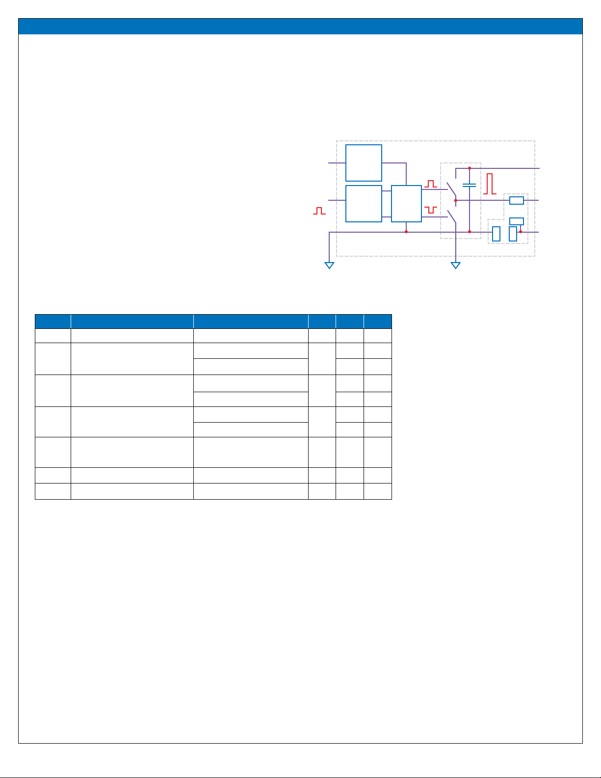
Figure 1: Block Diagram of Development Board
VDD VIN
PWM
input
OUT
VSW
Gate drive supply
Pads for buck output lter
Half bridge
with bypass
Logic and
dead-time
adjust
Gate drive
regulator
LM5113
gate
driver
DESCRIPTION
These development boards are in a half-bridge topology with onboard
gate drives, featuring the EPC2030/31 eGaN® eld eect transistors
(FETs). The purpose of these development boards is to simplify the
evaluation process of these eGaN FETs by including all the critical
components on a single board that can be easily connected into any
existing converter.
The development board is 2” x 2” and contains two eGaN FETs in a
half-bridge conguration using the Texas Instruments LM5113 gate
driver, supply and bypass capacitors. The board contains all critical
components and layout for optimal switching performance and has
additional area to add buck output lter components on the board.
There are also various probe points to facilitate simple waveform
measurement and eciency calculation. A complete block diagram of
the circuit is given in gure 1.
For more information on the EPC2030 and EPC2031 eGaN FETs, please
refer to the datasheets available from EPC at www.epc-co.com. The
datasheet should be read in conjunction with this quick start guide.

QUICK START GUIDE
EPC – THE LEADER IN GaN TECHNOLOGY | WWW.EPC-CO.COM | COPYRIGHT 2019 | | 3
EPC9060/61
Figure 2: Proper Connection and Measurement Setup
Figure 3: Proper Measurement of Switch Node – OUT
Place probe tip inlarge via at OUT
Ground probe
against TP3
Minimize loop
Do not use probe ground lead
QUICK START PROCEDURE
The development boards are easy to set up to evaluate the performance
of the eGaN FET. Refer to gure 2 for proper connect and measurement
setup and follow the procedure below:
1. With power o, connect the input power supply bus to +VIN
(J5, J6) and ground / return to –VIN (J7, J8).
2. With power o, connect the switch node of the half-bridge OUT
(J3, J4) to your circuit as required.
3. With power o, connect the gate drive input to +VDD (J1, Pin-1)
and ground return to –VDD (J1, Pin-2).
4. With power o, connect the input PWM control signal to PWM
(J2, Pin-1) and ground return to any of the remaining J2 pins.
5. Turn on the gate drive supply – make sure the supply is between
7 V and 12 V range.
6. Turn on the bus voltage to the required value (do not exceed the
absolute maximum voltage on VOUT as indicated in the table be-
low:
a. EPC9060, 40 V
b. EPC9061, 60 V
7. Turn on the controller / PWM input source and probe switching
node to see switching operation.
8. Once operational, adjust the bus voltage and load PWM control
within the operating range and observe the output switching
behavior, eciency and other parameters.
9. For shutdown, please follow steps in reverse.
NOTE. When measuring the high frequency content switch node (OUT), care must be
taken to avoid long ground leads. Measure the switch node (OUT) by placing the oscil-
loscope probe tip through the large via on the switch node (designed for this purpose)
and grounding the probe directly across the GND terminals provided. See gure 3 for
proper scope probe technique.
(For Eciency
Measurement)
Gate Drive Supply
(Note Polarity)
+
7 V – 12 V
+
_
PWM Input
+
VDD Supply
VIN Supply
V
IN
(For Eciency
Measurement)
Pads for Buck
Output Filter
VOUT
VSW
PGND
+
VOUT
V
A
IIN
_
_
_
V
See table
for max
QUICK START GUIDE
EPC – THE LEADER IN GaN TECHNOLOGY | WWW.EPC-CO.COM | COPYRIGHT 2019 | | 4
EPC9060/61
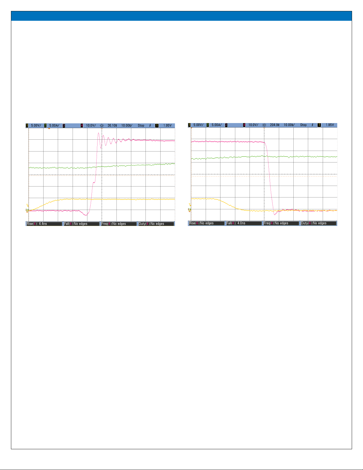
!
Typical Waveforms forVIN = 60V to 5V/20 A (300 kHz) Buck converter CH1: (VPWM) Input logic signal – CH2: (IOUT) Output inductor current – CH4: (VOUT) Switch node voltage
Figure 4 (a) – Rising Edge Figure 4 (b) – Falling Edge
THERMAL CONSIDERATIONS
The EPC9060/61 development boards showcase the EPC2030/31
eGaN FETs. Although the electrical performance surpasses that for
traditional Silicon devices, their relatively smaller size does magnify
the thermal management requirements. These development boards
are intended for bench evaluation with low ambient temperature and
convection cooling. The addition of heat-sinking and forced air cooling
can signicantly increase the current rating of these devices, but care
must be taken to not exceed the absolute maximum die temperature
of 150°C.
NOTE. The EPC9060/61 development boards do not have any current or thermal
protection on board.

QUICK START GUIDE
EPC – THE LEADER IN GaN TECHNOLOGY | WWW.EPC-CO.COM | COPYRIGHT 2019 | | 5
EPC9060/61
Table 2 : Bill of Material
Item Qty Reference Part Description Manufacturer Part Number
1 3 C4, C10, C11 Capacitor, 1 µF, 10%, 25 V, X5R Murata GRM188R61E105KA12D
2 2 C16, C17 Capacitor, 100 pF, 5%, 50 V, NP0 Kemet C0402C101K5GACTU
3 1 C9 Capacitor, 0.1 µF, 10%, 25 V, X5R TDK C1005X5R1E104K
4 1 C19 Capacitor, 1 µF, 10%, 25 V, X5R C1005X5R1E105K
5 4 C21, C22, C23, C24 Capacitor, - see Table 3 See Table 3
6 2 D1, D2 Schottky Diode, 30 V Diodes Inc. SDM03U40-7
7 3 J1, J2, J9 Connector FCI 68001-236HLF
8 1 J3, J4, J5, J6, J7, J8 Connector FCI 68602-224HLF
9 2 Q1, Q2 eGaN® FET - see Table 3 See Table 3
10 1 R1 Resistor, 10.0 k, 5%, 1/10 W Panasonic ERJ-3GEY0R00V
11 2 R2, R15 Resistor, 0 Ω, 1/8 W Stackpole RMCF0603ZT0R00
12 1 R4 Resistor, 47 Ω, 1%, 1/10 W Stackpole RMFC0603FT47R0
13 1 R5 Resistor, 75 Ω, 1%, 1.10 W Stackpole RMCF0603FT75R0
14 4 R19, R20, R23, R24 Resistor, 0 Ω, 1/16 W Stackpole RMCF0402ZT0R00
15 2 TP1, TP2 Test Point Keystone Elect 5015
16 1 TP3 Connector 1/40th of Tyco 4-103185-0
17 1 U1 I.C., Logic Fairchild NC7SZ00L6X
18 1 U2 I.C., Gate Driver National LM5113
19 1 U3 I.C., Regulator Microchip MCP1703T-5002E/MC
20 1 U4 I.C., Logic Fairchild NC7SZ08L6X
21 0 R14 Optional Resistor
22 0 D3 Optional Diode
23 0 P1, P2 Optional Potentiometer
Table 3 : Variable BOM Components
Board Number Item Qty Reference Part Description Manufacturer Part Number
EPC9060
5 4 C21, C22, C23, C24 Capacitor, 4.7 µF, 50 V ±10%, X5R TDK C2012X5R1H475K125AB
9 2 Q1, Q2 eGaN® FET EPC EPC2030
EPC9061
5 4 C21, C22, C23, C24 Capacitor, 1 µF, 100 V ±10%, X7S TDK CGA4J3X7S2A105K125AE
9 2 Q1, Q2 eGaN® FET EPC EPC2031

QUICK START GUIDE
EPC – THE LEADER IN GaN TECHNOLOGY | WWW.EPC-CO.COM | COPYRIGHT 2019 | | 6
EPC9060/61
VCC
7 - 12 Vdc
C4
1µF, 25V
C10
1µF, 25V
1
2
J1
CON2
R1
10k
PWM1
GND
A
B
Y
VDD
U1
NC7SZ00L6X
See Table
SW OUT
GND
1
TP3
CON1
1
2
3
4
J8
CON4
1
2
3
4
J7
CON4
1
2
3
4
J3
CON4
1
2
3
4
J4
CON4
1
2
3
4
J6
CON4
1
2
3
4
J5
CON4
C11
1µF, 25V
1
TP2
Keystone 5015
1
TP1
Keystone 5015
R2
Zero
R14
Optional
R15
Zero
R5
75
D2
SDM03U40
R4
47
D1
SDM03U40
PWM2
VCC
OUT 1
NC 2
NC 3
GND 4
NC
5
NC
6
NC
7
IN
8
GND
9
U3 MCP1703
1
2
J2
CON2
1
2
J9
CON2
2
P1
Optional
2
P2
Optional
GND
A
B
Y
VDD
U4
NC7SZ08L6X C9
0.1µF, 25V
R19 Zero
R20 Zero
R23 Zero
R24 Zero
C22
C23
C21
U2
LM5113TM
C19
0.1µF, 25V
C17
100pF
C16
100pF
D3
Optional
Q1
See Table
Q2
See Table
C24
See Table
Figure 5: Development Board Schematic

EPC Products are distributed through Digi-Key.
www.digikey.com
For More Information:
or your local sales representative
Visit our website:
www.epc-co.com
Sign-up to receive
EPC updates at
bit.ly/EPCupdates
or text“EPC”to 22828
Demonstration Board Notication
The EPC9060/61 board is intended for product evaluation purposes only. It is not intended for commercial use nor is it FCC approved for resale. Replace components on
the Evaluation Board only with those parts shown on the parts list (or Bill of Materials) in the Quick Start Guide. Contact an authorized EPC representative with any questions.This board is
intended to be used by certied professionals, in a lab environment, following proper safety procedures. Use at your own risk.
As an evaluation tool, this board is not designed for compliance with the European Union directive on electromagnetic compatibility or any other such directives or regulations. As board
buildsare at timessubject to productavailability,it ispossible thatboardsmaycontain components orassembly materialsthatarenot RoHScompliant.EcientPowerConversion Corpora-
tion (EPC) makes no guarantee that the purchased board is 100% RoHS compliant.
The Evaluation board (or kit) is for demonstration purposes only and neither the Board nor this Quick Start Guide constitute a sales contract or create any kind of warranty, whether express
or implied, as to the applications or products involved.
Disclaimer: EPC reserves theright at any time, without notice, to makechanges toany products described hereinto improvereliability, function, or design. EPCdoes not assumeany liability
arising out of the application or use of any product or circuit described herein; neither does it convey any license under its patent rights, or other intellectual property whatsoever, nor the
rights of others.
This manual suits for next models
1
Table of contents
Other IEPC Motherboard manuals


