IEPC EPC90132 User manual

Development Board
EPC90132
Quick Start Guide
40 V Half-bridge with Gate Drive, Using EPC2055
Revision 1.0
QUICK START GUIDE EPC90132
EPC – POWER CONVERSION TECHNOLOGY LEADER | EPC-CO.COM | ©2021 | | 2
DESCRIPTION
The EPC90132 is a half bridge development board with onboard gate
drives, featuring the 40 V rated EPC2055 GaN eld eect transistor (FET).
The purpose of this development board is to simplify the evaluation
process of the EPC2055 by including all the critical components on a
single board that can be easily connected into the majority of existing
converter topologies.
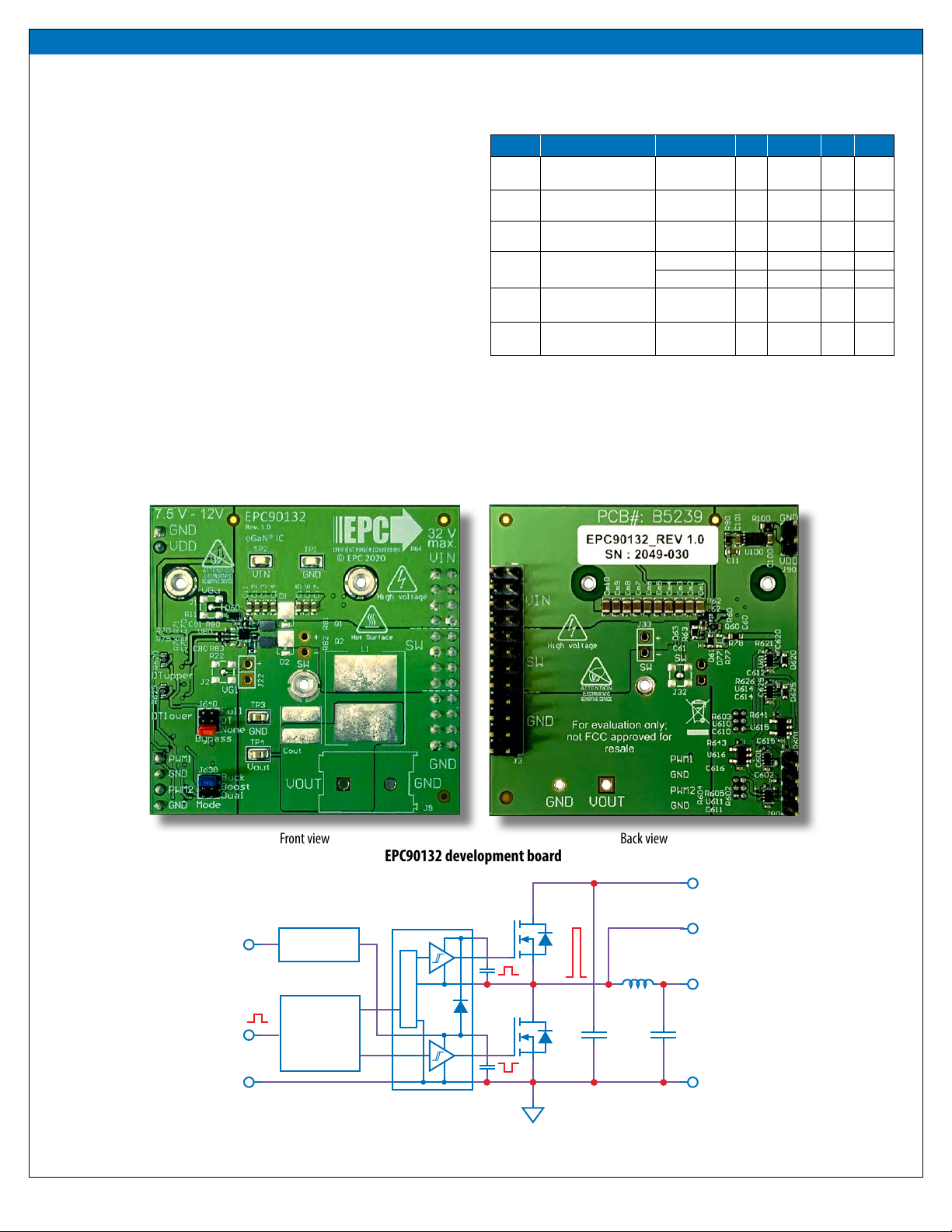
The EPC90132 development board measures 2” x 2” and contains two
EPC2055 GaN FET in a half bridge conguration and one EPC2038 GaN
FET used to augment the bootstrap supply. The EPC90132 features the uPI
Semiconductor uP1966A gate driver. The board also contains all critical
components and the layout supports optimal switching performance.
There are also various probe points to facilitate simple waveform
measurement and eciency calculation. A block diagram of the circuit
is given in gure 1.
For more information on EPC2055 please refer to their datasheets
available from EPC at www.epc-co.com. The datasheet should be read in
conjunction with this quick start guide.
Table 1: Performance Summary (TA= 25°C) EPC90132
Symbol Parameter Conditions Min Nominal Max Units
VDD
Gate Drive Regulator
Supply Range 7.5 12 V
VIN
Bus Input Voltage
Range(1) 32 V
IOUT
Switch Node Output
Current (2) 25 A
VPWM
PWM Logic Input
Voltage Threshold (3)
Input ‘High’ 3.5 5.5 V
Input ‘Low’ 0 1.5 V
PWM ‘High’State Input
Pulse Width
VPWM rise and
fall time < 10ns 50 ns
PWM ‘Low’ State Input
Pulse Width (4)
VPWM rise and
fall time < 10ns 200 ns
(1) Maximum input voltage depends on inductive loading, maximum switch node ringing
must be kept under 40 V for EPC2055.
(2) Maximum current depends on die temperature – actual maximum current is aected by
switching frequency, bus voltage and thermal cooling.
(3) When using the on board logic buers, refer to the uP1966A datasheet when bypassing
the logic buers.
(4) Limited by time needed to ‘refresh’ high side bootstrap supply voltage.
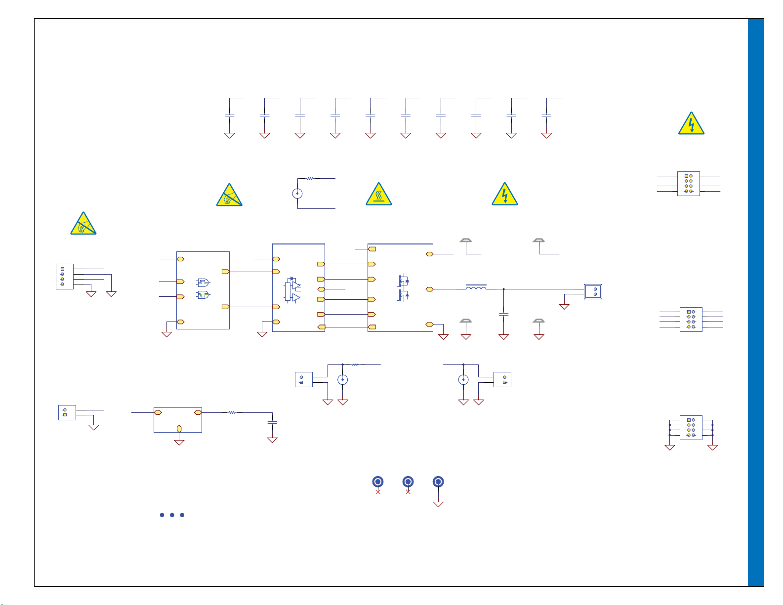
EPC90132 development board
Back viewFront view
Figure 1: Block diagram of EPC90132 development board default conguration
Level shift
VDD
VIN
Switch node
Q1
Q2
CBypass
PWM
GND
Cout
Gate drive
regulator
Gate driver
DC Output
PGND
Logic and
dead-time
adjust
L1
QUICK START GUIDE EPC90132
EPC – POWER CONVERSION TECHNOLOGY LEADER | EPC-CO.COM | ©2021 | | 3
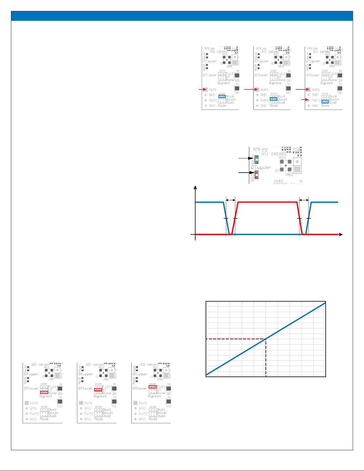
Figure 3: Denition of dead-time between the upper-FET gate signal (DTQup)
and the lower-FET gate signal (DTQlow)
Figure 4: The required resistance values for R620 or R625 as a
function of desired dead-time
Figure 2: Input mode selection on J630
(a) (c)(b)
QUICK START PROCEDURE
The EPC90132 development board is easy to set up as a buck or boost
converter to evaluate the performance of two EPC2055 eGaN FETs.
This board includes a logic PWM input signal polarity changer used to ensure
positive PWM polarity for the switching device when congured in either
the buck or boost modes, and can accommodate both single and dual PWM
inputs. Furthermore, the board includes a dead-time generating circuit that
adds a delay from when the gate signal of one FET is commanded to turn
o, to when the gate signal of the other FET is commanded to turn on. In the
default conguration, this dead time circuit ensures that both the high and
low side FETs will not be turned on at the same time thus preventing a shoot-
through condition. The dead-time and/or polarity changing circuits can be
utilized or bypassed for added versatility.
Single/dual PWM signal input settings
There are two PWM signal input ports on the board, PWM1 and PWM2. Both
input ports are used as inputs in dual-input mode where PWM1 connects to
the upper FET and PWM2 connects to the lower FET. The PWM1 input port
is used as the input in single-input mode where the circuit will generate
the required complementary PWM for the FETs. The input mode is set by
choosing the appropriate jumper positions for J630 (mode selection) as
shown in gure 2(a) for a single-input buck converter (blue jumper across
pins 1 & 2 of J630), (b) for a single-input boost converter (blue jumpers
across pins 3 & 4 of J630), and (c) for a dual-input operation (blue jumpers
across pins 5 & 6 of J630).
Note: In dual mode there is no shoot-through protection as both gate
signals can be set high at the same time.
Dead-time settings
Dead-time is dened as the time between when one FET turns o and the
other FET turns on, and for this board is referenced to the input of the gate
driver. The dead-time can be set to a specic value where resistor R620
delays the turn on of the upper FET and resistor R625 delays the turn on of
the lower FET as illustrated in gure 3.
The required resistance for the desired dead-time setting can be read o
the graph in gure 4. An example for 10 ns dead-time setting shows that
a 120 Ω resistor is needed.
Note: This is the default deadtime and resistor value installed. A minimum
dead-time of is 5 ns and maximum of 15 ns is recommended.
Bypass settings
Both the polarity changer and the deadtime circuits can be bypassed using
the jumper settings on J640 (Bypass), for direct access to the gate driver
input. There are three bypass options: 1) No bypass, 2) Dead-time bypass,
3) Full bypass. The jumper positions for J640 for all three bypass options are
shown in gure 5.
PWM1
Single input
Buck
Single input
Boost Dual input
PWM2
R(Ω) = 13.5 ∙ DT(ns) − 14
Resistance (Ω)
Dead-time (ns)
190
180
170
160
150
140
130
120
110
100
90
80
70
60
505 6 7 8 9 10 11 12 13 14 15
Figure 5: Bypass mode Jumper settings for J640
(a) (c)(b)
Deadtime
v
t
0
50% 50% 50% 50%
DTQup
DTQlow
Deadtime
Lower FET
turn on delay
Lower FET turn on delay
Upper FET
turn on delay
Upper FET turn on delay
No bypass Bypass deadtime Full Bypass

QUICK START GUIDE EPC90132
EPC – POWER CONVERSION TECHNOLOGY LEADER | EPC-CO.COM | ©2021 | | 4
In no-bypass mode, gure 5(a) (red jumper across pins 5 & 6 of
J640), both the on-board polarity and dead-time circuits are fully
utilized. In dead-time bypass mode, gure 5(b) (red jumpers
across pins 3 & 4 of J640), only the on-board polarity changer
circuit is utilized, eectively bypassing the dead-time circuit.
In full bypass mode, Figure 5(c) (red jumper across pins 1 & 2 of
J640), the inputs to the gate driver are directly connected to the
PWM1 and PWM2 pins and the on-board polarity and dead-time
circuits are not utilized.
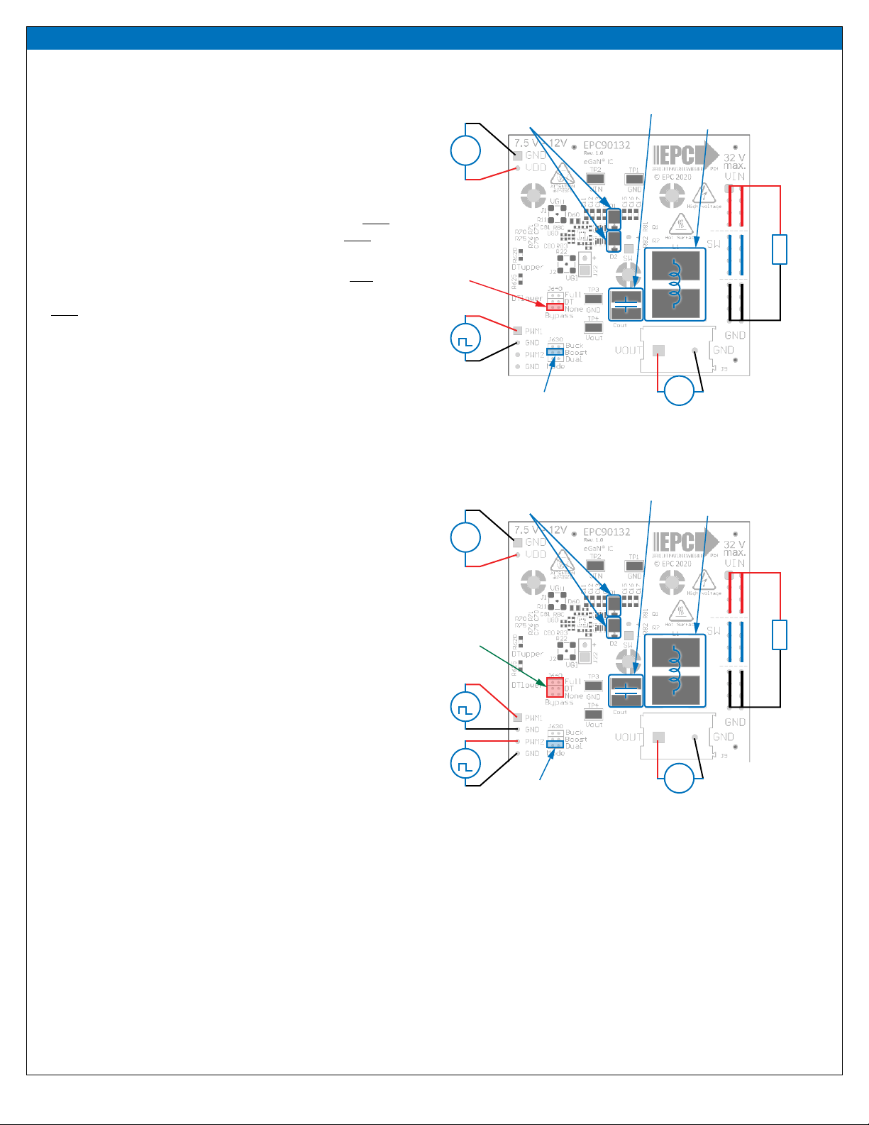
Buck converter conguration
To operate the board as a buck converter, either a single or dual
PWM inputs can be chosen using the appropriate jumper settings
on J630 (mode).
To select Single Input Buck Mode, the bypass jumper J640 must be
set to the no-bypass mode, the buck mode J630 must be selected
as shown in gure 6(a).
To select Dual Input Buck Mode, the bypass jumper J640 may be
congured to any of the valid settings, the dual-input mode J630
must be selected as shown in gure 6(b).
Note: It is important to provide the correct PWM signals that
includes dead-time and polarity when operating in bypass mode.
Once the input source, dead-time settings and bypass cong-
urations have be chosen and set, then the boards can be operated.
1. With power o, connect the input power supply bus to VIN and
ground / return to GND.
2. With power o, connect the switch node (SW) of the half bridge
to your circuit as required (half bridge conguration). Or use the
provided pads for inductor (L1) and output capacitors (Cout), as
shown in gure 6.
3. With power o, connect the gate drive supply to VDD (J1, Pin-1)
and ground return to GND (J1, Pin-2 indicated on the bottom
side of the board).
4. With power o, connect the input PWM control signal to PWM1
and/or PWM2 according to the input mode setting chosen and
ground return to any of GND J2 pins indicated on the bottom
side of the board.
5. Turn on the gate drive supply – make sure the supply is set
between 7.5 V and 12 V.
6. Turn on the controller / PWM input source.
7. Making sure the initial input supply voltage is 0 V, turn on the
power and slowly increase the voltage to the required value
(do not exceed the absolute maximum voltage). Probe switch-
node to see switching operation.
8. Once operational, adjust the PWM control, bus voltage, and load
within the operating range and observe the output switching
behavior, eciency, and other parameters.
9. For shutdown, please follow steps in reverse.
Bypass mode warnings
• It is important to provide the correct PWM signals that includes dead-
time and polarity for either buck or boost operation when making use
of bypass modes.
• When operating in full bypass mode, the input signal specications
revert to that of the uP1966A gate driver IC. Refer to the uP1966A
datasheet for details.
32 VDCmax
VDD supply
(Note polarity)
Output Capacitor
Output Inductor
PWM1
(default)
Jumper positions for
single-input buck
Optional anti-
parallel diodes
DC load
Switch-node
output
Must be in
No-bypass
position
+
+
+
Output Capacitor
Output Inductor
Optional anti-
parallel diodes
7.5 –12 VDC
32 VDCmax
VDD supply
(Note polarity)
VMain
supply
(Note
polarity)
VMain
supply
(Note
polarity)
PWM1
Upper
FET
PWM2
Lower
FET DC load
All valid
positions
permitted
+
+
+
+
7.5 –12 VDC
Jumper positions for
dual-input buck
(a)
(b)
Figure 6: (a) Single-PWM input buck converter (b) Dual-PWM input buck converter
congurations showing the supply, anti-parallel diodes, output capacitor,
inductor, PWM, and load connections with corresponding jumper positions.
QUICK START GUIDE EPC90132
EPC – POWER CONVERSION TECHNOLOGY LEADER | EPC-CO.COM | ©2021 | | 5
Boost Converter conguration
Warning: Never operate the boost converter mode without a
load, as the output voltage can increase beyond the maximum
ratings.
To operate the board as a boost converter, either a single or dual
PWM inputs can be chosen using the appropriate jumper settings
on J630 (mode).
To select Single Input Boost Mode, the bypass jumper J640 must
be set to the no-bypass mode, the boost mode J630 must be
selected as shown in gure.7(a).
To select Dual Input Boost Mode, the bypass jumper J640 may be
congured to any of the valid settings, the dual-input mode J630
must be selected as shown in gure 7(b).
Note: It is important to provide the correct PWM signals that
includes dead-time and polarity when operating in bypass mode.
Once the input source, dead-time settings and bypass congura-
tions have be chosen and set, then the boards can be operated.
1. The inductor (L1) and input capacitors (labeled as Cout) can
either be soldered onto the board, as shown in gure 7, or
provided o board. Anti-parallel diodes can also be installed
using the additional pads on the right side of the EPC2055 FETs.
2. With power o, connect the input power supply bus to VOUT
and ground / return to GND, or externally across the capacitor
if the inductor L1 and Cout are provided externally. Connect the
output voltage (labeled as VIN) to your circuit as required, e.g.,
resistive load.
3. With power o, connect the gate drive supply to VDD (J1, Pin-1)
and ground return to GND (J1, Pin-2 indicated on the bottom
side of the board).
4. With power o, connect the input PWM control signal to PWM1
and/or PWM2 according to the input mode setting chosen and
ground return to any of GND J2 pins indicated on the bottom
side of the board.
5. Turn on the gate drive supply – make sure the supply is between
7.5 V and 12 V.
6. Turn on the controller / PWM input source.
7. Making sure the output is not open circuit, and the input
supply voltage is initially 0 V, turn on the power and slowly
increase the voltage to the required value (do not exceed
the absolute maximum voltage). Probe switch-node to see
switching operation.
8. Once operational, adjust the PWM control, bus voltage, and load
within the operating range and observe the output switching
behavior, eciency, and other parameters. Observe device
temperature for operational limits.
9. For shutdown, please follow steps in reverse.
VDD supply
(Note polarity)
Output Capacitor
Output Inductor
PWM1
(default)
Optional anti-
parallel diodes
Must be in
No-bypass
position
+
+
7.5 –12 VDC
32 VDCmax
DC load
+
VMain supply
(Note polarity)
32 VDCmax
DC load
Output Capacitor
Output Inductor
Optional anti-
parallel diodes
7.5 –12 VDC
VDD supply
(Note polarity)
PWM1
Upper
FET
PWM2
Lower
FET
All valid
positions
permitted
+
+
+
+
VMain supply
(Note polarity)
Jumper positions for
single-input boost
Jumper positions for
dual-input boost
(a)
(b)
Figure 7: (a) Single-PWM input boost converter (b) Dual-PWM input boost
converter congurations showing the supply, inductor, anti-parallel diodes, output
capacitor, PWM, and load connections with corresponding jumper settings.
QUICK START GUIDE EPC90132
EPC – POWER CONVERSION TECHNOLOGY LEADER | EPC-CO.COM | ©2021 | | 6
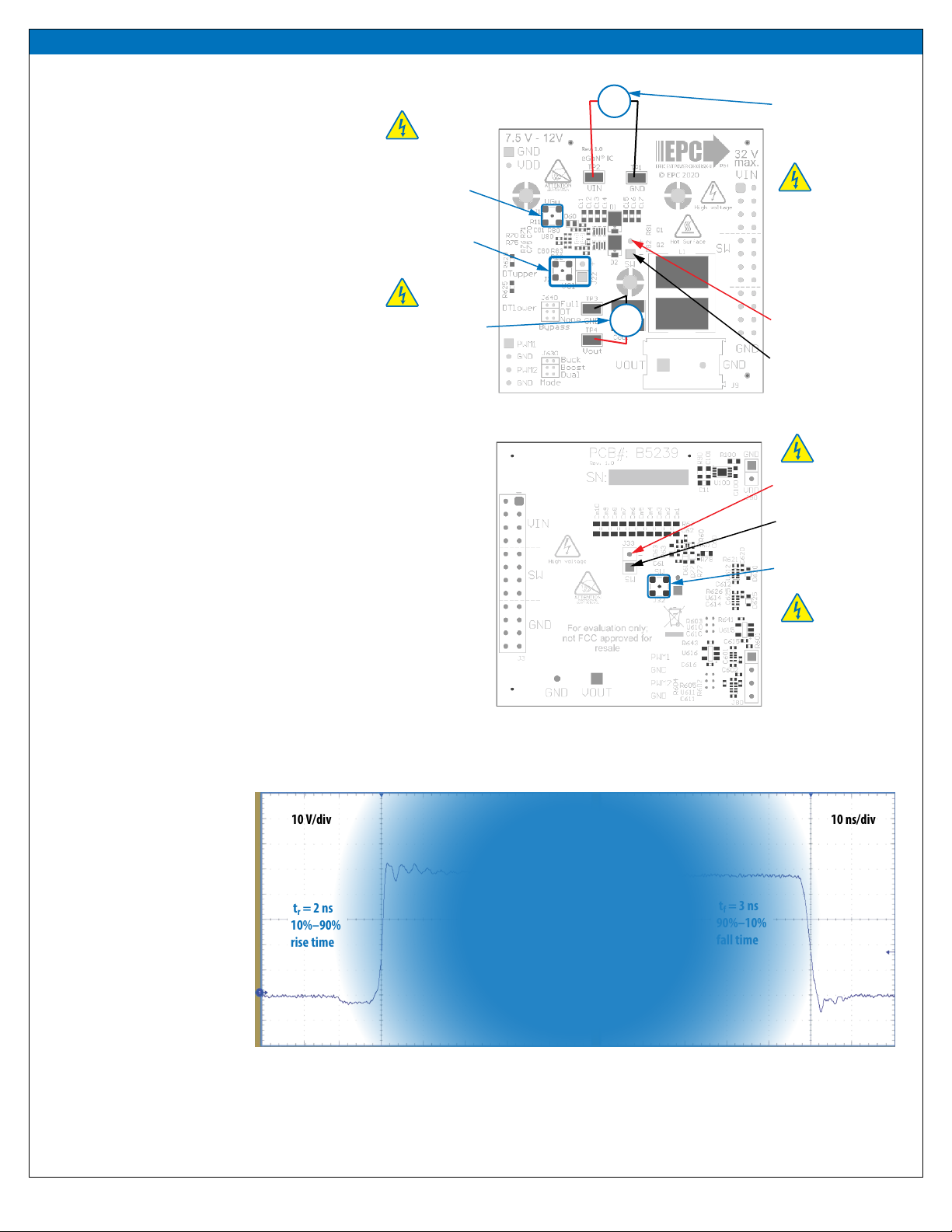
Ground oscilloscope probe
Switch-node oscilloscope
probe (HIGH VOLTAGE!)
Switch-node MMCX
(HIGH VOLTAGE!)
HIGH VOLTAGE
HIGH VOLTAGE
(a)
(b)
Figure 8: Measurement points (a) top side, (b) bottom side
Figure 9: Typical switch-node waveform when operated as a buck converter
MEASUREMENT CONSIDERATIONS
Measurement connections are shown in gure 8.
Figure 9 shows an actual switch-node voltage
measurement when operating the board as a buck
converter.
When measuring the switch node voltage containing
high-frequency content,caremustbe takentoprovide
an accurate high-speed measurement. An optional
two pin header (J33) and an MMCX connector (J32)
are provided for switch-node measurement.
A dierential probe is recommended for measuring
the high-side bootstrap voltage. IsoVu probes from
Tektronix has a mating MMCX connector.
For regular passive voltage probes (e.g. TPP1000)
measuring switch node using MMCX connector,
probe adaptor is available. PN: 206-0663-xx.
NOTE. For information about measurement techniques,
the EPC website oers: “AN023 Accurately Measuring
High Speed GaN Transistors” and the How to GaN
educational video series,including: HTG09- Measurement
EPC90132
Lower FET
Gate Voltage
Ground oscilloscope probe
Switch-node
oscilloscope probe
V
V
+
+
Upper FET Gate
Voltage MMCX
(HIGH VOLTAGE!)
Voltage measurement:
Input voltage for Buck,
Output voltage for Boost
(HIGH VOLTAGE!)
Voltage measurement:
Input voltage for Boost,
Output voltage for Buck
(HIGH VOLTAGE!)
HIGH VOLTAGE
HIGH VOLTAGE
HIGH VOLTAGE
V
IN
= 48 V, V
OUT
= 12 V, I
OUT
= 20 A, f
sw
= 1 MHz, L = 2.2 μH
10 V/div 10 ns/div
t
f
= 3 ns
90%–10%
fall time
t
r
= 2 ns
10%–90%
rise time
Waiting on update

QUICK START GUIDE EPC90132
EPC – POWER CONVERSION TECHNOLOGY LEADER | EPC-CO.COM | ©2021 | | 7
Components to remove prior
to Heat-spreader attach
Spacers for heat-spreader
attach
M2 screws (x3)
20 mm 9.2 mm
16.7 mm
Heat-spreader
Insulator
PCB
assembly
SMD spacer (x3)
eGaN FETs (x2)
TIM
Figure 10: Details for attaching a heatsink to the EPC90132 board.
(a) 3D perspective, (b) top view details.
THERMAL CONSIDERATIONS
The EPC90132 is intended for bench evaluation
with low ambient temperature and convection
cooling. The addition of a heat-spreader or heatsink
and forced air cooling can signicantly increase
the current rating of these devices, but care must
be taken to not exceed the absolute maximum die
temperature of 150°C.
The EPC90132 board is equipped with three
mechanical spacers that can be used to easily
attach a heat-spreader or heatsink as shown in
gure 10 (a), and only requires a thermal interface
material (TIM), a custom shape heat-spreader/
heatsink, and screws. Prior to attaching a heat-
spreader, any component exceeding 1 mm in
thickness under the heat-spreader area will need
to be removed from the board as shown in gure
10 (b). When assembling the heatsink, it may
be necessary add a thin insulation layer for
components with expose conductors such as
capacitors and resistors.
The choice of TIM needs to consider the following
characteristics:
• Mechanical compliance – The TIM becomes
compressed during heatsink attached and exerts
a force on the FETs. A maximum compression of
2:1 is recommended for maximum thermal perfor-
mance and to constrain the mechanical force that
maximizes thermal mechanical reliability.
• Electrical insulation – The backside of the eGaN
FETs are substrate that are connected to source
and the upper FET will thus be connected to the
switch-node. The TIM must therefore provide
insulation to prevent short-circuiting the upper
FET to the ground.
• Thermal performance – The choice of thermal
material will aect the thermal performance.
Higher thermal conductivity materials will result in
higher thermal performance.
EPC recommends t-Global P/N: TG-X 500 µm for
the thermal interface material.
The mechanical spacers will accept M2 x 0.4 mm
thread screws.
NOTE. The EPC90132 development board does not have
any current or thermal protection on board. For more
information regarding the thermal performance of EPC
eGaN FETs, please consult:
D. Reusch and J. Glaser, DC-DC Converter Handbook,
a supplement to GaN Transistors for Ecient
Power Conversion, First Edition, Power Conversion
Publications, 2015.
(a)
(b)

QUICK START GUIDE EPC90132
EPC – POWER CONVERSION TECHNOLOGY LEADER | EPC-CO.COM | ©2021 | | 8
QUICK START GUIDE EPC90132
Table 2: Bill of Materials
Item Qty Reference Part Description Manufacturer Part Number
1 1 C11 1 μF TDK C1608X7R1E105K080AB
2 9 C60, C61, C81, C610, C611, C612, C614, C615, C616 0.1 μF, 25 V Yageo CC0402KRX7R8BB104
3 1 C62 22 nF, 25 V TDK C1005X7R1E223K050BB
4 1 C80 4.7 μF, 10 V TDK C1005X5R1A475K050BC
5 2 C100, C101 1 μF, 25 V TDK C1608X7R1E105K
6 2 C601, C602 47 pF, 50 V Yegeo CC0402JRNPO9BN470
7 2 C620, C625 100 pF, 50 V Yegeo CC0402KRX7R9BB101
8 7 Ci1, Ci2, Ci3, Ci4, Ci5, Ci6, Ci7 1 μF, 50 V Taiyo Yuden UMK107AB7105KA-T
910 Cm1, Cm2, Cm3, Cm4, Cm5, Cm6, Cm7, Cm8, Cm9, Cm10 4.7 μF, 50 V TDK C2012X7R1H475K125AC
10 1D60 5 V1, 150 mW Bournes CD0603-Z5V1
11 4D61, D63, D620, D625 40 V 30 mA Diodes Inc. SDM03U40
12 1J3 100 mil 2x12 male header Amphenol 68602-224HLF
13 1J80 100 mil 1x4 male header Tyco 4-103185-0-04
14 1 J90 100 mil 1x2 male header Tyco 4-103185-0-02
15 2J630, J640 .05" Dual Row Male 3-Pos Vert. Sullins GRPB032VWVN-RC
16 1JP630 50 mil +Handle Blue Harwin Inc M50-2030005
17 1JP640 50 mil +Handle Red Harwin Inc M50-2020005
18 2Q1, Q2 40 V 32 A 3.5 mΩ EPC EPC2055
19 1Q60 100 V 2800 mΩ EPC EPC2038
20 1R62 27 k Panasonic ERJ-2GEJ273X
21 1R63 20 Ω Stackpole RMCF0402JT20R0
22 2 R70, R75 2.2 Ω Panasonic ERJ-2GEJ2R2X
23 11 R71, R76, R601, R602, R603, R604, R605, R621, R626, R641, R643 10 k Yageo RC0402FR-0710KL
24 3 R77, R81, R83 0 Ω Stackpole RMCF0402ZT0R00
25 3 R78, R90, R100 0 Ω Panasonic ERJ-3GEY0R00V
26 2R80, R82 1 Ω Yageo RC0402FR-071RL
27 2R620, R625 120 Ω 1% Yageo RC0603FR- 07120RL
28 3 SO1, SO2, SO3 M2 SMD spacer Wurth 9774010243R
29 4 TP1, TP2, TP3, TP4 Test point Keystone 5015
30 1U80 100 V eGaN Driver uPI uP1966A
31 1U100 5.0 V 250 mA DFN Microchip MCP1703T-5002E/MC
32 4U610, U611, U612, U614 Recong Logic Nexperia 74LVC1G99G
33 2U615, U616 Bilateral Analog Switch Texas Instruments SN74LVC1G66DBV
Optional Components
Item Qty Reference Part Description Manufacturer Part Number
1 2 C70, C75 100 pF, 50 V Yegeo CC0402KRX7R9BB101
2 1 Cout GenericOutputCap TBD TBD
3 2 D1, D2 100 V, 2A Vishay SS2PH10-M3
4 1 D77 40 V 300 mA ST BAT54KFILM
5 3 J1, J2, J32 MMCX Molex 734152063
6 1 J9 2 port Euro Block connector Wurth 691216410002
7 2 J22, J33 100 mil 1x2 male header Tyco 4-103185-0-02
8 1 L1 GenericOutputInductor TBD TBD
9 2 R11, R22 0 Ω Stackpole RMCF0402ZT0R00
10 1R60 4.7 Ω Panasonic ERJ-2GEJ4R7X
QUICK START GUIDE EPC90132
EPC – POWER CONVERSION TECHNOLOGY LEADER | EPC-CO.COM | ©2021 | | 9
Figure 11: EPC90132 main schematic
FD1
PCB Fiducial
GND
12 VDC
V dd12
Logic Supply
GND
V dd12
1 μF, 25 V
C11
5 V Logic Regulator
PWM1
PWM2
GND SW Output
Main Supply Input
GND
Sync Buck Output
V CC
GND
FD2
PCB Fiducial
FD3
PCB Fiducial
V OUT
GND
VCC
In1
In2
Qup
Qlow
DT
AP1010_Rev2_1_GeneralDeadtime.SCHDOC
5V
GND
V CC
V 1
AP1006_Rev1_0_12Vto5VlinPSU.SCHDOC
GND
PWM1
PWM2
L I N
HI N
Dead-time and buers
TP2
SMD Probe loop
TP1
TP4
SMD Probe loop
SMD Probe loop SMD Probe loop
TP3
Power StageGate Driver
GND GND
V SW
GND GND
V I N V I N
GND GND
V SW
V SW
Upper Gate
0 Ω
R11
E MPT Y VGu
0 Ω
R22
E MPT Y V Gl
Lower Gate
GND GND
V SW
Switch-node
GNDGND
SO1
Stando M2
9774010243R
SO2
Stando M2
9774010243R
SO3
Stando M2
9774010243R
Heatspreader Mount GND
V GuH
V GlH
V GlL
V GuL
GND
PWMH
PWML
V SW
V GuH
V GlH
V GuL
V GlL
V Gl
GD
AP1017_Rev1_2_100VBGA_GateDriverWboot.SCHDOC
VCC VCC
VCC
GND
GND
V I N
V GuH
V GlH
SW
V GuL
V GlL
V Gu
V Gl
PS
EPC2055_Rev1_0_PhaseLeg.SCHDOC
V OUT
V Gu
V Gl
Signal Inputs
Intermediate Capacitors
Cm7 Cm8 Cm9 Cm10
GNDGND
Cm1
4.7 uF, 50 V 4.7 uF, 50 V 4.7 uF, 50 V 4.7 uF, 50 V 4.7 uF, 50 V 4.7 uF, 50 V 4.7 uF, 50 V 4.7 uF, 50 V 4.7 uF, 50 V4.7 uF, 50 V
Cm2
GND
Cm3
GND
Cm4
GND
Cm5
GND
Cm6
GND GND GND GND
VINVINVINVINVINVINVINVINVINVIN
1 2
3
5
7
4
6
8
J3A
9 10
11
13
15
12
14
16
J3B
17 18
19
21
23
20
22
24
J3C
V I N
V SW
GND
V I N
V I NV I N
V I NV I N
V I NV I N
V SW
V SWV SW
V SWV SW
V SWV SW
GND
TB D
Cout
E MPT Y
TB D
L 1
E MPT Y
.1" Male Vert.
1
2
J90
.1" M ale Vert.
1
2
3
4
J80
.1" M ale Vert.
1
2
J22
E MPT Y
Vert. M MC X
J1
Vert. M MC X
J2
E MPT Y
.1" M ale Vert.
1
2
J33
E MPT Y
Vert. M MCX
J32
E MPT Y
7.62 mm Euro Term
1
2
J9
E MPT Y
0 Ω
R90
ATTENTION
ELECTROSTATIC
SENSITIVE DEVICE
ATTENTION
ELECTROSTATIC
SENSITIVE DEVICE
HIGH VOLTAGE
HIGH VOLTAGE
ATTENTION
HOT SURFACE
QUICK START GUIDE EPC90132
EPC – POWER CONVERSION TECHNOLOGY LEADER | EPC-CO.COM | ©2021 | | 10
Figure 12: Power Stage schematic using the EPC2055
Vin
GND
GND
DC Input
32 Vmax.
VIN VIN
VIN VIN
VIN VIN VIN VIN VIN VIN
HF Loop Capacitors
Power Stage
SW
SS2PH 10-M3
100 V, 2 A
D1
E MPT Y
GND
SS2PH 10-M3
100 V, 2 A
D2
E MPT Y
Optional Diodes
SW
Ci3 Ci4 Ci5 Ci6 Ci7
1 μF, 50 V 1 μF, 50 V 1 μF, 50 V 1 μF, 50 V 1 μF, 50 V 1 μF, 50 V 1 μF, 50 V
Ci1 Ci2
GND GND GND GND GND GND GND
GND
V GlH
V GuH V Gu
V Gl
0 ΩR81
1 ΩR80
0 ΩR83
1 ΩR82
V GlL
V GuL
V Gl
V Gu
40 V, 32 A, 3.5 mΩ
Q1
EPC2055
40 V, 32 A, 3.5 mΩ
EPC2055
Q2
QUICK START GUIDE EPC90132
EPC – POWER CONVERSION TECHNOLOGY LEADER | EPC-CO.COM | ©2021 | | 11
Figure 13: Gate Driver schematic
VCC
PWML Gate Driver
GND
GND
PWMH
0 Ω
R78
2.2 Ω
2.2 Ω
R70
R75
4.7 V
VGlow
Gbtst
5V 1, 150 mW
D60
CD0603-Z5V 1
VBSin 5VHS1
VSWN
0.1 μF, 25 V
C81
4.7 μF, 10 V
C80
4.7 V
0 ΩR77
5VHS1
VSWN
Synchronous Boostrap Power Supply
40 V 30 mA
D63
SDM03U40
27 k
R62
40 V 30 mA
D61
SDM03U40
GND
20 Ω
R63
4.7 Ω
R60
E MPT Y
0.1 μF, 25 V
C61
22 nF, 25 V
C62
0.1 μF, 25 V
C60
GND
40 V300 mA
D77
E MPT Y
GND
GND
10 k
R71
10 k
R76
100 pF, 50 V
100 pF, 50 V
C70
E MPT Y
C75
E MPT Y
GND
GND
4.7 V
4.7 VVCC
GND
GND
100 V2800 mΩ
Q60
EPC2038
U80
uP1966A
Default = No Sync Boot
Sync Boot = Install R60 and D77, remove R77
No Sync Boot = Install R77, remove R60 and D77
VBSin
V SW N
V SW
V Glow
V GuL
V GlL
V GuH
V GlH
QUICK START GUIDE EPC90132
EPC – POWER CONVERSION TECHNOLOGY LEADER | EPC-CO.COM | ©2021 | | 12
Figure 14: Dead-time and Bypass schematic
GND
GND
V CC
GND
V CC
GND
0.1 μF, 25 V
C610
V CCV CC
GND
GND
GND
0.1 μF, 25 V
C612
V CC
0.1 μF, 25 V
C614
Qlow
Qup
10 k
R602
47 pF, 50 V
C602
GND GND
10 k
R601
47 pF, 50 V
C601
GND GND
In1
In2
100 pF, 50 V
C620
40 V 30 mA
D620
SDM03U40
120 Ω1%
R620
GND
10 k
R604
GND
10 k
R603
GND
0.1 μF, 25 V
C611
Deadti me Lower
Deadti me Upper
Signal Polarity and Input Buers
Bypass Mode Select
Polarity 0=Non-invert, 1= Invert
Polarity 0=Non-invert, 1= Invert
PolQup
PolQlow
DT Qlow
Dual/Single PWM, Buck, and Boost Mode Selector
JP630
50 mil +Handle Blue
Dual Single
Buck Single Signal
Boost Single Signal
V CC
V CC
V CC
F ull By pass
No By pass
DT By pass
In1
In2
InBufQup
InBufQlow
100 pF, 50 V
C625
40 V 30 mA
D625
SDM03U40
120 Ω1%
R625
GND
Default = 10 ns
Default = 10 ns
DT Qup
74LV C 1G99G
Recong Logic
Recong Logic
Recong Logic
G ND
4
2
3
7
V C C
8
5
1
6
U610
GND
GND
74LV C 1G99G
Reconfig Logic
G ND
4
2
3
7
VCC
8
5
1
6
U611
Dual
In1
In1
In2
1 2
3
5
4
6
J630
Con3x2.05M
10 k
R605
GND
GND
V CC
74LVC1G99G
G ND
4
2
3
7
V C C
8
5
1
6
U612
GND
V C C
G ND
U615
Bilateral Analog Switch
GND
0.1μF, 25 V
C615
V CC
GND
V CC
In1
V CC
V CC
V CC
1 2
3
5
4
6
J640
Con3x2.05M
GND
VCCVCC
VCCVCC
74LVC1G99G
G ND
4
2
3
7
VCC
8
5
1
6
U614
GND
GND
10 k
R621
GND
SW byp
SW byp
10 k
R641
GND
V C C
G ND
U616
Bilateral Analog Switch
GND
0.1μF, 25 V
C616
V CC
GND
V CC
In2
SW byp
10 k
R643
GND
UseDT
GND
10 k
R626
GND
UseDT
SW byp
SW byp
UseDT
Output Buers and Signal Select
PolQlow
PolQup
Dual
JP640
50mil +Handle Red


Demonstration Board Notication
The EPC90132 board is intended for product evaluation purposes only. It is not intended for commercial use nor is it FCC approved for resale. Replace components on
the Evaluation Board only with those parts shown on the parts list (or Bill of Materials) in the Quick Start Guide. Contact an authorized EPC representative with any questions.This board is
intended to be used by certied professionals, in a lab environment, following proper safety procedures. Use at your own risk.
As an evaluation tool, this board is not designed for compliance with the European Union directive on electromagnetic compatibility or any other such directives or regulations. As board
buildsare attimes subject to product availability,it ispossible that boards maycontain componentsor assemblymaterialsthat are notRoHScompliant.EcientPower ConversionCorpora-
tion (EPC) makes no guarantee that the purchased board is 100% RoHS compliant.
The Evaluation board (or kit) is for demonstration purposes only and neither the Board nor this Quick Start Guide constitute a sales contract or create any kind of warranty, whether express
or implied, as to the applications or products involved.
Disclaimer: EPC reserves theright atany time, without notice, tomakechanges toany products described herein to improve reliability, function, or design.EPC does notassume anyliability
arising out of the application or use of any product or circuit described herein; neither does it convey any license under its patent rights, or other intellectual property whatsoever, nor the
rights of others.
EPC Products are distributed through Digi-Key.
www.digikey.com
For More Information:
or your local sales representative
Visit our website:
www.epc-co.com
Sign-up to receive
EPC updates at
bit.ly/EPCupdates
or text“EPC”to 22828
Table of contents
Other IEPC Motherboard manuals


