IEPC EPC9048C User manual

Development Board
EPC9048C
Quick Start Guide
200 V Half-bridge with Gate Drive, Using EPC2034C
Revision 2.0
QUICK START GUIDE EPC9048C
EPC – THE LEADER IN GaN TECHNOLOGY | WWW.EPC-CO.COM | COPYRIGHT 2019 | | 2
DESCRIPTION
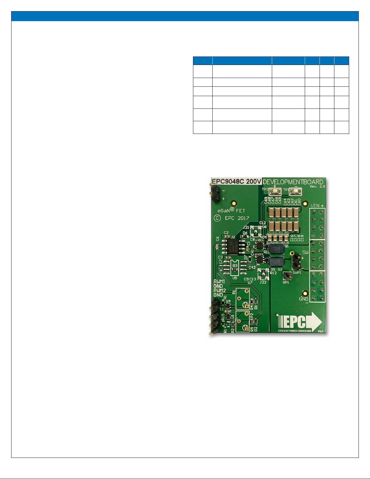
The EPC9048C development board shown in gure 1 is a 200 V maximum
device voltage, 15 A maximum output current, half bridge with onboard
gate drives, featuring two EPC2034C enhancement mode (eGaN®) eld
eect transistors (FETs). The purpose of this development board is to
simplify the evaluation process of the EPC2034C eGaN FETs by including
all the critical components on a single board that can be easily connected
into any existing converter.
The EPC9048C development board is 1.5”x 2”and contains two EPC2034C
eGaN FETs in a half bridge conguration. As supplied, the high side gate
drive uses a digital isolator and both FETs use the Texas Instruments
UCC27611 gate driver. The board also contains all critical components
and layout for optimal switching performance. There are also various
probe points to facilitate simple waveform measurement and eciency
calculation, as well as the option to add trimmer resistors for adjustable
deadtime to provide separate high and low side inputs, and an isolator for
the low side gate drive. A block diagram of the circuit is given in gure 2.
For more information on the EPC2034C please refer to the datasheet
available from EPC at www.epc-co.com. The datasheet should be read in
conjunction with this quick start guide.
QUICK START PROCEDURE
Development board EPC9048C is easy to set up to evaluate the
performance of EPC2034C eGaN FETs. Refer to gure 3 for proper connect
and measurement setup and follow the procedure below:
1. With power o, connect the input power supply bus to +VIN (J5, J6) and
ground / return to –VIN (J7, J8).
2. With power o, connect the switch node (SW) of the half bridge OUT
(J3, J4) to your circuit as required (half bridge conguration).
3. With power o, connect the gate drive power supply to +VDD
(J1, Pin-1) and ground return to –VDD (J1, Pin-2).
4. With power o, connect the input PWM control signal to PWM
(J2, Pin-1) and ground return to any of the remaining J2 ground pins
(J2 Pin-2 or J2 Pin-4).
5. Turn on the gate drive supply – make sure the supply is between 7.5 V
and 12 V range.
6. Turn on the controller / PWM input source.
7. Turn on the bus voltage to the required value (do not exceed the
absolute maximum voltage) and probe switching node to see
switching operation.
8. Once operational, adjust the PWM control, bus voltage, and load within
the operating range and observe the output switching behavior,
eciency and other parameters.
9. For shutdown, please follow steps in reverse.
NOTE. When measuring the high frequency content switch node, care must be taken
to provide an accurate high speed measurement. An optional two pin header (SWP1) is
included for switch node measurement. It is recommended to install measurement point on
backside of board to prevent contamination of the top side components.
For information about measurement techniques, please review the how to GaN series:
HTG09- Measurement
http://epc-co.com/epc/DesignSupport/TrainingVideos/HowtoGaN/
Figure 1: EPC9048C development board
Table 1: Performance Summary (TA= 25°C) EPC9048C
Symbol Parameter Conditions Min Max Units
VDD Gate Drive Input Supply Range 7.5 12 V
VIN Bus Input Voltage Range(1) 160 V
IOUT Switch Node Output Current (2) 15 A
VPWM
PWM Logic Input Voltage
Threshold
Input ‘High’
Input ‘Low’
3.5
0
6
1.5
V
V
Minimum ‘High’ State
Input Pulse Width
VPWM rise and
fall time < 10ns 100 ns
Minimum ‘Low’ State Input
Pulse Width (3)
VPWM rise and
fall time < 10ns 100 ns
(1) Maximum input voltage depends on inductive loading, maximum switch node ringing must be kept under
200 V for EPC2034C.
(2) Maximum current depends on die temperature – actual maximum current with be subject to switching
frequency, bus voltage and thermal cooling may be lower or higher. Please see the EPC2034C datasheet for
further information.
(3) Limited by time needed to ‘refresh’ high side bootstrap supply voltage.

QUICK START GUIDE EPC9048C
EPC – THE LEADER IN GaN TECHNOLOGY | WWW.EPC-CO.COM | COPYRIGHT 2019 | | 3
Figure 3: Proper connection and measurement setup.
Figure 4: Typical Waveform forVIN = 150 V to 12VOUT, 15 A, ~180 W, ~300 LFM airow, 100 kHz buck converter
Figure 2: Block diagram of EPC9048C development board.
VGSL
VSW
IL
VDD
Q1
D
BTST
Q2
PWM
GND
Gate drive
regulator
Digital
Isolator
Logic and
dead-time
adjust
VIN
VSW
CBypass
PGND
Digital
Isolator
Gate driver
with LDO
Gate driver
with LDO
VDD supply
(note polarity)
7.5 – 12 V
Half bridge conguration
Switch node
(For eciency
measurement)
+
+
–
VVA
IN
IIN
+
+
–
–
PWM input
Optional MMCX
jacks for gate drive
measurement
External circuit
Optional 2-pin header for switch node measurement
VIN
supply
+
+

QUICK START GUIDE EPC9048C
EPC – THE LEADER IN GaN TECHNOLOGY | WWW.EPC-CO.COM | COPYRIGHT 2019 | | 4
THERMAL CONSIDERATIONS
The EPC9048C development board showcases the EPC2034C eGaN FET.
The EPC9048C is intended for bench evaluation with typical room ambient
temperature. The addition of heat-sinking and forced air cooling can
signicantly increase the current capability of these devices, but care must
be taken to not exceed the absolute maximum die temperature of 150° C.
NOTE. The EPC9048C development board does not have any current or thermal
protection on board.
For more information regarding the thermal performance of EPC eGaN FETs, please
consult:
D. Reusch and J. Glaser, DC-DC Converter Handbook, a supplement to GaN Transistors for
Ecient Power Conversion, First Edition, Power Conversion Publications, 2015.
Table 2: Bill of Materials
Item Qty Reference Part Description Manufacturer Part #
1 5 C1, C2, C3, C10, C11
Capacitor, 1 μF, 10%, 25 V, X5R Murata
GRM188R61E105KA12D
2 1 C6
Capacitor, 100 pF, 5%, 50 V TDK
C1608C0G1H101J080AA
3 4 C8, C9, C12, C13
Capacitor, 0.22 μF, 10%, 16 V, X7R TDK
C1005X7R1C224K050BC
4 4 C16, C17, C18, C19
Capacitor, 0.1 μF, 10%, 250 V, X7T TDK
C2012X7T2E104K125AE
5 1 C41
Capacitor, 10 pF, 5%, 50 V Kemet
C0402C100J5GACTU
6 1 C42
Capacitor, 100 pF, 5%, 50 V TDK
C1005C0G1H101J050BA
7 10 "C60, C61, C62, C63,C64,C65,
C66, C67, C68, C69"
Capacitor, 0.22 μF, 10%, 250 V, X7T TDK
C3216X7T2E224K160AA
8 2 D1, D2
Schottky Diode, 30 V, 30 mA Diodes Inc.
SDM03U40-7
9 1 D3
Schottky Diode, 200 V, 1 A Diodes Inc.
DFLS1200
10 2 R12, R14
Resistor, 4.7 Ω, 1%, 1/16 W Stackpole
RMCF0402FT4R70
11 2 D6, D7
Zener Diode, 5.61 V, 500 mW On Semiconductor
MM5Z5V6ST1G
12 1 GP1
Connector, .1" Male Vert. Würth
61300111121
13 2 J1, SWP1
Connector, .1" Male Vert. Würth
61300211121
14 1 J2
Connector, .1" Male Vert. Tyco
4 pins of 4-103185-0-04
15 1 "J3, J4, J5,
J6, J7, J8"
Connector, .1" Male Vert. FCI
4 pins of 68602-224HLF
16 2 Q1, Q2
eGaN® FET, 200 V, 8 mΩ EPC
EPC2034C
17 1 R1
Resistor, 10.0 kΩ, 1%, 1/10 W Stackpole
RMCF0603FT10K0
18 2 R2, R3
Resistor, 0 Ω, 1/10 W Panasonic
ERJ-3GEY0R00V
19 1 R4
Resistor, 100 Ω, 1%, 1/10 W Stackpole
RMCF0603FT100R
20 1 R5
Resistor, 470 Ω, 1%, 1/10 W Stackpole RMCF0603FT470R
21 1 R6
Resistor, 0 Ω, 1/10 W Panasonic ERJ-2GE0R00X
22 2 R11, R12
Resistor, 1 Ω, 1%, 1/16 W Stackpole RMCF0402FT1R00
23 2 TP1, TP2
Test Point Keystone 5015
24 1 U1
IC, Logic Fairchild NC7SZ00L6X
25 1 U2
IC, Opto-coupler Silicon Labs
Si8610BC
26 1 U4
IC, Logic Fairchild
NC7SZ08L6X
27 2 U6, U7
IC, Gate driver TI
UCC27611
Table 2: Bill of Materials
Item Qty Reference Part Description
1 DNP P1, P2 Optional potentiometer
2 DNP R21, R22 Optional resistor
3 DNP U5 Optional IC

QUICK START GUIDE EPC9048C
EPC – THE LEADER IN GaN TECHNOLOGY | WWW.EPC-CO.COM | COPYRIGHT 2019 | | 5
Figure 5: EPC9048C - Schematic
1
2
5
1
2
5
0 Ω
0.22μF
V
12
0.22 μF,
1
2
3
4
1
2
1
10
1
255
0 Ω
15
Ω
V
100 Ω
100 V
1
2 5
12 V
1 μF, 25 V
10
1 μF,
25 V
11 1 μF,
25 V
1 μF,
25
ClassName: HighVoltage Gate
Net Class
V
25
1
25
1
0.22 μF,
V
0.22 μF,
V
1μF,
25 V
0.1 μF,
250 V
0.1 μF,
250 V
0.1 μF,
250 V
12 1 Ω
11 1 Ω
Local Fiducials
1
Ground Post
0.22 μF,
250 V
0.22 μF,
250 V
0.22 μF,
250 V
0.22 μF,
250 V
0.22 μF,
250 V
0.22 μF,
250 V
0.22 μF,
250 V
0.22 μF,
250 V
0.22 μF,
250 V
0.22 μF,
250 V
10 V
100
0 Ω
V
1
2
3
4
1
2
1
2
Switch Node SIP Probe
V
21 22
2 21 1
0 Ω
2 22 1
MMCX Gate Probes
V
0.1 μF,
250 V
1 2
5V
5V
200 V, 1
30 V, 30 mA
1
2
3
4
4
3
2
1
4
3
2
1
0 Ω
1
2
3
4
4
3
2
1
16 V

EPC Products are distributed through Digi-Key.
www.digikey.com
Demonstration Board Notication
The EPC9048C board is intended for product evaluation purposes only. It is not intended for commercial use nor is it FCC approved for resale. Replace components on
the Evaluation Board only with those parts shown on the parts list (or Bill of Materials) in the Quick Start Guide. Contact an authorized EPC representative with any questions.This board is
intended to be used by certied professionals, in a lab environment, following proper safety procedures. Use at your own risk.
As an evaluation tool, this board is not designed for compliance with the European Union directive on electromagnetic compatibility or any other such directives or regulations. As board
buildsareat times subjecttoproduct availability, it ispossible that boardsmay containcomponentsor assembly materials thatarenot RoHS compliant.Ecient PowerConversionCorpora-
tion (EPC) makes no guarantee that the purchased board is 100% RoHS compliant.
The Evaluation board (or kit) is for demonstration purposes only and neither the Board nor this Quick Start Guide constitute a sales contract or create any kind of warranty, whether express
or implied, as to the applications or products involved.
Disclaimer: EPC reserves theright at any time,without notice,to makechanges to any products described herein to improve reliability, function, or design. EPCdoes not assume any liability
arising out of the application or use of any product or circuit described herein; neither does it convey any license under its patent rights, or other intellectual property whatsoever, nor the
rights of others.
For More Information:
or your local sales representative
Visit our website:
www.epc-co.com
Sign-up to receive
EPC updates at
bit.ly/EPCupdates
or text“EPC”to 22828
Table of contents
Other IEPC Motherboard manuals


