User Guide 023
UG023.1
May 28, 2015
2
Submit Document Feedback
Functional Description
The ISL9120IIx-EVZ evaluation boards provide simple platforms
to demonstrate the feature of the ISL9120 buck-boost regulator.
The ISL9120IIN-EVZ is for the fixed 3.3V output IC ISL9120IINZ.
The ISL9120IIA-EVZ is for the adjustable output IC ISL9120IIAZ.
The evaluation boards have been functionally optimized for best
performance of the ISL9120 IC series. The input power and load
connections are provided through multipin connectors for high
current operations.
The ISL9120IIA-EVZ evaluation board schematic is shown in
Figure 5, on page 3. The board’s enable function is controlled by
the on-board jumper header J3. Similarly, the forced bypass
function is controlled by the on-board jumper header J4. The
schematic for the ISL9120IIN-EVZ is shown in Figure 7. The PCB
layout images for all layers are shown in Figures 8 and 9. The bill
of materials for the ISL9120IIA-EVZ are shown in Table 2 on
page 4. The bill of materials for the ISL9120IIN-EVZ are shown in
Table 3 on page 5.
Operating Range
The VIN range of the boards is 1.8V to 5.5V. The VOUT range for the
ISL9120IIA-EVZ is 2V to 5V. The IOUT range of the boards is 0 to 1A.
The operating ambient temperature range is -40°C to +85°C.
Quick Start Guide
For the ISL9120IIA-EVZ board, the default output voltage is set at
3.3V. Should other output voltages are desired, resistor R2can
be changed to set to a desired voltage as shown in Table 1 (use a
resistor with 1% accuracy).
Refer to the following Quick Setup Guide to configure and power
up the board for proper operation. During the power-on process,
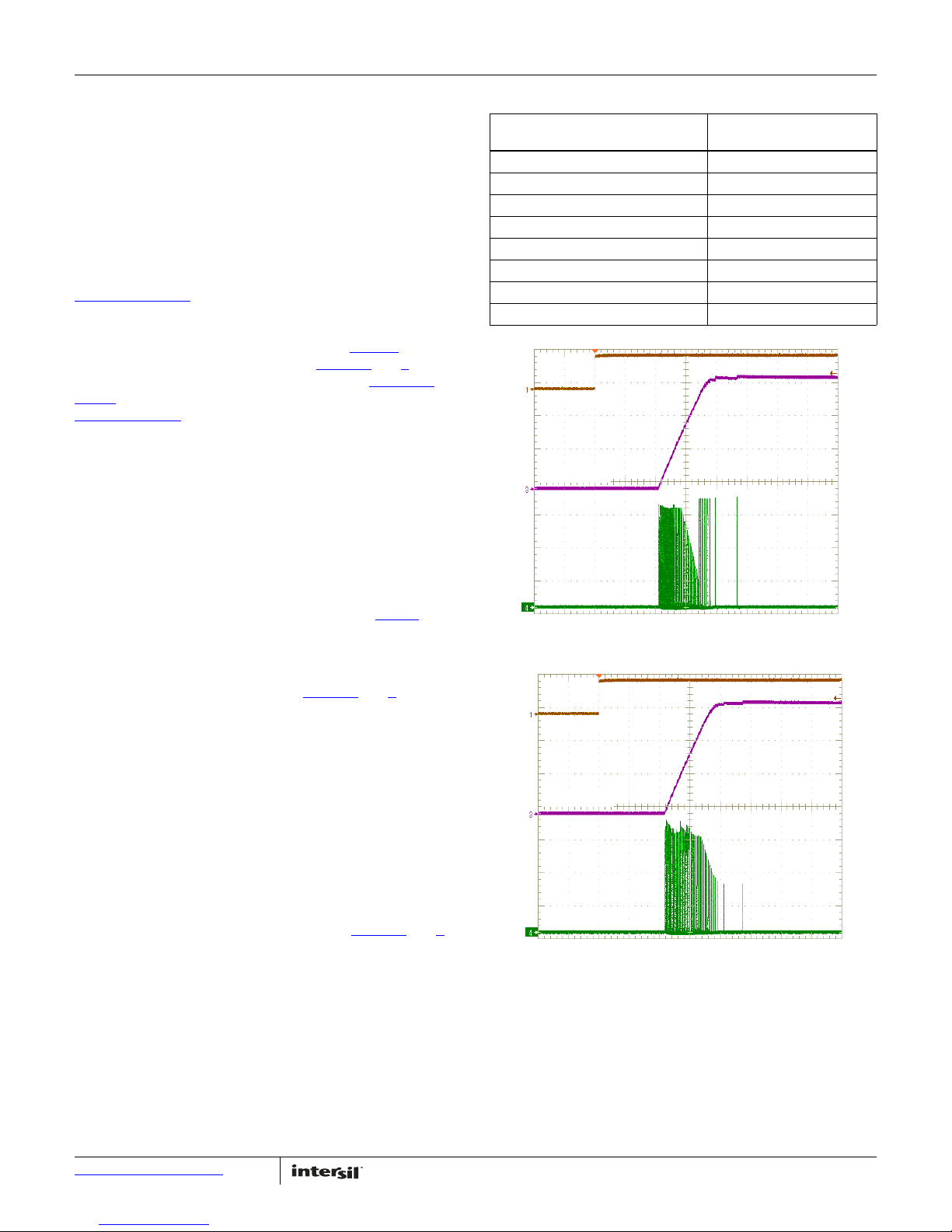
the expected waveforms are shown in Figures 2 and 3.
Quick Setup Guide
1. Install jumper on J3, shorting EN to VIN.
2. Install jumper on J4, shorting BYP to GND.
3. Connect power supply to J1, with voltage setting between
1.8V and 5.5V.
4. Connect electronic load to J2.
5. Place scope probes on the VOUT test point and other test
points of interest.
6. Turn on the power supply.
7. Monitor the output voltage start-up sequence on the scope. The
waveforms will look similar to that shown in Figures 2 and 3.
8. Turn on the electronic load.
9. Measure the output voltage with the voltmeter. The voltage
should regulate within datasheet spec limits.
Recommended PCB Layout
Correct PCB layout is critical for proper operation of the ISL9120.
The input and output capacitors should be positioned as closely
to the IC as possible. The ground connections of the input and
output capacitors should be kept as short as possible and should
be on the component layer to avoid problems that are caused by
high switching currents flowing through PCB vias.
TABLE 1. OUTPUT VOLTAGE PROGRAMMING For ISL9120IIA-EVZ
DESIRED OUTPUT VOLTAGE
(V)
R2RESISTOR VALUE
(k)
2.0 124
2.5 88.7
3.0 68.1
3.3 60.4
3.4 57.6
4.0 46.4
4.5 40.2
5.0 35.7
FIGURE 2. SOFT-START (VIN = 3V, VOUT = 3.3V, NO LOAD)
FIGURE 3. SOFT-START (VIN = 4V, VOUT = 3.3V, NO LOAD)
EN (2V/DIV)
VOUT (1V/DIV)
IL (500mA/DIV)
400µs/DIV
400µs/DIV
EN (2V/DIV)
VOUT (1V/DIV)
IL (500mA/DIV)


