UG122 Rev.0.00 Page 4 of 15
Sep 18, 2017
ISL70321SEHEVxZ 2. Functional Description
2. Functional Description
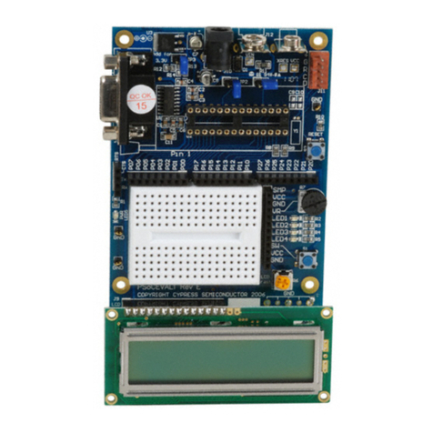
The ISL70321SEHEV1Z evaluation board provides a simple platform to demonstrate the functionality and features of
the ISL70321SEH sequencer IC. The default configuration is a standalone mode wherein the ENx outputs are fed back
to the VMx inputs so that the sequencing operation can be demonstrated. Using a combination of jumper settings, the
ISL70321SEHEV1Z can be used to address the enable inputs of multiple Intersil POL or LDO evaluation boards using
the ENx outputs to create a sequenced on and off multi-voltage rail power supply block.
A common delay timing between the sequenced ENx outputs can be adjusted by changing the TDLY resistor values.
Likewise, the power-good timer can be adjusted so that various ramp times of the enabled power supplies can be
predetermined.
2.1 Operating Range
By default, the ISL70321SEHEV1Z is configured for the operating VIN range of 3V to 13.2V. The ENx, DONE,
and KILL outputs are pulled up resistively to the VCC5 output. These outputs can be pulled to another voltage once
jumpers are removed. The sequence delay and power-good timers are set to 2ms and 4ms, respectively.
2.2 Quick Start Guide
2.2.1 Single IC Stand-Alone Operation (ISL70321SEHEV1Z)
(1) Ensure that the board is properly connected to the supply and loads prior to applying any power.
(2) Connect the input supply to VIN and GND.
(3) Signal UP high, monitor the four ENABLE outputs with an oscilloscope to see them go high in order.
(4) Signal UP low, monitor the four ENABLE outputs with an oscilloscope to see them go low in reverse order.
2.2.2 Dual IC Cascaded Stand-Alone Operation (ISL70321SEHEV2Z)
(1) Ensure that the board is properly connected to the supply and loads prior to applying any power.
(2) Connect the input supply to VIN and GND.
(3) Signal UP high, monitor the eight ENABLE outputs with oscilloscopes to see them go high in order.
(4) Signal UP low, monitor the eight ENABLE outputs with oscilloscopes to see them go low in reverse order.
2.2.3 Sequence Power Supplies
(1) Change the delay and power-good timer resistors on the board as necessary to achieve the desired timing of
sequenced events through the provided resistor positions. Take into account the rise times of the power
supplies and the VM input threshold voltage.
(2) Connect the appropriate bias supply to VDD and GND.
(3) Connect the enabling input of the POL or LDO power supplies to be sequenced to the appropriate
ISL70321SEH ENx outputs in the order of desired turn-on sequence.
(4) Connect the power supply outputs to the appropriate ISL70321SEH VMx inputs.
(5) Connect UP to the appropriate signaling input.
(6) Use oscilloscopes and DVMs to monitor signals and voltages.
(7) Turn system input power supply ON.
(8) Signal the UP input.
(9) Observe sequencing function and adjust timing and threshold voltages as desired.
