TABLE OF CONTENTS
F32700N25.doc Page 2
SECTION 1: THEORY OF OPERATION.....................................................................3
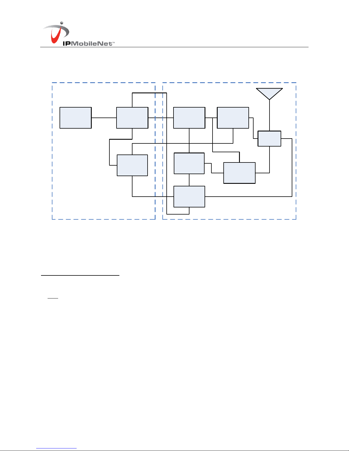
General Block Diagram....................................................................................3
General Block Diagram Definitions..........................................................3
F32700N25 Fixed Radio Section Descriptions...............................................5
Microcontroller.........................................................................................5
Support Circuitry..........................................................................5
Inputs/Outputs .........................................................................................5
Modem.....................................................................................................6
VLogic and Digital Ground.......................................................................6
Receiver 1 Front-End...............................................................................7
Receiver 1 IF ...........................................................................................7
Transmit Modulation ................................................................................7
Injection Synthesizer................................................................................8
Transmitter/TR Switch .............................................................................8
Power and Analog Ground.......................................................................8
SECTION 2: FACTORY TEST PROCEDURE.............................................................9
Equipment List..................................................................................................9
Programming and Configuring Fixed Radio ................................................10
Adjustment / Alignment Procedures.............................................................11
Receiver Injection ..................................................................................11
Receiver.................................................................................................11
Transmit Data........................................................................................12
Transmit Power Control.........................................................................12
Receive Data.........................................................................................13
Final Test...............................................................................................13
Uplink Hardware Timing Verification......................................................15
Downlink Hardware Timing Verification .................................................17
SECTION 3: FCC LABEL..........................................................................................19
F32700N25 Data Transceiver FCC Label Placement ...................................19
F32700N25 Data Transceiver FCC Label ......................................................19
APPENDIX A: F32700N25 CIRCUIT BOARD DIAGRAMS ......................................20
APPENDIX B: F32700N25 TEST DATA SHEET ......................................................21