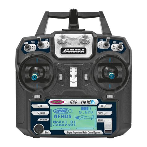
JR NET-ZS75 User manual

Page 1
Technical Report
Transmitter Module Model NET-ZS75
FCC ID# BRWNETZS75
T A B L E O F C O N T E N T S
1.0 INTRODUCTION
1.1 Definition
1.2 Application
1.3 Construction
2.0 ENCODER THEORY OF OPERATION
3.0 THEORY OF OPERATION
3.1 General
3.2 Block Diagram
4.0 FAILURE ANALYSIS
5.0 APPENDICES
5.1 Transmitter Block Diagram
5.2 Transmitter Schematic Diagram
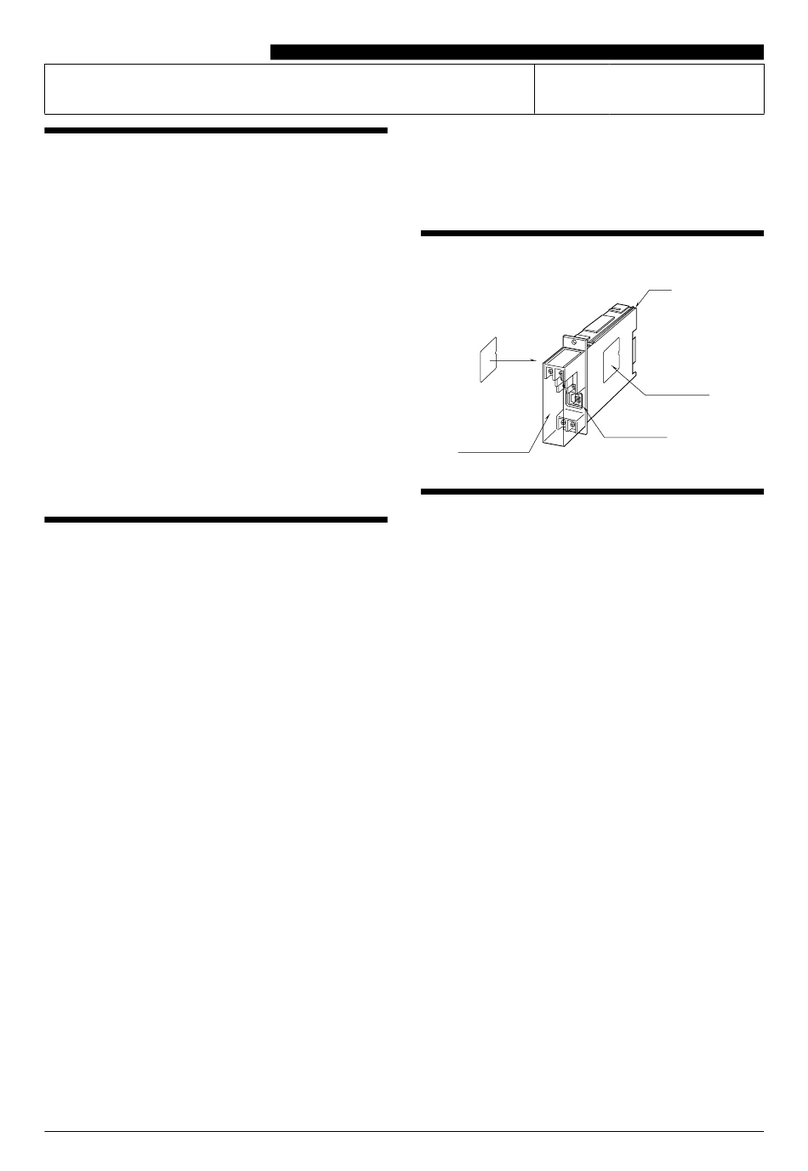
5.3 Transmitter Photographs and ID Labels
5.4 Transmitter Tune-Up Procedure
5.5 Quarts Crystal Specifications
5.6 Test Data

Page 2
Technical Report
Transmitter Module Model NET-ZS75
FCC ID# BRWNETZS75
1.0 INTRODUCTION
1.1 Definition
The Model NET-ZS75 is a transmitter Module for the Remote
Control(R/C) of models such as cars, boats,etc.
and NET-ZS75 is used by plugging into the Transmitter(main body
for control).
This Transmitter module is for FM PLL System, available for the
PPM(Pulse Position Modulation).
The latest type of Model Z-1 will be utilized for the application
of this Transmitter module NET-ZS75.
This Transmitter module is a part of the HORIZON HOBBY DISTRIBUTORS,
INC. PPM "family" of Remote Control Transmitters which at this
time consists of:
Transmitter Model # FCC ID #
NET-J75P BRW8ZCNET72FP
XS3 BRWXS3
XR-3 BRWXR-3
Separate Applications for each transmitters and for the receivers
are submitted as required by the Commission.
The Manufacturer, Japan Remote Control Company (JR),manufactures
all transmitters and receivers.
The PPM family of R/C systems is exported by JR to the United States
of America, and several European and Asian Countries.
The Applicant for this Equipment Authorization, HORIZON HOBBY
DISTRIBUTORS,INC. will, following receipt of Grant of Equipment
Authorization, import only those versions of these R/C radios
which are allowed for use in the USA under the Rules and Regulations
of the Federal Communications.
The 75 - 76 MHz version of this transmitter is the subject of this
Application; these are the units which will be offered for sale
to the general public.

Page 3
Technical Report
Transmitter Module Model NET-ZS75
FCC ID# BRWNETZS75
1.2 Application
The Model NET-ZS75 R/C transmitter module utilizes
" Phase Locked Loop " and " Frequency Modulation " to convey the
PPM encoded position handle and trigger switches to its companion
R/C receiver, where the PPM encoded pulse train is demodulated,
decoded, and supplied to a number of servo-mechanisms for
positioning of control surfaces, throttle etc. on the model.
The Frequency-Shift-Keying of the transmitter carrier takes place
in the rhythm of the PPM pulse train.
Both transmitter and receiver are very narrow band units; they
have been designed to comply with the European requirements of
10 KHz channel spacing.
1.3 Construction
The Model NET-ZS75 Transmitter module all consists of a plastic
case.
(Reference is made to Fig. 5.1, Transmitter Block Diagram)
* control handle and trigger and switches
* a 8sells dry battery
* an analog-to-digital converter (ADC)
* a microprocessor to create the PPM pulse train
* a modulator driver stage
* a RF power stage
* a telescopic antenna
This Transmitter module is to be made available by the importer
only on those carrier frequencies in the 75 - 76 MHz frequency
band which are at present authorized for R/C use.

Page 4
Technical Report
Transmitter Module Model NET-ZS75
FCC ID# BRWNETZS75
2.0 ENCODER THEORY OF OPERATION
Reference is made to Figure 5.1, Transmitter Block Diagram.
The functions of the encoder are to:
* accept the analog voltages from the control inputs.
(handle and trigger.)
* process the analog voltages to create control mixing, adding,
reversing, etc., as desired by the user.
* sample these voltages in a cyclic rhythm under control of the
system's internal timing generator.
(This process is called commutation.)
* process these analog voltages into binary weighted digital
control words by means of an Analog-to-Digital Converter
(ADC).
* store these digital representations of the analog control
input into a temporary memory (RAM).
* supply this serial data stream to a buffer-driver for
modulation of the RF Transmitter.
* provide "housekeeping" of the encoding process by means of a
quarts crystal controlled internal clock.
* provide supply voltages to the RF section (Vcc = 12V battery
voltage; Vreg = 5.0V regulated voltage).
The entire program which controls the timing housekeeping,
parallel-to-serial conversion process, and insertion of
Synchronization words and error detection codes is governed
by a Central Processing Unit (CPU) under control by an
internally stored program residing in Read-Only Memory (ROM).
The CPU, RAM and ROM are all part of a single-chip microprocessor.
Resolution of the Analog-to-Digital conversion process is ten
(10) bits for a control accuracy of 1:210 .

Page 5
Technical Report
Transmitter Module Model NET-ZS75
FCC ID# BRWNETZS75
3.0 THEORY OF OPERATION
3.1 General
The RF Transmitter itself is located in a plug-in,
hermetically sealed, module.
It operates on any of the R/C frequency (Channels)
allowed by the Commission in the 75 – 76 MHz frequency band.
Selection of the desired RF channel is made by PLL frequency data.
This transmitter employs Frequency-Sift-Keying (FSK)of the carrier
frequency, whereby the output frequency is either
low or high due to the symmetrical FSK modulation process, the
(center)output frequency cannot be directly measured, but must be
calculated by taking the average of the high and low frequency
states.
The peak-to-peak deviation of the FSK signal is approximately 3.6
KHz ("sliver modulation")
Because of the unfamiliarity of the general public with the
term FSK, this modulation technique is commonly named FM.
mm
flow fhighfC
m= shift from center frequency
( m = approx. 1.8KHz )
2
flow + fhi
g
h
f center =

Page 6
Technical Report
Transmitter Module Model NET-ZS75
FCC ID# BRWNETZS75
3.2 Block Diagram
(Reference is made to Figure 5.1)
The (up to) four control potentiometers are at the upper right
side of the schematic drawing.
The control potentiometer, which is mechanically coupled to the
control handle and trigger,is supplied with the regulated 5.0V
voltage.
The wiper on this pot is exactly centered in the neutral control
handle and trigger position. All analog processing is performed
as deviations from this center (reference) voltage.
After the mixing of each channel, control voltage is changed to
Pulse Train, through encoder circuit.
The Q11(2SC4519)is an LC-type VCO(Voltage Controlled Oscillator),
which is designed to oscillate with about 75.650MHz. Its output is
led to amplifying stage for transmitting through a buffer(Q12),while
it is also led to the PLL through a buffer(Q13). The pulses generated
by the CPU are transferred to the VCO so as to modulate the radio
wave. this part is strictly shielded from electric/magnetic noise.
The IC3(BU2630F)is a PLL(phase Lock Loop).
Exact 13.000MHz is generated by an internal crystal oscillator, and
divided by 5,200 for 2.5kHz.
VCO wave is also divided by a definite number, which is 30,260
in case of 75.650MHz,for getting 2.5kHz.
Two 2.5kHz’s are compared in the phase and the VCO is so controlled
that the error gets minimum, while the modulation is so fast that
the filter between the PLL and the VCO cancels an error fluctuation.
Frequency data is stored in the IC1(MC68HC908QY1/CPU) as an
above-mentioned dividing number, and transferred to the PLL as the
serial data while the transmitter is in normal operation mode.
Frequency data can be changed only in system set-up mode with the
power of the RF section being cut.
Directly after it has turned on normally, though the CPU starts
sending the PLL the data. Then, supply the power to Q1 via Q8(2SC4738)
and Q7(2SA1298) to start oscillation.
Page 7
Technical Report
Transmitter Module Model NET-ZS75
FCC ID# BRWNETZS75
the radio wave is still silent because the RF amplifier (Q1,Q2)is
not supplied with the power yet. After a while, certain stabilizing
time for the PLL, the Q6(2SC4738) and Q4(2SA1298)starts to supply them
with the power so that the radio wave is transmitted.
Q2 drives the Power Amplifier (PA). The straight-through PA stage(Q3)
is followed by a matching and band pass/low-pass network.
This network matches the low PA stage output impedance to the whip
antenna.
DC Supply Voltage enter the RF section: 12 Volt "law" battery voltage
supplies the PA stage only. PLL stages, and bias current for all
stages, including the PA, are derived from the regulated 5.0 Volt.
4.0 FAILURE ANALYSIS
A failure analysis was conducted to ascertain that single-component
failure will not result in unauthorized radiation.
It should be noted that component failure would result in return
of the unit to the factory, or to an authorized repair station.
(Reference is made to Figure 5.2, Transmitter Schematic Diagram)
Failure of any of the transistors (predominant failure mode:
emitter-collector short) will result in the unit becoming
inoperative: In the case of Q11 oscillator short, RF output will
be non-existent.
Q12,Q1,Q2 or Q3 failure will result in very low, if any, output.
Failure of the MOD IN input (latch at 0 or 12 Volt)or modulator
transistor Q9, Q10 and variable diode D4 (open or short) will result
in carrier frequency.
Although this failure would render the unit inoperative, the
frequency tolerance would still fall within the channel bandwidth
and tolerance requirements of .002% of 75 MHz = 1.50 KHz.
When PLL circuit is broken, for example, crystal X1 break down, or
IC101(BU2630) for PLL is broken, PLL will stop functioning.

Page 8
Technical Report
Transmitter Module Model NET-ZS75
FCC ID# BRWNETZS75
5.4 Transmitter R.F. Tune-Up Procedure
1. Remove 2 screws from transmitter Module. Remove PC assembly.
Put PC assembly on bench, component side up.
2. Refer to transmitter schematic Figure 5.2.2.
Soften bee’s wax on cores in L1, L2, L3, L4 ,L5 and L6.
Using oscilloscope with small 50 ohm loop, starting at L1,
adjust these cores for maximum oscilloscope reading.
Repeat this tuning sequence until no further increase in
oscilloscope reading can be obtained.
3. Extend the aerial, and adjust L1, L2, L4, L5, L6
(in this order) to get maximum output. Try 2 times.
4. Shorten the aerial, and adjust L4 to make the current minimum.
5. Extend the aerial fully, and adjust L5 and L6 to get peak.
6. Adjust the frequency.
First, set up the Spectrum Analyzer.
Level Scale is : Log = 5dB/Div, Center Frequency = 75.650Mhz,
Span = 5KHz, RBW = 1KHz, VBW = 1KHz.
Then adjust the Amplitude and Attenuator to the right level.
Then, transmit the frequency Band 75 (75.650Mhz) from the Standard
Transmitter. Then store wave form to the Spectrum Analyzer.
By using VC2 and P2 and p1 in the transmitter, adjust it to make
the same wave form.
7. Confirm the power.
8. Using spectrum analyzer with small 50 ohm loop, verify that
sub harmonic and harmonic components are at least 50dB below
carrier component. Pay special attention to 144MHz components.
9. Remove PCB assembly from Transmitter. Reapply bee’s wax to L1,
L2, L4 , L5 and L6. Put PCB assembly back into its case, replace
the 2 screws.

U1 MPU
VR1:Steering Wheel
VR2: Throttle Triger
SW1
SW2
SW3
SW4
SW5
SW6
SW7
SW8
SW9
SW10
SW11
SW12
SW13
SW14
SW15
SW16
SW17
Voltage Reg(5V)
Key SW
GD PCB
Trim PCB
VDD
Power Supply
DC 9.6-12.0V
Dry Battery or Ni-cd battery Pack
BUZZER
Phone Terminal
Power Indicator
TH:ABS Indicator
TH:Speed Indicator
TH:ACC Indicator
LCD Panel
LCD Back Light
Buf
Buf
Sig Out
to RF Module
DSC Output
Clock Crystal
(RF-501F)
Charger Terminal
FCC ID# BRWNETZS75 Figure 5.1.1 Transmitter Block Diagram
Page 9

Xt al
ANT
mp.
Band Pass
Filt er
Modulator Regulator
VCO
APower Amp
mp.
A
Controller
IC1;
MC68 HC908 QY1
Fr equenc y Sel ect or
SW1,SW2
Power ON/ OFF S W
Q4, Q7 ;2SA1298
Q6, Q8 ; 2SC4738
ANT
GND
Vcc
MOD.
GND
FCC ID# BRWNETZS75 Figure 5.1.2 Transmitter Block Diagram
Transmitter Module NET-ZS75
Page 10

73R 2
0
1
1ZB
512-AP31BC
9
2R
3
7
4
52C
2
0
1
IV
G
OV
4U
F50L87
84R
M
1
43R
374
12C
2
0
143C
201
64R
301
3
3R
3
74
+3C
V52574
22R
37
4
12R
37
4
9C
p
2
2
2C
301
8
2C
201
52R
3
7
4
72R
37
4
6R 222
+
3
1C
V01
u
0
0
1
9
2C
201
5
4
R
k
0
1
33C
201
P95
1
P94
2
P93
3
P92
4
P90
5
CNVss
6
P87
7
P86
8
Reset
9
Xout
10
Vss
11
Xin
12
Vcc
13
P85
14
P84
15
P83
16
INT0
17
P81
18
TA4out
19
P77
20
tuo3AT 1
2
1
7P 2
2
t
u
o
0AT 3
2
76P 42
66P 52
56P 6
2
46
P72
0DX
T8
2
0D
XR 92
1
6
P0
3
0
6P 13
7
5P 23
6
5P 3
3
55P 4
3
4
5P 53
3
5P 63
25P 7
3
15P 83
0
5
P93
3
4P 04
P42 41
P41 42
P40 43
P37 44
P36 45
P35 46
P34 47
P33 48
P32 49
P31 50
P30 51
P27 52
P26 53
P25 54
P24 55
P23 56
P22 57
P21 58
P20 59
P07 60
60P
16
50P
2
6
40
P
36
30P
4
6
2
0P
56
1
0P
66
00P
7
6
7
0
1
P
8
6
6
0
1
P
96
5
0
1
P
07
401P
1
7
3
0
1
P
27
2
N
A
3
7
1NA
47
ssVA
5
7
0
N
A
67
fe
rV
77
cc
V
A
8
7
79
P
9
7
69
P
0
8
1U
A
M
3
2
6
0
3
M
53R
3
7
4
4C
1
0
1
7R
2
7
4
8Q
6
1
1
4
C
S
2
71R
374
11R
372
+2
1C
V01u001
6
5R
4
0
1
0
2C
2
01
22C
201
2U
NS/T
B
61C
L4
2
2D
T
M
0
1
3-L
M
S
42R
3
7
4
3WS -
IV
G
OV
3U
L
MA
1
5915M
1
3C
2
0
1
11C
301
41C
401
23
R
374
8
1R
374
21R
G
3
0
1
5C
1
01
73C
201
4
D
R
V
2
3
3-R
L
S
1W
ST
CE
L
E
S
01R
G3
4
2
9
3R 3
6
5
03C
201
8R 2
2
2
72C
2
0
1
8C
p22
42C
201
5R 222
11
2
2
1L
T5223MEL
5
3C
2
0
1
3
2C
201
02R
3
7
4
51C
401
+83C
V
6
1
u
74
1D
TM0
1
3-L
M
S
0
1C
3
01
1C
3
0
1
82
R
3
7
4
13R
374
32R
374
6
2R
374
91R
374
2WS +
83R
2
0
1
74R
301
3D
TM013-LM
S
03R
3
7
4
6
3C
201
04C
201
6
2
C
201
1X
z
H
M
6
1
23C
201
4WS RETNE
CCV
DDV
FERV
CCV
DDV
CCV
DDV
CCV
FERV
CCV
DDV
CC
V
DDV
Dx
T
DxR
DELREWOP 3R
2
7
4
2
*
8
0
6
1
7C
1
0
1
6C
101
DDV
05
R
00
0
1
5R
000
2
5R
0
00
35R
0
0
0
1
4R
K74
24R
K74
3
4
R
K74
4
4R
K
7
4
DDV
6
1
C
201
71C
201
8
1C
20
1
91C
201
5Q
3
031NR
41R
2
2
2
l
o
rt
n
o
C
t
h
g
iL
kca
B
2R 2
2
2
1R
222
4R
2
2
2
1
2
3
4
5
6
7
8
1J
FT-
3
M
S-RZ-B8B
63R
374
7Q 6
1
1
4C
S
2
75R
k0
0
1
5
5R
201
0
4R
K74
sm61/sm11
e
p
yT
G
O
J
kcol
C
M
61/8
t
h
giLkc
a
B
k
c
aPata
D
DEEPSHT
CCAHT
SB
A
94R
374
C
C
V
+
9
3C
V
616
0
1
61R
30
1
pUl
lu
Pd
ee
NT
RO
P
WSHS
U
P
GOJ:48P
1
2
3
4
5
6
7
8
5PJ
FT-
3
M
S-R
Z-B8
B
1
2
3
4
5
6
6PJ
FT-3MS-RZ-B6B
1
2
3
3PJ
FT-3MS-RZ-B3B
1
2
3
4PJ
FT-3MS-RZ-B3B
FE
R
V
gn
ir
ee
tS
elttorhT
BCP
M
IRTmorF
BCP
DGmo
rF
eludoMataDrof
langiSFRot
1
2
3
4
5
7PJ
FT-
3
M
S-
RZ-B5B
enohP
CCV
l
an
gi
S
CSDot
DNG
11
22
33
4
455
77
6
6
5WS
0
0
2
002PGR
S
)B(GOJ
)
A
(
GOJ
45R
2
2
2
CCV
1
2
3
4
5
6
7
8
9
01
11
21
31
41
1P
J
QS-B41T
1
2
2P
J
Q
S
-
B2
T
1B 1
E2
2B 3
2C
4
1C
5
1Q
3
0
7
1
N
R
1
B
1
E
2
2
B
32
C4
1C 5
2
Q
307
1
NR
4
Q
3
0
3
1
NR
3
Q
3031N
R
5
1
R
32
8
31R
2
22
14C
4
0
1
2
4C
401
44C
3
0
1
34C
301
54C
322
6
4C
3
2
2
74C
3
0
1
SPL
A
:)p
U
(eno
N
M61:
)
pU
(e
n
oN
elbanE:)
p
U(e
n
oN
elb
a
nE
:
)pU(e
noN
cesm11:DNGoT
DN
Gt
c
ennoC:
5
8P
95R
174
DDV
85R
274
1B
1
E
2
2B
32C 4
1C 5
6Q
3071NR
9
4C
1
0
1
84C
101
9R
enoN DDV
0
5
C
20
1
16
R201
20
106
R
26R
374
36R
374
TROPMOC
ecneS
e
c
n
eS
ADS
LCS
m61/11
DDV
5
6
R
222
䎢
䎢䱌
䎻䎶䏒䏃䏛
FCC ID# BRWNETZS75 Figure 5.2.1-1 Transmitter Schematic Diagram
Page 11
/CKP2%$

1
1
2
2
3
3
4
45
5
6
6
4
J
0
10-10-6041
J
S
H
1
2
3
4
5
1
PJ
5
RE
D
AE
H
1E
AN
N
E
TN
A
CSD
eludoM
F
RoT
2C
201
+GHC
-GHC
1D
40SMC
5
J
060
-
10
-
6
0
4
1
J
S
H
EN
O
H
P
1
2
3
4
5
3
J
5NOC
l
angi
S
FRmorF
e
noh
P
CC
V
l
a
ng
i
SCSDmorF
DNG
1
2
3
4
5
6
7
8
2
J
8
NOC
1
2
3
4
5
6
7
8
1
J
8
NOC
NOMM
O
C
1CN 2
ON 3
1
S
7SSSS
nitacinumoC&kcaPataDoT
BC
P
niaM
m
orF
1
2
3
4
2
PJ
4REDAEH
NO-WS
GHC
WS
REWOPCSD
DNG
6
J
GHC
1
24PJ
REPMUJ
1
2
3
P
J
R
E
P
MU
J
1C
201
2
L
H
u0
01
1L
Hu001
1
2
5
PJ RE
PM
UJ
2D
40SMC
EX-10 RF Mount
12
6
W
S)
-
(
2T
E
12
7WS 2NTB
12
5WS )+
(
2T
E
12
1
WS
)+(3T
E
12
3WS )+
(
1T
E
12
2WS )-(3T
E
12
4WS )
-(1T
E
1
2
3
4
5
6
7
8
1J
8NOC
BCPMRTsuoileH
1
2
3
2PJ
3R
E
DA
E
H
niPredaeHdciNroF
y
r
ettaByrDmorFB
CP
WSoT
1
2
1PJ
2REDAEH
1
2
3P
J
2
RE
D
AE
H
t
c
e
n
noC
y
r
ett
a
Bdc-iN
11
2
2
3
3
44
5
5
6
6
1S
WSREWOP
1
2
3
4
1PJ
4REDAEH
1
2
3P
J
2
RE
DA
EH
n
idciN
N
O-
W
S
G
H
C
WS
R
E
WOP
C
SD
DNG
W
S
r
e
w
oP
s
oil
e
H01-XE
FCC ID# BRWNETZS75 Figure 5.2.1-2 Transmitter Schematic Diagram
Page 12

DA
CK
CE
TO HOST COMPUTER
Z102-A/Z102-B
Z101-A/Z101-B
f0
TP=2.5v
73C
301
R11
8.2
6C
p
1HC
8R
33
7C
3
0
1
5R
k21
C3
CH47p
3R
3
3
1
C
p5HC
2C
301
R1
100
2
3
C
301
L8
HW601
03C
2
0
1
R16
47k
71R
k01
R25
10k
94C
2
0
1
C80
B471
TP
R58
3.3k
09C
301
D1
JPW
88C
5
01B
R55
NON
1
8
C
374B
3
5R
k8.6
25R
74
R51
2.2k
R54
10k
R49
100k
C18
CH30p
C13
NON
61
C
NON
01R
k3.3
C25
CH5p
C22
NON
C19
NON
21C
NON
SW1
X1
2
C
81
C
4
8
9
2
1
0
4
3
7
65
L5
TP-7T
L4
TP-6T
Q3
2SC4910
21R
8.
6
3
1R
8.6
41R
8.6
4
1C
201
02C
P
0
01HC
32
C
p
3
3HC
7R
2
2
6R
k3.3
5C
20
1
Q2
2SC4519-6
Q4
2SA1298Y
1
3C
2
0
1
93C
40
1
4
2R
k01
Q6 2SC4738Y
53C
NON
+
R9
220
92R
k01
R30
10k
C21
CH15p
R26
39k
4C
301
R4
JPW
L1
TS-72S
1
2
3
6
4
L2
TS-72S
1
2
3
4
6
SW2
X10
2
C
81
C
4
0
5
1
2
6
9
8
73
4
ANT
CN1
7B GND
8B Vcc
9B GND
10B MOD
ANT.
C11 CH150p
IC2
78L05F
1
O
2
G
3I
D7
HSC119
65
C
V3
.6
/F
u
0
1
85C
301
R64 10k
65
R
NON
C94
NON
6D
NON
R63 10k
R65 10k
02
R
k01
24C
2
01
R21
10k
R19
10k
Q5
2SC4738Y
Q13
2SK882
R50
1k
C78
CH47p
04R
k74
3D
092VS1
C63
CH7p
11L
Hu22.0
VC1
6pF
1
4R
k01
2
4R
k21
4D
0
9
2VS1
86C
p
2HC
66C
p28
HC
76
C
p86HC
27C
p1HC
C73
CH3p
R46
680
74R
k
6
5
Q12
2SK882
84R
0
65
C74
C
CH22p
0
7C
201
34R
k74
96C
N
ON
C62 UJ4pF
C65
CH12p Q11
2SC4519-6
1
P
k
1
25C
174B
63R
9
3
4
5C
NON
Q9
2SC4738Y
Q10
2SC4738Y
C53
B182J
R37
180
15C
20
1
R31
10k
R33
39k
8
3R
0
2
8
06C
4
0
1
R39
3.3k
55C
274B
26R
k01
R61
47k
C50
102
Q7
2SA1298Y
Q8
2SC4738Y
L15A
10
44
R
0
8
1
54R
3
3
28C
301
72R
k
0
1
04C
NON
14C
sc
i
ma
r
eC
V3.6/Fu01
+
38C
s
c
im
ar
eC V3.6/Fu01
+
74C
mulatn
aT
V
3
.
6
/F
u
0
1
+
17C
mulatnaT
V3.6/Fu01
+
67C
mulatnaT
V
3
.
6/F
u0
1
+
97C
mulatnaT
V3.6/Fu01
+
98C
mulatnaT
V3.6/Fu01
+
44C
NON
2CV
Fp6
X1
13.00MHz
IC3
BU2630F
1XIN
2Vss
3RPD
4P-R
5RON
6F-R
7CE
8CK 9
DA
10
LD
11
F-T
12
TON
13
T-P
14
TPD
15
VDD
16
XOUT
CN3
1
2
3
4
CN2B
1B
2B
3B
4B
5B
6B
C64
CH10p
9
5C
V02/Fu1
CN2
1
2
3
4
5
6
IC1
MC68HC908QY1 TSSOP
1PTA0
2PTB1
3PTB0
4Vss
5VDD
6PTB7
7PTB6
8PTA5 9
PTA4
10
PTB5
11
PTB4
12
PTA3
13
PTA2
14
PTB3
15
PTB2
16
PTA1
OSC1 OSC2
IRQ
RST
R57
100k
5D
B053CVH
5
1C
301
C27
103
51R
0
7
4
7L Hu3.3
CN4
1
D
D
V
Q
RI
zzub/FR.jdAATAD
DNG
M
8
.21N
I
WS.KHC
1A
TP
2
AT
P
2P k74
CN3B
1B
2B
Mod
3B
Duty
4B
95
R
k7.4
5
3R
k22
23R
k
8
.
5
L6
TP-5T
71
C
p
6
5
HC
C87
UJ 56p
68C
p5
JU
58C
p51JU
L9
HW601
A21L
106WH
41L
1
0
6WH
A8L
WPJ
011
C
301
81
R
k
0
1
3
3
C
sci
m
areC
V3
.
6/Fu
0
1
+
43C
301
Q1
2SK882
2
R
k
0
1
FCC ID# BRWNETZS75 Figure 5.2.2 Transmitter Schematic Diagram
Page 13

Page 14
SPECIFICATION OF CRYSTAL UNIT
1.FREQUENCY 13.000000MHz
2.HOLDER TYPE SMD SX-2112
3.FREQUENCY TOLERANCE +- 20 PPM / +25C
4.EQUIVALENT RESISTANCE 30 OHM MAX / SERIES
5.OPERABLE TEMPERATURE RANGE -30C --------- +80C
6.TEMPERATURE DRIFT +- 10 PPM
7.LOADING CAPACITY 10 PF
8.DRIVE LEVEL 20 uW
9.SHUNT CAPACITY 1.8 PF MAX
10.MODE OF OSCILLATION FUNDAMENTAL
11.INSULATION RESISTANCE 500M OHMS MIN AT 100V DC
12.SHOCK TEST
DROPPING FROM 120cm HIGHT 10 TIMES HARD WOODEN BOARD
( Drop it onto a hard wooden board ( Thickness : 30mm ) hor 6 directions ( XX’YY’ZZ’ ),
This should be 1 cycle )
VARIATION : FREQUENCY LESS THAN +-2 PPM
: RESISTANCE LESS THAN 2 OHM or +- 15 % ( wnichever is lager )
13.VIBRATION TEST
FREQUENCY 10 TO 55Hz ; AMPLITUDE 1.5mm P-P 1 MINUTES
TEST TIME : XYZ each direction 2h
VARIATION : FREQUENCY LESS THAN +-2 PPM
: RESISTANCE LESS T THAN 2 OHM or +- 15 % ( wnichever is lager )
14.AGING
+- 1 PPM max / YEAR
Figure 5.5 Crystal Specification

Page 15
FCC ID# BRWNETZS75

Page 16

Page 17
FCC ID# BRWNETZS75

Page 18
FCC ID# BRWNETZS75
Table of contents
Other JR Transmitter manuals