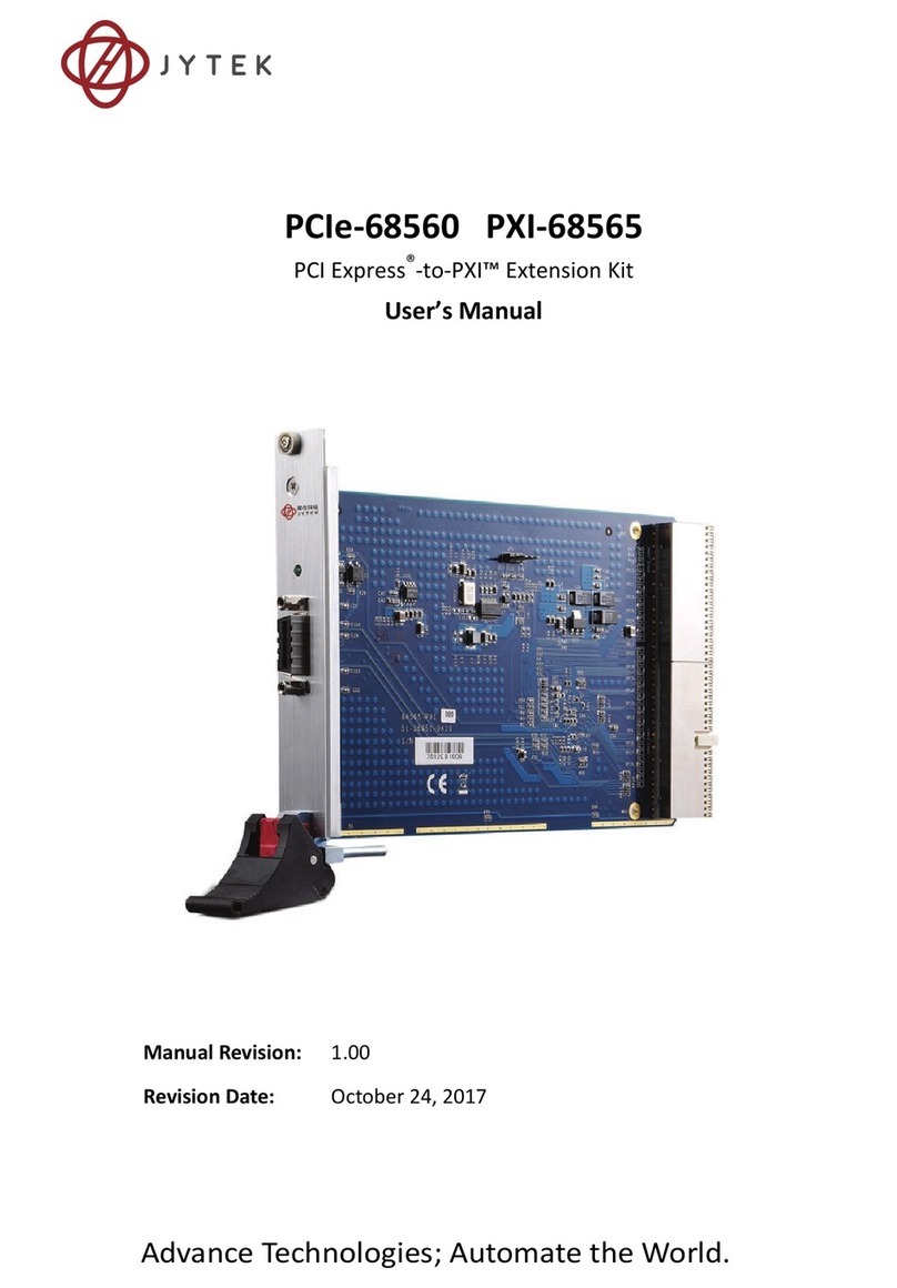
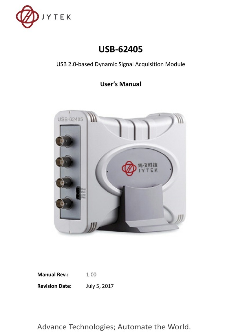
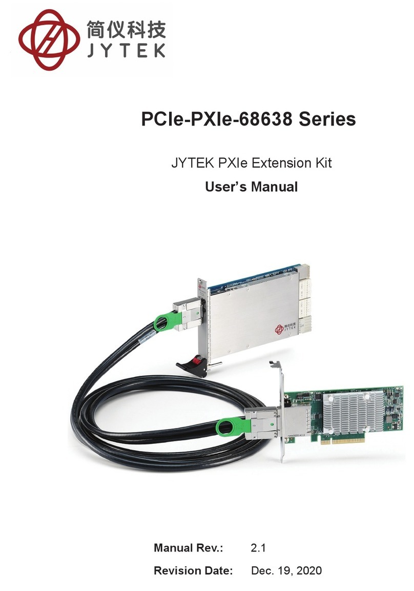
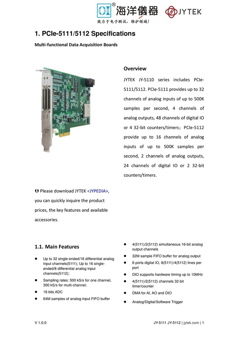
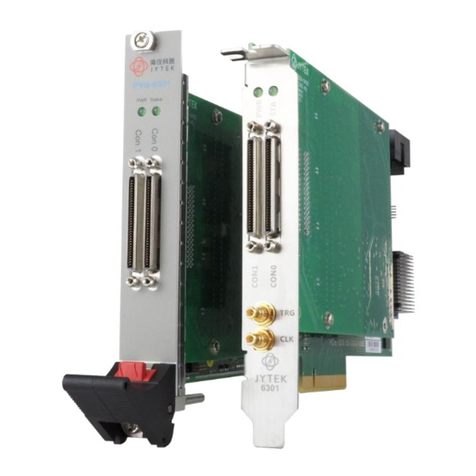
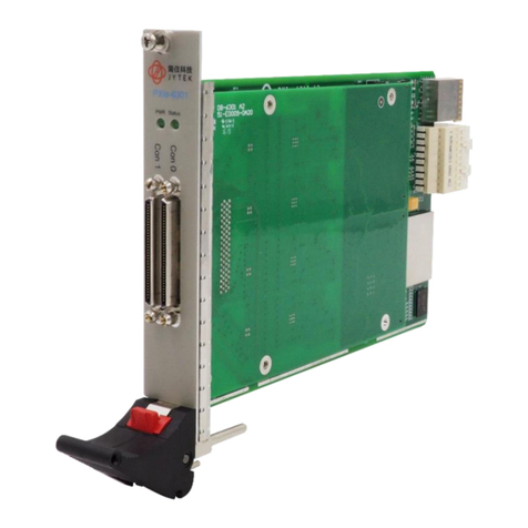
JYTEK PCI-69524 User manual

Advance Technologies; Automate the World.
Manual Revision: 1.00
Revision Date: Aug.26, 2017
PCI-69524
24-Bit Precision Load Cell Input Card
User’s Manual

ii

Preface iii
Preface
Copyright
This document contains proprietary information protected by copyright.
All rights are reserved. No part of this manual may be reproduced by any
mechanical, electronic, or other means in any form without prior
written permission of the manufacturer. All specifications are subject to
change without further notice.
Disclaimer
The information in this document is subject to change without prior
notice in order to improve reliability, design, and function and does not
represent a commitment on the part of the manufacturer.
In no event will the manufacturer be liable for direct, indirect, special,
incidental, or consequential damages arising out of the use or inability
to use the product or documentation, even if advised of the possibility
of such damages.
Environmental Responsibility
JYTEK is committed to fulfill its social responsibility to global environ-
mental preservation through compliance with the European Union's
Restriction of Hazardous Substances (RoHS) directive and Waste Electri-
cal and Electronic Equipment (WEEE) directive. Environmental protec-
tion is a top priority for JYTEK. We have enforced measures to ensure
that our products, manufacturing processes, components, and raw
materials have as little impact on the environment as possible. When
products are at their end of life, our customers are encouraged to dis-
pose of them in accordance with the product disposal and/or recovery
programs prescribed by their nation or company.
Trademarks
PC, PS/2, and VGA are registered trademarks of International Business
Machines Corp. Borland®, Borland® C, C++ Builder®, and Delphi® are
registered trademarks of the Borland Software Corporation. Microsoft®,
Visual Basic®, Visual C++®, Windows® 98, Windows® NT, Windows® 2000,
Windows® XP, and Windows® Vista® are registered trademarks of
iv Preface
Microsoft® Corporation. PCI™, is a registered trademark of the
Peripheral Component Interconnect Special Interest Group (PCI-SIG).
Product names mentioned herein are used for identification purposes
only and may be trademarks and/or registered trademarks of their
respective companies.

Preface v
Using this Manual
Audience and Scope
The PCI-69524 User’s Manual is intended for hardware technicians and
systems operators with knowledge of installing, configuring and
operating industrial grade PCI cards.
Manual Organization
This manual is organized as follows:
Preface: Presents important copyright notifications, disclaimers,
trademarks, and associated information on the proper
understanding and usage of this document and its associated
product(s).
Chapter 1, Introduction: Introduces the PCI-69524, its features,
applications, specifications and operating software environment.
Chapter 2, Installation: Describes how to install the PCI-69524 into
your chassis and basic PCI configuration settings.
Chapter 3, Signal Connections: Describes signal connections
between PCI-69524 and external devices.
Chapter 4, Operation Theory: Describes A/D and D/A conversions,
pulse-commands, encoder inputs and isolated digital I/O signals to
assist users in understanding how to configure and program the
cPCI-69524.
Chapter 5, Calibration: Presents the calibration process to minimize
measurement and output errors.
Important Safety Instructions: Presents safety instructions all users
must follow for the proper setup, installation and usage of
equipment and/or software.
Warranty Information: Presents important warranty information for
users/manufacturers rights and responsibilities regarding JYTEK
products and services.
Getting Service: Contact information for JYTEK’s worldwide offices.

vi Preface
Conventions
Take note of the following conventions used throughout this manual to
make sure that users perform certain tasks and instructions properly.
NOTE:
NOTE:
Additional information, aids, and tips that help users perform
tasks.
CAUTION:
Information to prevent minor physical injury, component
damage, data loss, and/or program corruption when trying to
complete a task.
WARNING:
Information to prevent serious physical injury, component
damage, data loss, and/or program corruption when trying to
complete a specific task.

Table of Contents vii
Table of Contents
Preface .......................................................................................... iii
Table of Contents.......................................................................... vii
List of Figures................................................................................. xi
List of Tables ................................................................................ xiii
1 Introduction.............................................................................. 1
1.1 Features ......................................................................................... 2
1.2 Applications ................................................................................... 2
1.3 Specifications ................................................................................. 3
1.4 Software Support......................................................................... 19
2 Getting Started ....................................................................... 21
2.1 Installation Environment ............................................................. 21
2.2 Package Contents ........................................................................ 22
2.3 PCI-69524 Layout......................................................................... 23
2.4 Installing the Card........................................................................ 24
2.5 PCI Configuration ......................................................................... 25
3 Signal Connections .................................................................. 27
3.1 Connectors & Pin Assignments.................................................... 27
3.2 Analog Input Signal Connections ................................................. 33
3.2.1 Signal Sources....................................................................33
3.2.2 Input Configurations..........................................................33
3.3.1 Signal Sources and Terminal Devices.................................38
3.3.2 Connecting to/from External Encoders .............................40
3.3.5 Interfacing Isolated DI with External Devices....................45
4 Operation Theory.................................................................... 47
4.1 PCI-69524 Function Diagram ....................................................... 47

viii Table of Contents
4.2 Analog Input Channels................................................................. 48
4.2.1 Signal Acquisition and Processing Flow............................. 48
4.2.2 How to Define a 1 in 200,000 Count Resolution ............... 49
4.2.3 Data Rate versus Sampling Rate........................................ 51
4.2.4 Auto-scan, Multiplexing and Settling Time ....................... 51
4.2.5 Power Line Noise Rejection............................................... 53
4.2.6 Excitation and Remote-sensing......................................... 54
4.2.7 Thermal EMF, 1/f Noise and Auto-zero............................. 54
4.2.8 Warm-up Requirement ..................................................... 57
4.2.9 Post-processing IIR Digital Filter........................................ 57
4.2.10 RAW Data Format ............................................................. 60
4.2.11 AD Data Format................................................................. 61
4.2.12 Data Transfer Modes......................................................... 63
4.2.13 Trigger Modes ................................................................... 64
4.3 D/A Conversion ........................................................................... 65
4.4 Isolated Encoder Input Channels................................................. 66
4.5 Isolated Pulse-Command Generator ........................................... 67
4.6 Isolated Digital I/O....................................................................... 68
4.6.1 Isolated Digital Inputs ....................................................... 68
4.6.2 Isolated Digital Outputs .................................................... 68
4.7 Trigger Sources............................................................................ 69
4.7.1 Software-Trigger ............................................................... 69
4.7.2 External Digital Trigger...................................................... 69
4.7.3 Pulse Comparator Trigger ................................................. 70
4.7.4 Position Comparator Trigger............................................. 71
5 Calibration ............................................................................... 73
5.1 Loading Calibration Constants..................................................... 73
5.2 Auto-calibration........................................................................... 74
5.3 Saving Calibration Constants....................................................... 74
Important Safety Instructions ....................................................... 75

List of Figures xi
List of Figures
Figure 1-1:PCI-69524 Product Image...............................................................1
Figure 1-2:Effective-number-of-bits vs. Gain...................................................9
Figure 1-3:RMS Noise in µV vs. Gain................................................................9
Figure 1-4:Spectral Response ±10 V range,
0.996094 kHz sine wave, -1 dB FS ...........................................10
Figure 1-5:Spectral Response ±5 V range,
0.996094 kHz sine wave, -1 dB FS ...........................................10
Figure 1-6:Spectral Response ±2.5 V range,
0.996094 kHz sine wave, -1 dB FS ...........................................11
Figure 1-7:Spectral Response ±1.25 V range,
0.996094 kHz sine wave, -1 dB FS ...........................................11
Figure 1-8:Frequency Response Sampling at 30,000 SPS ..............................12
Figure 1-9:Frequency Response Sampling at 15,000 SPS ..............................12
Figure 1-10:Frequency Response Sampling below 15,000 SPS .....................13
Figure 2-1:PCI-69524 PCB Layout and Mechanical Drawing..........................23
Figure 3-1:CN1 Connector & Pin Assignments...............................................28
Figure 3-2:CN2 Connector & Pin Assignments...............................................29
Figure 3-3:SSI Connector & Pin Assignments.................................................30
Figure 3-4:Connecting to a four-terminal load-cell transducer using a four-wire
connection ..............................................................................34
Figure 3-5:Connecting to a six-terminal load-cell transducer using a six-wire con-
nection ....................................................................................35
Figure 3-6:Connecting to a four-terminal load-cell transducer using a six-wire
connection ..............................................................................36
Figure 3-7:Ground-referenced source and differential input........................36
Figure 3-8:Floating source and differential input ..........................................37
Figure 3-9:Connecting to an external encoder with NPN sink drivers...........40
Figure 3-10:Connecting to an external encoder with PNP source drivers.....40
Figure 3-11:Connecting to an external encoder with push-pull source drivers41
Figure 3-12:Connecting to an external encoder with differential line-drivers41
Figure 3-13:Connecting to an external servo-amplifier with opto-coupler inputs
42
Figure 3-14:Connecting to an external servo-amplifier with differential line-re-
ceivers .....................................................................................42
Figure 3-15:Connecting to an external resistive load from the isolated DO sink
driver .......................................................................................43
Figure 3-16:Connecting to an external inductive load from an isolated DO sink
driver .......................................................................................44

xii List of Figures
Figure 3-17:Connecting to a low-side push button....................................... 45
Figure 3-18:Connecting to an external sink driver ........................................ 46
Figure 4-1:PCI-69524 Function Diagram ....................................................... 47
Figure 4-2:Signal acquisition and data processing flow
for transducer input channels................................................. 48
Figure 4-3:SINC Filter Power Line Noise Rejection
at 60 Hz Multiples ................................................................... 53
Figure 4-4:The Effect of Auto-zero on Thermal Noise and
1/f Noise, ADC running at 60 SPS............................................ 56
Figure 4-5:Digital Filter Tap Length Effects
on Signal Frequency Responses.............................................. 58
Figure 4-6:Linked List of PCI address DMA descriptors................................. 64
Figure 4-7:Post trigger................................................................................... 65
Figure 4-8:X4 Encoder mode......................................................................... 67
Figure 4-9:External digital trigger.................................................................. 70

List of Tables xiii
List of Tables
Table 1-1:-3dB small signal bandwidth: (Typical, 25°C)..................................4
Table 1-2:System Noise (including Quantization, Typical, 25°C) ....................4
Table 1-3:Transducer Input Impedance..........................................................5
Table 1-4:Transducer CMRR (DC to 60 Hz, Typical 25°C)................................5
Table 1-5:Settling Error: (Typical, 25°C)..........................................................6
Table 1-6:Programmable input range and gain ..............................................7
Table 1-7:-3dB small signal bandwidth vs. input range ..................................7
Table 1-8:-3dB small signal bandwidth vs. sampling rates,
in ±10V range ............................................................................8
Table 1-9:General Purpose Input Impedance...............................................13
Table 1-10:General Purpose CMRR (DC to 60 Hz, Typical, 25°C) ..................13
Table 1-11:Settling Error: (Typical, 25ºC) .....................................................14
Table 3-1:I/O Signal Descriptions..................................................................31
Table 4-1:Data Rates vs. Multiplexing, Auto-zero &
ADC Sampling Rates, in Samples-per-second (SPS).................52
Table 4-2:Temperature Coefficient of different metal junctions .................55
Table 4-3:Default Threshold Values (ADC counts) vs. ADC Sampling Rates .60
Table 4-4:RAW Data Format .........................................................................60
Table 4-5:Bipolar analog input ranges and
output digital codes for transducer input channels................62
Table 4-6:Bipolar analog input ranges and
AD codes for general purpose input channels ........................62
Table 4-7:Bipolar output code table.............................................................66

xiv List of Tables
This page intentionally left blank.

Introduction 1
1 Introduction
The JYTEK PCI-69524 is a 24-bit high-resolution multifunction DAQ card
capable of up to 30 kS/s sampling rate, providing 4-CH load-cell trans-
ducer input channels, and 4-CH general purpose analog input. In addi-
tion, the PCI-69524 comes with a 2-CH 16-bit analog output, isolated
motion I/O and digital I/O. The highly integrated function makes the PCI-
69524 the ideal solution for combined data acquisition and motion con-
trol functionalities. Ideal for manufacturing, laboratory research, and
factory automation, the PCI-69524 comes with all the features and per-
formance you need at an affordable price.
Figure 1-1: PCI-69524 Product Image

2 Introduction
1.1 Features
PCI-69524 24-bit multifunction DAQ card provides the following
advanced features:
Supports 32-bit 3.3 V or 5V PCI bus
Load-cell transducer input channels
4-CH differential analog input with remote-sense
4-CH transducer excitation, 10 V or 2.5 V selectable
Auto-zero capability
Up to 30 kS/s sampling rate without auto-zero
IIR digital filter for post-processing
General purpose analog input channels
4-CH differential analog input
Programmable gains: x1, x2, x4, x8
Up to 30 kS/s sampling rate
2-CH 16-bit analog output
3-CH opto-isolated pulse-command output, supporting CW/CCW,
CLK/DIR modes
3-CH opto-isolated encoder input, supports AB phase inputs in
quadrature mode
8-CH opto-isolated digital inputs
8-CH opto-isolated digital outputs with N-MOS sink drivers
Auto-calibration
1.2 Applications
Materials Testing Systems
Precision Weighting Systems
Automotive Testing
Process Control
Laboratory Automation
Biotech Measurements

Introduction 3
1.3 Specifications
Analog Input (AI) for Transducers
Number of channels: (programmable)
4 differential inputs (DI)
A/D converter:
ADS1255
Maximum sampling rate:
Without Auto-zero
30,000 samples/s (single channel)
1,638 samples/s (multiplexed/scanning)
With Auto-zero
819 samples/s (single channel or multiplexed/scanning)
Resolution:
24-bit
Input coupling: DC
Input range and gain:
±200 mV relative to a common-mode input voltage
A fixed gain of 25x
Operational common-mode input range:
-2 V to +6 V
Transducer Excitation Voltage Sources:
4-CH differential output
10 V or 2.5 V selectable (all 4-CH share same settings)
Driving up to four 120-ohm load-cells
Short-circuit protection
Remote-sense input:
4-CH differential input
0 V to 10 V operating input range
Overvoltage protection:
Transducer inputs
Power on: +28.7 V to -35.7 V (continuous)
Power off: ±15 V (continuous)

4 Introduction
Remote-sense inputs:
Power on: -40 V to +55 V (continuous)
Power off: -40 V to +55 V (continuous)
FIFO buffer size: 1024 samples (1024 x 32 bits)
Data transfers:
Programmed I/O
Bus-mastering DMA with scatter/gather
Table 1-1: -3dB small signal bandwidth: (Typical, 25°C)
Table 1-2: System Noise (including Quantization, Typical, 25°C)
Input Range Bandwidth (-3dB)
±200 mV 2,730 Hz
Input
Range
Data Rate
in SPS
System
Noise in
LSBrms
RMS Res.
in Bits
(ENOB)
Peak Res.
in Bits
RMS Res
in µV
Peak Res.
in µV
±200 mV
1.25 0.5 23.0 21.0 0.013 0.053
2.5 0.6 22.8 20.4 0.014 -0.079
5.0 0.6 22.7 20.4 0.016 0.079
7.5 0.7 22.6 20.0 0.017 0.079
12 0.9 22.2 19.7 0.023 0.159
15 0.8 22.3 19.7 0.020 0.132
24 1.2 21.8 19.2 0.031 0.212
29 1.1 21.9 19.0 0.030 0.185
47 1.9 21.1 18.6 0.037 0.291
194 2.9 20.5 17.7 0.078 0.583

Introduction 5
Test conditions: Rice Lake Load-cell Simulator IV set at 0mV/V output,
10V excitation and six-wire remote-sense connection, auto-zero
enabled. The RMS resolution and peak resolution are calculated relative
to full-scale input range of ±200mV.
Table 1-3: Transducer Input Impedance
Table 1-4: Transducer CMRR (DC to 60 Hz, Typical 25°C)
±200 mV
316 3.7 20.1 17.1 0.101 0.742
463 5.5 19.6 16.4 0.146 1.113
595 6.9 19.2 16.4 0.185 1.351
704 8.9 18.9 15.9 0.243 1.748
768 10.9 18.6 15.5 0.306 2.305
819 12.6 18.4 15.4 0.328 2.331
Normal Power On Power Off Overload
1 G || 3 pF 1 K1 K
Input Range CMRR
±200 mV 90 dB (Auto-zero Disabled)
102 dB (Auto-zero Enabled)
Input
Range
Data Rate
in SPS
System
Noise in
LSBrms
RMS Res.
in Bits
(ENOB)
Peak Res.
in Bits
RMS Res
in µV
Peak Res.
in µV

6 Introduction
Table 1-5: Settling Error: (Typical, 25°C)
Time-base source: Internal 40 MHz
Trigger mode: post-trigger
Offset error:
Before calibration: ±0.5 mV typical
After calibration: ±0.001 mV typical (auto-zero disabled), <
±0.001 mV typical (auto-zero enabled)
Transfer Linearity:
Better than: ±0.0035% over full-scale input range
Gain error:
Before calibration: ±1% typical
After calibration: ±0.5% typical
Analog Input (AI) for General Purpose
Number of channels: (programmable)
4 differential input (DI)
A/D converter:
ADS1255
Maximum sampling rate:
30,000 samples/s (single channel)
1.638 samples/s (multiplexed/scanning)
Resolution:
24-bit
Input coupling: DC
Input Range Condition Settling Error
±200 mV Scanning 200 mV step max 0.01%
Table of contents
Other JYTEK Computer Hardware manuals

JYTEK
JYTEK PCIe-5111 User manual

JYTEK
JYTEK PCIe-6301 Series User manual

JYTEK
JYTEK USB-62405 User manual

JYTEK
JYTEK PCIe-68638 Series User manual

JYTEK
JYTEK 6743X Series User manual

JYTEK
JYTEK USB-62401 User manual

JYTEK
JYTEK PCIe-68560 User manual

JYTEK
JYTEK NuDAQ PCI-69222 User manual

JYTEK
JYTEK PCIe/PXIe-6301 Series User manual

JYTEK
JYTEK JY-5110 Series User manual