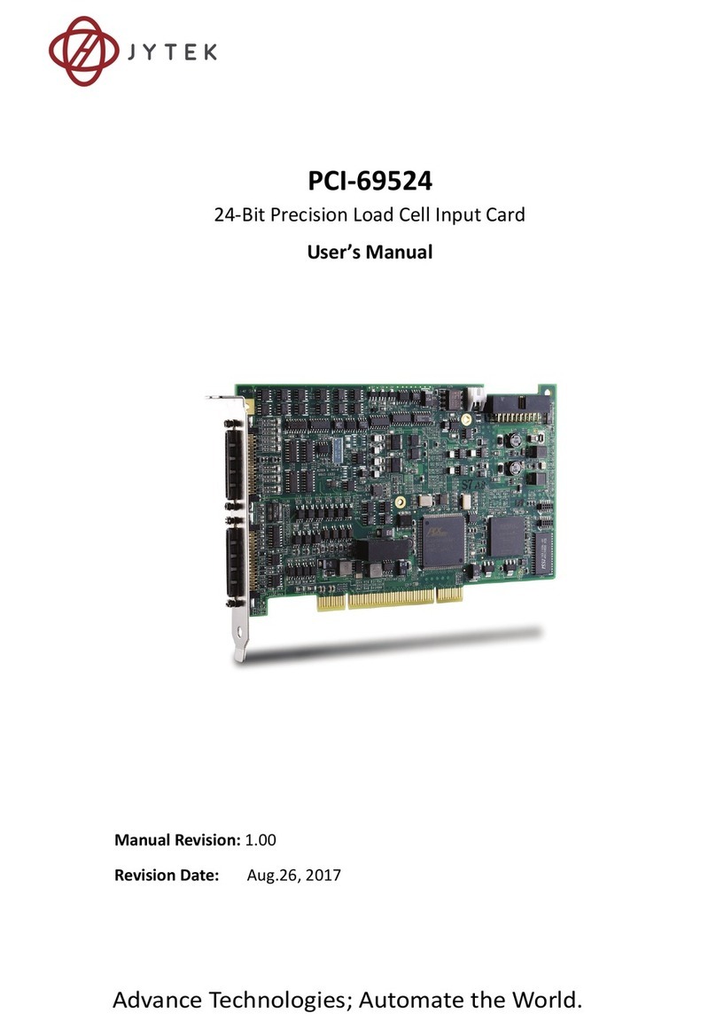
JYTEK NuDAQ PCI-69222 User manual

Advance Technologies; Automate the World.
Manual Rev. 1.00
Revision Date: May 30, 2017
NuDAQ® PCI-69222
NuDAQ® PCI-69223
16-bit High-Performance DAQ Card with
Programmable Function I/O
User’s Manual

Using this manual
1.1 Copyright
This document contains proprietary information protected by
copyright. All rights are reserved. No part of this manual may be
reproduced by any mechanical, electronic, or other means in any
form without prior written permission of the manufacturer. All
specifications are subject to change without further notice.
1.2 Audience and scope
This manual guides you when using JYTEK high-performance
data acquisition PCI card. The card’s hardware, signal connec-
tions, and calibration information are provided for faster applica-
tion building. This manual is intended for computer programmers
and hardware engineers with advanced knowledge of data acqui-
sition and high-level programming.
1.3 How this manual is organized
This manual is organized as follows:
Chapter 1 Introduction: This chapter introduces the JYTEK
NuDAQ PCI-69222 and NuDAQ PCI-69223 cards including
their features, specifications, software support information, and
package contents.
Chapter 2 Hardware Information: This chapter presents the
card’s layout, connector pin assignment, signal descriptions,
and analog input signal connection.
Chapter 3 Installation: This part describes the PCI-69222/
PCI-69223 installation and configuration.
Chapter 4 Operation Theory: The operation theory of the
PCI-69222/PCI-69223 card functions are discussed in this
chapter. These include A/D conversion, D/A conversion, pro-
grammable function I/O, application function I/O, digital wave-
form acquisition, isolation encoder, and trigger sources.
Chapter 5 Calibration: The chapter offers information on how
to calibrate the PCI-69222/PCI-69223 for accurate data acqui-
sition and measurement.

Warranty Policy: This presents the JYTEK Warranty Policy
terms and coverages.
Getting Service: Contact information for JYTEK’s worldwide
offices.
1.4 Conventions
Take note of the following conventions used throughout the man-
ual to make sure that you perform certain tasks and instructions
properly.
NOTE Additional information, aids, and tips that help you per-
form particular tasks.
IMPORTANT Critical information and instructions that you MUST perform to
complete a task.
WARNING Information that prevents physical injury, data loss, mod-
ule damage, program corruption, and others when trying
to complete a particular task.


Table of Contents i
Table of Contents
Table of Contents............................................................................ i
List of Tables .................................................................................. iii
List of Figures................................................................................. iv
1 Introduction.............................................................................. 1
1.1 Features ......................................................................................... 2
1.2 Applications ................................................................................... 2
1.3 Specifications ................................................................................. 3
1.4 Unpacking Checklist....................................................................... 8
1.5 Software Support........................................................................... 8
Driver Support for Windows ....................................................9
2 Hardware Information ............................................................ 13
2.1 Card Layout.................................................................................. 13
2.2 Connector Pin Assignment........................................................... 13
CN1 Pin Assignment ...............................................................14
CN2 Pin Assignment ...............................................................16
CN1/CN2 Signal Descriptions .................................................17
SSI Connector Pin Assignment ................................................18
SSI Connector Signal Description ...........................................19
2.3 Analog Input Signal Connection................................................... 20
Types of Signal Sources ..........................................................20
Input Configurations ..............................................................21
3 Installation.............................................................................. 25
3.1 Before You Proceed ..................................................................... 25
3.2 Installing the Card........................................................................ 25
3.3 Configuring the Card.................................................................... 26
Configuration ..........................................................................26
Troubleshooting .....................................................................26
4 Operation Theory.................................................................... 27
4.1 Block Diagram .............................................................................. 27
4.2 A/D Conversion............................................................................ 28
AI Data Format .......................................................................29
Software Conversion with Polling Data Transfer

ii Table of Contents
Acquisition Mode (Software Polling) .......................... 30
Continuous Acquisition (Scanning) Mode .............................. 31
Trigger Modes ........................................................................ 34
Bus-mastering DMA Data Transfer ........................................ 36
4.3 D/A Conversion ........................................................................... 39
Bipolar Output Modes ........................................................... 39
Software Update .................................................................... 39
Waveform Generation ........................................................... 39
4.4 Programmable Function I/O........................................................ 48
TTL DI/DO ............................................................................... 48
General Purpose Timer/Counter ........................................... 49
Basic Timer/Counter Functions .............................................. 49
General Purpose Timer/Counter Modes ............................... 50
Digital Waveform Acquisition and Generation ...................... 56
4.5 Isolation Encoder......................................................................... 58
4.6 Trigger Sources............................................................................ 63
Software Trigger .................................................................... 63
External Digital Trigger ........................................................... 63
5 Calibration ............................................................................... 65
5.1 Loading Calibration Constants..................................................... 65
5.2 Auto-calibration........................................................................... 65
5.3 Saving Calibration Constants....................................................... 66
Warranty Policy ............................................................................ 67
Getting Service ............................................................................. 69

List of Tables iii
List of Tables
Table 2-1: CN1 Pin Assignment for PCI-69222 .................................. 14
Table 2-2: CN1 Pin Assignment for PCI-69223 .................................. 15
Table 2-3: CN2 Pin Assignment for PCI-69222/PCI-69223 ................ 16
Table 2-4: CN1/CN2 Signal Description ............................................ 17
Table 2-5: SSI Connector Pin Assignment ......................................... 18
Table 2-6: SSI Connector Signal Description ..................................... 19
Table 4-1: Bipolar Analog Input Range and Output Digital Code ..... 29
Table 4-2: Bipolar Analog Input Range and Output Digital Code ..... 29
Table 4-3: Bipolar Output Codes ...................................................... 39
Table 4-4: Summary of Counters for Waveform Generation ........... 41
Table 4-5: TTL DIO Pins in CN1 ......................................................... 48
Table 4-6: Timer/Counter Mode Pins in CN1 .................................... 49
Table 4-7: Encoder Pins in CN2 ......................................................... 58

List of Figures iv
List of Figures
Figure 1-1: JYTEK Software Support Overview ..................................... 9
Figure 1-2: DAQPilot Main Interface................................................... 10
Figure 1-3: DAQMaster Device Manager............................................ 10
Figure 1-4: Legacy Software Support Overview.................................. 11
Figure 2-1: PCI-69222/PCI-69223 Layout............................................ 13
Figure 2-2: Floating Source and RSE Input Connections..................... 21
Figure 2-3: Ground-referenced Sources and NRSE Input Connections 22
Figure 2-4: Ground-referenced Source and Differential Input ........... 23
Figure 2-5: Floating Source and Differential Input ............................. 23
Figure 4-1: PCI-69222/PCI-69223 Block Diagram ............................... 28
Figure 4-2: PCI-69222/PCI-69223 AI Circuitry..................................... 29
Figure 4-3: Continuous A/D Conversion Clock Source Block Diagram 31
Figure 4-4: Scan Timing....................................................................... 32
Figure 4-5: Post Trigger without Retrigger ......................................... 35
Figure 4-6: Post Trigger with Retrigger............................................... 35
Figure 4-7: Gated Trigger with Finite Scan Acquisition....................... 36
Figure 4-8: Scatter-gather DMA for Data Transfer ............................. 38
Figure 4-9: FIFO Data In/Out Structure............................................... 40
Figure 4-10: Waveform Generation for Three Channels Update ......... 40
Figure 4-11: Waveform Generation Clock Source Selection................. 41
Figure 4-12: Typical D/A Timing of Waveform Generation .................. 42
Figure 4-13: Post-Trigger Generation ................................................... 43
Figure 4-14: Delay-Trigger Generation ................................................. 44
Figure 4-15: Post-Trigger with Retrigger Generation ........................... 45
Figure 4-16: Finite Iterative Waveform Generation with Post-trigger . 46
Figure 4-17: Infinite Iterative Waveform Generation with Post-trigger 47
Figure 4-18: Mode 1 Operation ............................................................ 50
Figure 4-19: Mode 2 Operation ............................................................ 51
Figure 4-20: Mode 3 Operation ............................................................ 52
Figure 4-21: Mode 4 Operation ............................................................ 52
Figure 4-22: Mode 5 Operation ............................................................ 53
Figure 4-23: Mode 6 Operation ............................................................ 53
Figure 4-24: Mode 7 Operation ............................................................ 54
Figure 4-25: Mode 8 Operation ............................................................ 54
Figure 4-26: Mode 9 Operation ............................................................ 55
Figure 4-27: Mode 10 Operation
.......................................................................................... 55
Figure 4-28: Digital Waveform Acquisition Operation.......................... 57
List of Figures v
Figure 4-29: Digital Waveform Generation Operation ......................... 57
Figure 4-30: Encoder Isolation Input Module....................................... 58
Figure 4-31: Encoder OGRx Input ......................................................... 59
Figure 4-32: CW/CCW Encoder Timing ................................................. 59
Figure 4-33: X1 Encoder Mode ............................................................. 60
Figure 4-34: X2 Encoder Mode ............................................................. 60
Figure 4-35: X4 Encoder Mode ............................................................. 61
Figure 4-36: Phase Z.............................................................................. 62
Figure 4-37: External Digital Trigger ..................................................... 63

vi

Introduction 1
1 Introduction
The NuDAQ PCI-69222 (16-CH, 250 kS/s) and NuDAQ PCI-
69223 (32-CH, 500 kS/s) are 16-bit high-performance DAQ cards
with eight different input ranges. These cards also features a 2-
CH, 16-bit analog output capable of up to 1 MS/s update rate, a 2-
CH encoder input, and a programmable function I/O. The
software-programmable function I/O supports a variety of
applications including TTL digital I/O, high-speed DIO, general-
purpose timer/counter, and PWM output.
These cards’ analog input, analog output, and function I/O are
capable of functioning simultaneously at full speed. If you need
additional channels, you can synchronize these cards using the
onboard SSI (System Synchronization Interface) bus. Suitable for
mixed-signal tests, laboratory research, and factory automation,
the PCI-69222 and PCI-69223 provide the best single-board
solution with optimum integration capability of multiple tasks at an
affordable price.

2 Introduction
1.1 Features
The PCI-69222/PCI-69223 comes with the following features:
Supports a 32-bit 3.3 V or 5 V PCI bus
PCI 2.3-compliant
Up to 32-CH single-ended or 16-CH differential analog input
Up to 500 kS/s sampling rate
Programmable analog input gains of 1, 2, 4, 5, 8, 10, 20, 40
2-CH, 16-bit simultaneous analog output supports update
rate of up to 1 MS/s
Programmable function I/O supports the following modes:
16-CH TTL DI and 16-CH TTL DO
2 MHz 32-CH high-speed DIO
4-CH 32-bit 80 MHz general-purpose timer/counter
4-CH PWM outputs
2-CH 4 MHz dedicated encoder inputs, supporting AB
phase, and CW/CCW
Four DMA channels for A/D, D/A, and high-speed DIO
External digital trigger for A/D, D/A, and high-speed DIO
Multiple card synchronization through SSI (System Syn-
chronization Interface)
Auto-calibration feature
1.2 Applications
The PCI-69222 and PCI-69223 are ideal for these applications:
Automotive testing
Cable testing
Transient signal measurement
Waveform generation
ATE
Laboratory automation
Biotech measurement
Motor control feedback

Introduction 3
1.3 Specifications
Analog Input (AI)
Hardware PCI-69222 PCI-69223
Number of channels
(programmable) 16 32
A/D converter AD7685 or equivalent AD7686 or equivalent
Maximum sampling rate
Single-channel:
Scanning:
250 K samples/s
100 K samples/s
500 K samples/s
200 K samples/s
Resolution 16-bit
Input coupling DC
Programmable input range ±10 V, ±5 V, ±2.5 V, ±2 V, ±1.25 V,
±1 V, ±500 mV, ±250 mV
Operational common mode
voltage range ±8 V
Overvoltage protection
Power on:
Power off:
Continuous ±30 V
Continuous ±30 V
Continuous ±30 V
Continuous ±30 V
FIFO buffer size 1K samples
Data transfers Programmed I/O
Bus-mastering DMA with scatter/gather
Channel Gain Queue
configuration size 32 words
Input impedance 1000G/150pF
Trigger mode Post-trigger with retrigger, Gated trigger
Time-base source Internal, 80 Mhz
Electrical
Function 23°C (±5°C)
Offset error ±0.5 mV
Gain error ±2 mV
–3dB small signal bandwidth11.5 Mhz
System noise20.5 mVrms
1% THD large signal
bandwidth
CMRR393.5 dB

4 Introduction
Spurious-free dynamic range
(SFDR) 95 dB 88 dB
Signal-to-noise and distortion
ratio (SINAD) 86 dB 84 dB
Total harmonic distortion
(THD) –94 dB –90 dB
Signal-to-noise ration (SNR) 87 dB 86 dB
Effective number of bits
(ENOB) 13.9 13.5
Settling time to full-scale step
Multiple channels
Multiple ranges
2 µs to 0.1% error
4 µs to 0.01% error
Analog Output (AO)
Hardware
Function 23°C (±5°C)
Number of channels 2
D/A converter DAC8812 or equivalent
Maximum update range 1M sample/s (static)
Resolution 16-bit
FIFO size 512 samples, 2-CH sharing
Data transfers Programmed I/O, DMA
Output range ±10 V
Output coupling DC
Output impedance 0.010 (maximum)
Protection None
Stability Any passive load, up to 1500pF
Power-on state Around 0 V, steady-state
Electrical
Offset error
Before calibration:
After calibration:
±35 mV typical
±1 mV typical
Gain error
Before calibration:
After calibration:
±1% of output max
0.001% of output max
Slew rate 20 V/µs
Rise time 0.67 µs

Introduction 5
Fall time 0.7 µs
Settling time to 1% output
error 3 µs
DNL 0.7 LSB
INL 1 LSB
Output driving ±5 mA (maximum)
Function I/O
Number of channels • 16-CH programmable function DI
• 16-CH programmable function DO
Compatibility TTL (single-ended)
(supports 3.3 V and 5 V DI; 3.3 V DO)
Input voltage • Logic low: VIL=0.8 V max; IIL=0.2 mA max
• Logic high: VIH=2.0 V min; IIH=0.2 mA max
Output voltage
• Logic low: VOL=0.5 V max; IOL=10 mA max
• Logic high: VOH=2.6 V min; IIH=10 mA max
Supported modes4• 16-CH TTL DI and16-CH TTL DO
• 4-CH 32-bit general-purpose timer/counters
Clock source: Internal or External
Max. source frequency: Internal 80 MHz
External 10 MHz
• 4-CH PWM outputs
Duty cycle5:1-99%
Modulation frequency: 20 MHz to 0.005 Hz
• External digital trigger in and out
• External analog input convert source
• External analog output convert source
• Digital waveform acquisition and generation
DI acquisition FIFO size 512 samples
DO acquisition FIFO size 512 samples
Data transfers Programmed I/O, DMA

6 Introduction
1. -3dB small signal bandwidth: (Typical, 25ºC)
Encoder Input (EI)
Number of channels 2
Max. Input frequency 4 MHz
Encoder count (2³¹-1) bits
Photo isolator NEC PS9115 or equivalent
Encoder modes • CW/CCW
• X1 AB phase encoder
• X2 AB phase encoder
• X4 AB phase encoder
Physical, Power, and Operating Environment
Interface PCI 2.3-compliant
Dimension 120 mm x 87 mm
I/O connector 2 x 68-pin female VHDCI connectors
Power requirement (typical) • +5 VDC: 1.2A
• +12 VDC: 760 mA
• -12 VDC: 50 mA
Operating environment • Ambient temperature: 0ºC to 45ºC
• Relative humidity: 10% to 90%,
non-condensing
Storage environment • Ambient temperature: -20ºC to 80ºC
• Relative humidity: 5% to 95%,
non-condensing
Specifications are subject to change without notice.
Input range Bandwidth(-3dB)
±10 V 1500 kHz
±5 V 1400 kHz
±2.5 V 1400 kHz
±2 V 1400 kHz
±1.25 V 1400 kHz
±1 V 1400 kHz
±500 mV 1350 kHz
±250 mV 1250 kHz

Introduction 7
2. System Noise (LSBrms, including Quantization, Typical, 25 ºC)
3. CMRR (DC to 60 Hz, Typical)
4. Only one of the following modes can be selected. These
modes can not work at the same time. Refer to section
4.3 and 4.4.
5. Refer to Chapter 4.
Input Range System Noise
±10 V 0.78 LSBrms
±5 V 0.80 LSBrms
±2.5 V 0.98 LSBrms
±2 V 0.96 LSBrms
±1.25 V 0.77 LSBrms
±1 V 0.81 LSBrms
±500 mV 0.99 LSBrms
±250 mV 0.96 LSBrms
Input Range System Noise
±10 V 93.5 dB
±5 V 96.3 dB
±2.5 V 103 dB
±2 V 104.2 dB
±1.25 V 106 dB
±1 V 106.2 dB
±0.5 V 110 dB
±0.25 V 118 dB

8 Introduction
1.4 Unpacking Checklist
Before unpacking, check the shipping carton for any damage. If
the shipping carton and/or contents are damaged, inform your
dealer immediately. Retain the shipping carton and packing mate-
rials for inspection. Obtain authorization from your dealer before
returning any product to JYTEK.
Check if the following items are included in the package.
PCI-69222 or PCI-69223 multi-function DAQ card
If any of the items is damaged or missing, contact your dealer
immediately.
CAUTION The card must be protected from static discharge and
physical shock. Never remove any of the socketed parts
except at a static-free workstation. Use the anti-static bag
shipped with the product to handle the card. Wear a
grounded wrist strap when servicing.Software Support
1.5 Software Support
JYTEK provides comprehensive software drivers and packages to
suit various user approach to building a system. Aside from pro-
gramming libraries, such as DLLs, for most Windows-based sys-
tems, JYTEK also provides drivers for other application
environment. JYTEK also provides ActiveX component ware for
measurement and SCADA/HMI, and breakthrough proprietary
software applications.
All software options are included on the website: http://
www.jytek.com.

Introduction 9
Figure 1-1: JYTEK Software Support Overview
Driver Support for Windows
DAQPilot
DAQPilot is a driver and SDK with a graphics-driven interface
for various application development environments. DAQPilot
comes as JYTEK's commitment to provide full support to its
comprehensive line of data acquisition products and is
designed for the novice to the most experienced programmer.

10 Introduction
Figure 1-2: DAQPilot Main Interface
As a task-oriented DAQ driver, SDK and wizard for Windows
systems, DAQPilot helps you shorten the development time
while accelerating your learning curve for data acquisition pro-
gramming.
You can download and install DAQPilot at
http://www.jytek.com.
DAQMaster
The JYTEK DAQMaster is a smart device manager that opens
up access to JYTEK data acquisition and test and measure-
ment products. DAQMaster delivers all-in-one configurations
and provides you with a full support matrix to properly and con-
veniently configure JYTEK Test and Measurement products.
Figure 1-3: DAQMaster Device Manager
As a configuration-based device manager for JYTEK DAQ
cards, DAQMaster enables you to manage JYTEK devices and
interfaces, install and upgrade software applications, and man-
age JYTEK DAQPilot tasks.
This manual suits for next models
1
Table of contents
Other JYTEK Computer Hardware manuals

JYTEK
JYTEK 6743X Series User manual

JYTEK
JYTEK JY-5110 Series User manual

JYTEK
JYTEK USB-62401 User manual

JYTEK
JYTEK PCIe-68638 Series User manual

JYTEK
JYTEK USB-62405 User manual

JYTEK
JYTEK PCIe-5111 User manual

JYTEK
JYTEK PCIe-6301 Series User manual

JYTEK
JYTEK PCIe/PXIe-6301 Series User manual

JYTEK
JYTEK PCIe-68560 User manual

JYTEK
JYTEK PCI-69524 User manual