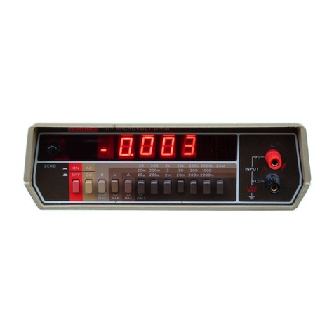
Keithley 171 User manual

Instruction Manual
Model 171
Digital Multimeter
01997, Keithley Instruments, Inc.
Cleveland, Ohio, U.S.A.

KEITHLEY INSTRUMENTS. 1 N C.
INSTRUCTION MANUAL
MODEL 171
DIGITAL MULTIMETER

CONTENTS
SECTION PAGE SECTION PAGE
Title Page ................ 1
contents ................. ii
IAt of Illusfratlons. .......... iii
specifications ............... iv
1. General Description
1-1. Inrraduceion .......... 1
1-2. warranty InformLion ...... 1
1-3. Change Notice. ......... 1
1-4. Features ............ 1
2. operation
2-1. Measurement Considerations ... :2-2. Ca**ecfianB. ...........
2-3. Controls ............ 5
2-4. Digital Display. ........ 5
2-5. operation 88 a Voltmeter .... 5
2-6. operaeion as an Amnlerer. ....
2-7. Operation as an Ohmmeter .... 2
2-8. Overloade. ...........
2-9. Digital Outputs and Controls . . z
2-10. Operating Technique. ...... 10
3. Circuit Description
3-1. General. ............ 13
3-2. Analog Amplifier ........ 13
3-3. Switching. ........... 14
3-4. Driven Guard Amplifier ..... 15
3-5. Protection ctrc"its. ...... 15
3-6. F"ncfion and Range Display ... 15
3-7. Digital Section. ........ 15
3-8. Power supply .......... 18
4. Accessories
4-l. General. ............ 20
4-2. operating Instructions ..... 20
4-3. Model 1712 w@al output. ... 20
4-4. Model 1713 Extender Card .... 20
4-5. Model 1007 Dual Rack Mounring Kit 20
4-6. Model 2000 Rack Mounting Kit . . 21
5. Maintenance
5-1. General. ............. 27.
5-2. Required Test Equipme. ..... 22
5-3. Performance Checks ........ 22
5-4. Adjustment and C.¶libration .... 26
5-5. Component and Calibration Layouts. 34
6. Replaceable Parts
6-1. General. ............. 40
6-2. EleCtrical schematics and Diagrams 40
6-3. HOWto "se the Parts List. .... 40
6-4. How to Order Parts ........ 40
6-5. Chassis Paru List ........ 41
6-6. Electrical Part* I&r. ...... 41
6-7. Mechanical Parts List. ...... 61
6-8. Code-to-Name List. ........ 68
7. Schematic Diagrams
7-1. 25532C Block Diagram. ...... 70
7-2. 24866D Optional BCD Output,
Model 1712. .......... 71
7-3. 248731) Tube Board (PC-299). ... 72
7-4. 25017D integrator Board (K-301). 73
7-5. 250980 Interconnect/Clock Board
(PC-300). ........... 74
7-6. 25130D Input Switching and Currenr
/Ohms Protection. ....... 75
7-7. 25131C AC Voltage Divider .... 76
7-8. 25132C Analog Switching ..... 77
7-9. 25133C Ohms Converter ...... 78
7-10. 2552% A.C. Converter ...... 79
7-11. 25529D Analog Amplifier ..... 80
7-12. 2553OD Power Supply ....... 81
7-13. 25531D Switching Decimal Point &
Function L&play. ....... 82
773

I
MODEL171
ILLUSTRATIONS
Figure
NO. Title Page
1 Model 171 Digifal Multimeter 1
2 Front Panel Controls and Terminals 2
3 Rear Panel Controls and Connectors 3
4a Complete Digital Display 5
4b Typical Display Reading 5
5 Digital OutpUt connector 7
6 output Buffer stage 8
7 Timing Diagram 9
8 Overall Block Diagram 12
9 Analog Amplifier 13
10 Active AC Divider 13
11 AC/DC converter 14
12 Ohmmeter Configuraria" 14
13 "olcmeter Co"f*g"rat*o" 14
14 Ammeter Configuration 15
15 Analog-to-Digital Converter 17
16 A-to-D Converter Block Diagram 19
17 Model 1007 Dual Rack Mounting Kit - Exploded View 21
18 Model 2000 Rack Mounting Kit - Exploded View 21
19 Cutaway View Showing PC-Board Locations 23
20 calibration ~djusmenrs and Tesr Points &Cal Cover 32
21 Calibration Adjustments and Test P"ints without Cover 33
22 Component Layout - Analog Board - PC-303 34
23 Companent Layouf - Clock B"ard - PC-300 34
24 Camponenr Layout - Mother Bonrd - PC-305 35
25 Component Layout - Switch Board - PC-304 36
26 component Layout - Integrator Board - PC-301 37
27 Componene Layout - Tube Board - PC-299 38
28 Caponent payout - Optional Digital Oufput - PC-275 39
29 Chassis Assembly - Exploded View 42
30 Bg<fom Cover Assembly - Exploded View 42
I
773

SPEClPICATlONS
SPECIFICATIONS
calibrated at 25°C
AS A DC “OLTMETEK
ACCURACY (90 days):
RANGE: ~1~1micro"olt per digit (1" rn" full range) to I"-100" range ~1.(0.3% OF reading +0.04% of range) 40
i”“Ltiples.
cMl2.R: GrcnCer than 100 d8 wit,, 1 kilohI ““balance,
dc t” 180 ,,z at 10 LLZmultiples.
MAx1nlM SAFE INPUT: ~I-1400volts peak nlomentary, 1000
v dc or rms ac C”“tin”““S.
AS A UC AMMETER
Rmm: LO.1 nanLmn,>ere per digit (IpA full range) to
~+2amperes in Se"en decade ranges.
T"g LO 19999 0" all ranges. 100% overrang-
ACC"P.ACY (90 days) : ~(0.05% Of reading +0.02% Of
range). SelI heating due to long term application
"f 2 amperes will callse less than 0.1% addirional
error 0" the l-ampere range.
TEMPE‘UT"RC cOEPFICIENT: +(".005% of readine +0.002%
to-19999 on a11
jl
ranges.
ACCUKACY (90 days:
j: ,o.OS% oc reading ior l-kilohm
through l-megohm ranges; 20.2% of reading 0” LiW
IO-merohm ranees: ,1.3%Of readine a1 the 1"o-meeohm
range; +20% or reading on the lOOO-megohm *ange
(?0.02% Of range an all ranges).
TEMPEKATURECOEFFICIENT: +(0.008% of reading +o.oo?.%
of ranee ~+0.0003% of readine r,er memhm~/"C.
SETTLING-TIME: Less than 2 &bnds t: raGI accuracy
VOLTAGEACROSS UNKNOWN: 100 mv for full range on the
l-kilohm to 100.kilohm ranges, 1" "aximum open cir-
CUIL. 1 Volt for full range 0" rtle I-megotrm eo
1000~megohm ranges, 5 volts open circuit.
MAxIMuM 0"EKLOA": 250 volts rms on the l"O-kihhm to
1000-meg"hm ranges. Diode clamped to protect the 1
and lo-kilohm ranges (internallr fused beyond 3 amps
AS AN AC "OLTMETEK
RANGE: 10 micro"olts per digit (100 nl" full range)
to 1000 vo1rs rms in five decade ranges. 100% aye*-
ranging to 19999 on all except the lOOO-volt range.
and I” ranges
lk” rance +(0.4% of readinr .+0.04% Of ranee, 40 HZ-
(Average reading, calibrated in rms of a sine wave.
TEMPERAT"KE COEFFICIWT: L10.35% of reading f0.003%
Of range (0.008% 0" 100-d range)l/"C.
INPUT IMPEDhNCE: i Ml> shunted by a,>proxi,,,ately 100 pl
SETTLING TIM?: Less than 3 seconds except for ac
superimposed on dc.
MAXIMUMSAFE INPUT: 1000.volts dc or rms ac (1500
volts peak) lo-"olc to 100".volt range, 300 volts
rms (450 volts "eak) a" the loo-Ill" and l-volt ranee:
AS AN AC AMMETEK
RANGE: 0.1 nanoampere per digit (I$ full range) to
2 amperes rms, In seven decade ranges. 100% over-
ranging to 19999 00 all ranges.
ACCURI\CY (90 days): ?(1.5% of reading +o.l% of range
40 Hz to 1OkHz on the LOO-microampere to l-ampere
ranges, decreasing to 40 117.to 200 Hz on the l-
microampere range (average reading, calibrated ii,
rms Of a sine wave).
TEMPERhTURECOEFFKIENT: +~(0.04% of reading +o.oo*%
the low* ranges increasing to approximately so0
millivolts on the l-ampere range.
MAxnluM SAFE INPUT: 3 amperes, internally fused
bewnd 3 amperes.
ZERO STAbILITY: ~(0.0005% "f range ~t0.3 ~V)/OC.
ANALOG OUTPUT: ,l vclt at up 1'3 1 mi1ii.ampere ior
full ranjz,e input, 100% o"erra"gi"y ora a11 ranqes
except tie lobe-volt ranges.
POLARITY: Automatic.
OFFSET C”RmNT: Typically less than 10 picoamperes.
DISPLAY: 4 digits plus 1 overrange digit; appropriate
decimal location; function in engineering units;
polarity and overload indicarion; 2 readings/second.
ISOLATION: Circuit ground to chassis ground: greater
than 100 megoihms shunted by Less than 0.02 micro-
farad. Circuit ground may be Eloaced up co 500 volt
with respect to chassis ground in all modes. Maxim"
safe voltage between input and chassis ground: 1500
volts peak.
WARMUPTIME: 45 minutes co within twice soecified
CONNECTORS: Input, chassis ground; binding posts.
Analog OUtput; Amphenol 80-PC2F.
POWER: 105-125 or 210-250 volts (switch selecred),
50-6" HZ, 25 watts.
1
i.
3.
)
s
m
9
1 DIMENSIONS,WEIGHT: Style M 3-l/2 in. half-rack, over-
all bench size 4 in. high x 8-l/2 in. wide x 15-l/4
in. deep (100 x 217 x 385 mm). Net weight, 10 pound
(4,6 kg).
ACCESSORIES S"PPLIED: Mating OUtpUt connector, spare
input fuse.
iv
773

I MODEL171
SECTION 1. GENERAL DESCRIPTION
773

General Description Paragraph
Turns on instrument power 2-3a
sets dc-voltage functian 2-3c
set.5 ac-voltage function 2-3c
sets ohms function 2-3c
Sets dc-ampere function 2-3c
sets ac-ampere function 2-3c
sets instrument sensiii.vity 2-3b
2-h
2-h
Z-2a

GENERAL “ESCKIPTION
TABLE l-2.
kar Panel Controls and Connectors
FUSE 117”: l/2 ampere 2.LOa
234”: l/4 ampere
OUTPUT
BCD OUTP”T
LINE Input
Analog output, 1v for full range
Provides digital outputs with Model 1712 installed
as shown (connector not provided without Model 1712)
receptacle mates with 3-wire line cord
2-2h
2-9a
?-l&3
ZERO ANALOG SC0 LINE
ADJUST OUTPUT OUTPUT SWITCH
It723 5502 5108 s701
3

SECTION 2. OPERATION
b. Shielding.
1. Electric Fields. Shielding is usually neces-
say when the Fnstrument is in the presence of very
large a--c fields or when very sensitive meaS”rementS
are being made. The shields of the measurement
circuit and leads should be connected together to
ground at only one point. This provides a “tree”
configuration, “hid, minimizes graund loops.
3. Other Considerations.
a) Voltmeter Measurements. “se shielded input
leads when source resistances are greater than 1
Kilohm or when lang input cables are used.
b) current Measurements. on the IlLA and p.4
current ranges, no special shielding precautions
need be taken. However, on the I microampere
range, shielded input leads are recommended.
c) Resiseance Measurements. Shielding of input
leads and source are recommended for measurements
on the 10 megohm through 1000 megotm ranges to
prevent erroneous readings.
C. Floating. The circuit ground to chassis ground
isolation is greater than 100 megohms shunted by less
than 0.02 microfarad. Circuit ground may be floated
up to 2500 volts With respect to chassis ground in a11
modes. TO use the Model II1 for floating measurements,
disconnect the shorting link between the LO and CASE
terminals on the front panel.
d. Source Impedance. The Model 171 has an input
resietance of 10% on the 10 Ill” to 1-v ranges. The
loading error *or these ranges Will be less than 0.003%
(negligible with respect to full scale readings) when
the source resistance is 30 kilahm or less. On the
10 v to 1000 ” ranges, input impedance is greater than
10’s?. Loading error will be negligible when the source
resistance is less Lhan 300 duns.
2-2. CONNECTIONS.(refer to Figures 2 and 3)
a. Input. Three binding posts are provided on the
front panel for input connections. The terminals are
color coded as follows: red = input high, black =
input low, and green = chassis ground. The shorting
link should be connected between LO and CASE for
grounded operation. The link should be removed for
floating operation.

I I
- I 2 3
.4
5 mYI

Full Range Full Range overrange
sensitivity loisplay Display
1 kll x.9999 !d 1.9999 kn
10 k$l x9.999 w 19.999 kc!
100 k!2 X99.99 kll 199.99 kil
4 I Ml x.9999 m 1.9999 MC.
i 10 K\i x9.999 Mn 19.999,m
6 100 MC x99.99 Mn
199.99 Mfl
7 100” MS? x999.9 MS’ 1999.9 m
1 kg! 100 rn” 100 LPA 2v 10 liw
10 kQ 100 ln” 1” ilh 2v I ,lW
100 !42 100 tnv 1 VA zv 0.1 ,,w
1 Mli I” 1 !a 12 ” 1 uw
10 MC 1” 100 *ii 12 ” 0.1 $4
100 M 1” 10 nA 12 ” 0.01 ,,w
1000 Mli I, v 1nA 12 v 0.001 +I
I
6
a. General. With the optional Model 1712 Digital
Out,,ut, the Keithley 171 becomes a systems-oriented in-
strument with a flexible BCD 8-4-2-l output that may
be easily interfaced with many digital printers or
COlilpUte*S. This flexibility is due to the wide opera-
ting voltage levels of the buffer stages of the 1712.
These stages utilize “open collector” output transis-
tars thaf may be operated at c~,,mon DTL and TT,. “olt-
age levels as well as others up LO f12 volts. I”
addition, the Model 1712 has ar. exeensive list of
built-in features which include camplere timing out-
purs and remote controls. Eight strobe lines are
also provided. Each line controls 4 bits of OUtpUt
data, which allows the I,12 to be easily set up for
8,12, or 16-bit coqmters or other digital devices.
The 1712 can be ordered factory-installed in tht ?;I,
or purchased separately in kit form for field install-
ation. The Model 1712 includes an output-buffet module,
w-wired 50-pin receptacle (5108), wiring harnses,
and mating 50-pin connector (not wired).
C. OUtput Connector Pin Identification. Refer
to Table 2-7 and Figure 5. The 50-1>i” BCD-output
receptacle (5108) of the Mod<51 171 i.s arl Amphenol
Micro-Ribbon type 57-40500 (Ke*thle, 7 CS-221). The
supplied mating connector is an Amphenol Micro-
773
MODEL 171
TABLE 2-6.
Specifications
Model 1712 Digital output
1
OIGITAI. OUTPUT:
BCD (8421) open collector lo-
gic (Motorola MC 858P) represents each of 4
digits (0000=0), overrange digit, overload
(“l”), polarity (+ = “l”), function and four
decimal positions.
TIMING OUTPUTS: Clock: 100 kHz pulses.
CO”nf Interval: Logic “0” appears during
count interval (i.e. pulse width is propor-
tional to analog input signal). Flag (Fx):
Logic “1” (“0”) appears for a 300-m*ll*second
interval out of a co”“ers*o” time of 500
milliseconds. No change in digital output is
made during this interval.
OUTPUT LOGIC LEVELS: 0”fp”t Logic “1” - open
transistor collector to ground with leas
than 100 microamperes leakage. +12 volts
maximum allowable applied voltage. output
Logic “0” : transistor switch closure to
ground with less than 0.5-volt saturation
voleage at f35 milliamperes sink current.
REMOTE CONTROLS: a: 8 lines permit
ward serializina in 4-bit increments or
multiples thereof. “pen circuit inhibita
controlled output lines from conducting
(closure enables conduction). Hold:
Closure retains result of last con”ersion
in both the digital output and the display.
Hold 112: Closure hairs co”“ersions at
end of present conversion holding reading
in bath the digital outpuf and the dis-
play. w: Release edge of pulsed
closure initiates one con”ers*o” when in
Hold 112. Signal is averaged for a ZOO-
nrillisecond period starting 100 milli-
seconds after release of “Trifiger” or
Hold 112. Flag Reset: Closure sets
Flag (Flag) to logic “0” (“1”).
mqumm CONTROI. LOGIC LEVEL: open circuit
- either greater than 4 kilohms resistance
or a voltage between +2 and +12 Volts
(except flag reset, +5 voles maximum)
referenced to ground. Closure = closure
to graund within 0.5 volt while sinking
c2.5 milliamperes.
CONNECTOR: Output: 50-pin Amphenol Micro-
Ribbon type 57-40500.
ACCESSORIES *“AILABLE:
Model 4405 Terminal BOX:
3 ft. (Im)
cable, Connecfor, and 50-terminal
box.
Model 1801 output Cable:
10 ft. (3m)
cable,wich 5%pi” connectors and
mating panel-mount co*nector.
773
OPERATION
Ribbon type 57-30500 (Keichley cs-220). The optional
Model 4405 Terminal BOX and Model 1801 output Cable
(see Table 2-6) are i&al interfacing accessories.
For applications where the Model 1712 must be temper-
arily interfaced to a printer with a special input
connector, for example, the Model 4405 allows easy
screw-terminal access to all 50 pins of the Model
1712 Digital output.
i
tion syste& is made easy with the “open collector”
output buffer stages of the 1712. The “open collec-
tor” gape of the Model 1712 switches impedance.
rather than “oltage,from high to low levels. This
permits the user to determine his own voltage level
difference between logic states “1” and “0” as de-
termined by the “reading” logic gate of the digital
reading device (printer. computer, etc.). Any logic
voltage level up to + 12 volts (+ Vext) may be applied
to the callector of each ““tput ~ra”sistclr of the
Model 1712. Logic state “1” is defined as an opan
tranSlStOr collector to ground w*th less Clran 100
microamperes leakage; +I2 volts maximum allowable
applied voltage. Logic state “0” is defined as a
transistor switch closure to ground with less rhn”
0.5 “OlL saturation voltage at + 35 milllmaperes
sink current. The “open collector” feature of the
Model 1712 Digital OUtpUt is compatible with a wide
variety of logic types including Tn., “TL, and RIL.
In the case of RTL and some aeher logic types, a
pull-up resistor CR) is needed tcJ define logic state
“1”. For more information on digital interfacing.
contact your Keithley Represenrative or the factory
for your copy of our ProdUCt Notes “interfacing
Digital Instruments”. It encompasses not only the
basics of digital coding, but also the types of
logic in use today by most digital equipment ma”“-
facturers including Krithley.
quence of the overall analog-to-digital (A-to-D) con-
version cycle in relationship with the 1712 Digital
output.
1. Integrate Period. During the “INTEGRATE”
period, the analog signal is applied to the in-
tegrating amplifier. The ramp waveform of
the
“INTEGRATOR” could have a posfti”e or negative
slope, depending on the polarity of the input
signal.

MODEL 171
“P”
r----- --r----- ---
1
1
j 1
j 1
lNP"T,
;i
-1
1 *v,x,*V,,,
I R
R
-I
' i
' i
STROBEa-t"
Y-
i
+‘
< OUTPUT
OUTPUT
I
L-J I
I
------i-m -I
------i-m-
*
COM
FIGURE 6. OUtpUt Buffer stage.
2. Coune Period. During the "COUNT" period,
the integrating amplifier is driven to zero by
a discharge voltage, with the analog signal re-
moved from the amplifier. The "COUNT INTERVAL"
represenes the actual count time for the integrat-
ing amplifier to reach a zero crossing from the
original level of the applied signal. Thus, this
interval is proportional to fhe analog input sig-
"al and may be from 0 LO 200 milliseconds in d"P
ation. For a 100% overrange signal, this interval
would rhen be at its maximum value of 200 milli-
SW""dS.
3. Zero Period. During the "ZERO" period, the
analog amplifier is zeroed, and the decade cou"fers
are reset &xTor co a new c"""ersi"n cycle.
f. Timing outputs and Remote Controls.
(Refer to
Table 2-7 and Figure 7). The Model 1712 Digital
output provkles various timing outputs and remote
controls co regulate the transfer of data from the
Model 171 DMM to a particular digital acquisition
system.
1. Clock. The "Clock" timing output provides
100 kHz pulses which serve as a reference frequency
for direct binary outputs when used in conjunction
with the "Count Interval" output.
2. count Interval. The "Count Interval" timing
output (see Paragraph 2%9e2, may be used wieh an
exCer"a1 binary ripple counter and gate to obtain
a reading directly in binary form.
3. Flag (F-zg). The "Flag" output 1s a negative-
go*ng logic state "1" that appears for a 300~milli-
seco"d interval out of a total conversion eime of
500 milliseconds. No change in digital output is
made during this interval. The "FTg" output is
a positive-going logic state “0” and is available
for use with digital equipment that will not accepr
the negative-going "Flag" output.
4. Strobe. The "Strobe" remote control consists
of 8 lines to paIlif word serializing in 4-hit in-
*
CrenleneG or multiples thereof. A" open circuit
inhibits the controlled output lines from conduct-
ing (closure enables conduction). This allows 8,
12, or 16-hit compueers to be easily ineerfaced
with the Model 1712 without the need of a" Fnter-
mediate register. Also, fhese "Strobe" controls
allow the user to connect together the data outputs
Of two or more i"sCr"me"ts. Each instrument CB"
then be individually interrogated, without disturb-
ing the ocher instruments, by simply grounding the
strobe lines of the particular instrument of inter-
est. when not using rhe strobe feature of the
1712, keep all strobe lines closed to common
(ground).
5. Hold. The "Hold" remote control, by closure,
retains the result of the last A-to-D conversion
in both the 1712 output and the display.
6. Hold 112and Trigger. Closure of the "Hold 112"
remote control halts conversions at the end of the
present conversion, holding the conversion result
in both the 1712 output and the display. The
'Trigger" remote concro1 operates only When "Hold
i/Z" is also in use. The release-edge of B pulsed
closure initiates one conversion, during which time
the signal is averaged for a x30-millisecond period
starting 100 milliseconds after the release of
either fhe "Trigger" or "Hold ,/Z". Minimum "Trigger"
closure time is one microsecond. The high or open
state of the "Trigger" must be + 2 to + 5 volts.
Both "liold 112" and 'Trigger" must be left in the
open stafe when not in use. "se Model 1712 oucwt
pin number 27 (Common) as ground far all closures.
7. Flag @lag) Reset. The "Flag (Flag) Reset"
remote control allows for early reset Of the Flag
(FTg) while operating the Model 1712 in any mode.
This control can be used whenever the digital r&d-
0°C equipment connected to elle 1712 operates faster
than the time the Flag (Flag) is~active (300 milli-
seconds). For example, activation of the Flag
-
(Flag) can tell a computer to take data from the
Model 1712 and r-u" a program which may only take
20 milliseconds. At the end of the program, the
-
computer still sees clle Flag (Flag) and needlessly
~-e--runs ehe program with duplicate data. By using
the "Flag @lag) Reset" control, computer running-
time is minimized and data-taking time is not lost.
g. ~umary of Digital O~twts and Conrrols. The
basic rermi""l"gy and some pin-to-function relation-
ships of the outputs and controls of the Model 1712
will now be discussed. Refer to Table 2-7.
1. Digital output Codes. The digital OUtpUt
code for the Model 1712 is 8-4-2-1 Binary Coded
Decimal (BCD). Each digit of a reading is re-
presented at the BCD output by a four-bit binary
code. The "units" digit of a reading is repre-
sented by the output of pin numbers 1,2,3 and 4.
The "tens I' digit of a reading is represented by
the output of pin numbers 5.6.7, and 8. The
"hundreds" digit is represented by the output of
pin numbers 9,10,11, and 12. The "thousands" digit
is represented by the output of pi" numbers 13,14,
15, and 16. The "ova-range" digit is represenzed
by the output of pin number 17. Thus, in BCD
language, each digit of 4-112 digit display of the
Model 171 is represented for display by a printer
773

J108 Function 5108 FU"Ccim:
Pi" NO. output Pi" NO. OUtpUt
1
2
3
4
5
6
7
8
9
10
11
12
13
14
15
16
17
18
19
20
21
22
23
24
25
1 x 10"
2 x 10"
4 x 10"
8 x loo
1 x lo1
2 x lo1
4 x 101
8 x 101
1 x lo2
2 x 10²
4 x lo2
8 x lo2
1 x lo3
2 x lo3
4 x lo3
8 x lo3
1 x 10⁴
DPl (1.0000)
DP2 (10.000)
DP3 (100.00)
DP4 (1000.0)
HOLD
Flag Reset
26
27
28
29
30
31
32
33
34
35
36
37
38
39
40
41
42
43
44
45
46
47
48
49
50
C"m"0" GNU
Clock see Para. Z-911
Count interval see Para. 2-9e2
G see Parh, ?-9f3
see Para. :-9f3
Flag
Logic "1" SO Lange Availabi
Function 1 see ~T;xbie 2-9
Function 2 see 'Table 2-s
Funct-ion 3 See viable 2-4
Logic "1" Ov~rl"~d
Logic "1" Polarity (+I
'Trigger Control
Hold 112 Control
Logic "1" AC KeadlnR
Strobe Overload Control
Strobe Flag Control
Strobe Function Control
Strobe Data 114 Control
Strobe Data 113 Control
Strobe Data 02 Control
Strobe Data I1
C”“tr”l
Strobe DP Control
773

I OPEP”4TION
MODEL 171
or use in a program by a computer. Table 2-8 shows
how a decimal number (digit of a reading) is de-
rived from BCD code. The decimal number "?", for
example, is derived from the 3rd, Znd, and 1st bits
being in logic state "1" (4 + 2 + 1 = 7).
FI
1
TABLE 2-8.
BCD Code to Decimal Number C"""ersi0"
8 x 10n 4 x 10" 2 x 10" 1 x 10" Decimal
(4th bit) (3rd bit) (2nd bit) (1st bit) Number
0 0 0 0 0
0 0 0 1 1
0 0 1 0 2
0 0 1 1 3
0 1 0 0 4
0 1 0 1 5
0 1 1 0 6
0 1 1 1 7
1 0 0 0 8
1 0 0 1 9
n = 0,1,2,3, or 4 depending on digit being decoded
2. output C”“ml”” (Ground). It is recommended
that all closures t" ground are made through pin
number 27 of the out,,ut connector of the 1712.
3. Function Indication at Output. The basic
function (engineering units) of a reading are re-
presented by a 3-bit binary code from the three
output "Function" lines (pin numbers 35.36, and
37). Whether ehe reading is ac or not is repre-
aenred by the "AC Reading" output line. Table
2-9 shows how the complete function of a reading
is derived from BCD code.
TABLE 2-9.
BCD Code to Funcfi"" C"""ersi""
,nction Function
Funcrion AC Fading reading
OUtpUt
2 output 3 OUtput OUtput Function
1 0 0 0 dc 2s
0 1 0 0 dc "
1 0 0 1 ac mv
0 1 0 1 ac "
1 1 0 0 kn
0 0 1 0 Mn
1 0 1 0 dc u.4
0 1 1 0 dc mA
1 0 1 1 ac PA
0 1 1 1 ac mA
4. Strobe Controls. The "Strobe" lines (pin
numbers 43-50) each control specific "ueput func-
tions as follows (see paragraph 2-9f4):
a). Strobe Overload. Closure of this line
enables simultaneous conduction of data from
pin number 38 (OVERLOAD), 39 (POLARITY t), and
17 (1 x 10⁴).
b). Strobe Flag. Closure of this line enables
simultaneous conduction of data from pin number
32 (=) and 33 (FLAG).
10
C).
Strobe Function. Closure of this line
enables simultaneous conduction of data from
pin number 35 (FUNCTION 1). 36 (FUNCTION Z), 37
(FUNCTION 3), and 42 (AC READING).
d).
Strobe Data 1/4. Closure of this line
enables simultaneous conduction of data from
pin numbers 13, 14, 15, and 16, the four BCD
bits representing the "thousands" digit of a
reading.
e) . Strobe Data 83. Closure of this line
enables simultaneous conduction of data from
pin numbers 9, 10, 11, and 12, the four BCD
bies representing the "hundreds" digit of a
reading.
f). Strobe Data 112. Closure of this line
enables simultaneous conduction of data from
pin numbers 5, 6. 7, and 8. the four BCD bits
representing the "tens" digit of a reading.
9). Strobe Data i/l. Closure of this Ii"‘?
enables simultaneous conduction of data from
pin numbers 1, 2, 3, and 4, the four BCD bits
represenrin~ the "units" digit of a reading.
h). Strobe DP. Closure of this line enables
simultaneous conduction of data from pin numbers
19, 20, 21, and 22, representing the four possible
decimal-point positions of a reading (see Figure
4a).
h. Installation. To field-install the Model 1712
Digital Output "ption in the Model 171 Digital Multi-
meeer, first remove the cop c"ver of the 171 by re-
moving the four screws. Insert the PC-275 circuit
board module in the mating receptacle (51202) on the
mother board of the Model 171. The receptacle is
located near the rear panel. Next, rem"ve the "BCD
OUTPUT" cover plate on the rear panel; save the two
BC~BWS. Feed the 50-pin receptacle (5108), conneceed
to the cable harness, through the "BCD OUTPUT" open-
ing in the rear ,xnel, orienting the receptacle with
the manufacturer's part number facing down. Now
fasten the 50-pin recepeac1e (Keithley CS-221) to
the chassis using the two screws from the removed
cover plate. Connect 5708 to pins P708 on the
mother board (see Figure 19).
NOTE
The circuit board module of the Model 1712 contains
active components, and home hear is generated by
these components due to normal power diasipati"n.
This heat generation will be stable after wnrm-up
but will cause a possible 1 to 2-C ambient te,,,,,er-
at"re rise inside the Model 171. To be assured
of specified operation in all modes, it is recommen-
ded that the 171 be recalibrated following instruc-
fions in Section 5-4 of this manual.
2-10. OPERATING TECHNIQUE.
a. Power.
1. Check the line switch (5701) on the rear
panel for pr",xr line voltage setting, either 117
or 234v.
773

773

POLARITY BLANKING
r-------------------------------------------~
,,~~~T ~~~~
---------------_- _______ ~
--_---__ ------
---------1
s;i;
1
I I
' i
I I
,
I I
I I
I~~~-~~ ij L--A
OHMS OHMS 1
5 CONVERTER 1 ::
: “SLCS L---,
AC/DC I
h CONVERTER ,
DEMODULATOR ANALOG
-r OUTPUT
k-------i-~i---_]>kWUTLo, il

SECTION 3. CIRCUIT DESCRIPTION
1”
1. v
I”
10 In” 4.99k:I 499 k.~. 100
100 mv 4.99k.Y 39.2k.. 10
1 v 4.99k 0 1
I 10 ” 4.99lc:: 0 1
100 ” 4.99kl: 0 I
1000 ” 4.99kcn 0 1

FIGURE 11. AC/DC Co”“erter.
MODEL 171MODEL 171
input drop is 1 volt instead of 0.1 volr. uiodesinput drop is 1 volt instead of 0.1 volr. uiodes
01003 and “1002 are protection diodes to prevent aver-01003 and “1002 are protection diodes to prevent aver-
loadini: Of the ohms reicrence circuit in the eventloadini: Of the ohms reicrence circuit in the event
FIGURE 12. Ohmmeter Configuration.
i. Frequency Divider. This circuit provides the
chopping frequency as derived from the 1”” kHz clock
race. Integrated circuit QA506 divides down the
clock rate by a factor of 11. Inteerared circuit
9.4507 (A, 8).is a dual flip-flop whh, provides an
additional X4 division which results in a chopping
frequency of 227.27 Hz.
U”ffU Amplifier.
‘This circuir provides drive
signals for the switching transistors in the modu-
lator and demodulator circuits. Transisrars 9508
and Q507 provide anti-phase square waves which drive
the gates of the switching FETs Q501 and Q502.
Transismr Q5O6 provides a drive signal far Transistor
Switch 9505. Potentiometer R535 is an internal adjust-
ment for calibration of the chopper drive signal.
3-3. SWITCHING.
a. Function Selection. me five front panel pusi,-
buttons are used LO select either DC”, AC”, OHMS,
DCA, or ACA.
1. a. When this mode is selected the input ,,I
is connected thru B divider to the analog amplifier
input. The divider is used on the I”“, 1”““, and
1 kV ranges. The divider ratios are l/10, 1/l”“,
and l/1000 respectively to give a 1 volt input to
the analog amplifier.See Figure 13. 7

Range Shunt it Volt sensitivity ndjustmc”
1 Llri 100 kil 100 rn”
10 ,,A 10 !a 100 m”
1.00 llii I k$i 100 rn”
ImA 100 12 100 “1”
10 mh 1~” $2 100 ,“”
100 “IA I !I 100 “3”
1000 IVA 0.1 $1 JO” a”
Table of contents
Other Keithley Multimeter manuals

Keithley
Keithley 2002 User manual

Keithley
Keithley 2000 Use and care manual

Keithley
Keithley 2010 User manual

Keithley
Keithley DMM7510 Use and care manual

Keithley
Keithley DMM7510 User manual

Keithley
Keithley 164 User manual

Keithley
Keithley 177 User manual

Keithley
Keithley 195A User manual

Keithley
Keithley 2750 User manual

Keithley
Keithley 160B User manual

Keithley
Keithley 172A User manual

Keithley
Keithley 2001 User manual

Keithley
Keithley 197A User manual

Keithley
Keithley 2701 User manual

Keithley
Keithley 2001 Operating instructions

Keithley
Keithley 1765 User manual

Keithley
Keithley 2100 User manual

Keithley
Keithley DMM6500 User manual

Keithley
Keithley 2016 User manual

Keithley
Keithley 175 User manual