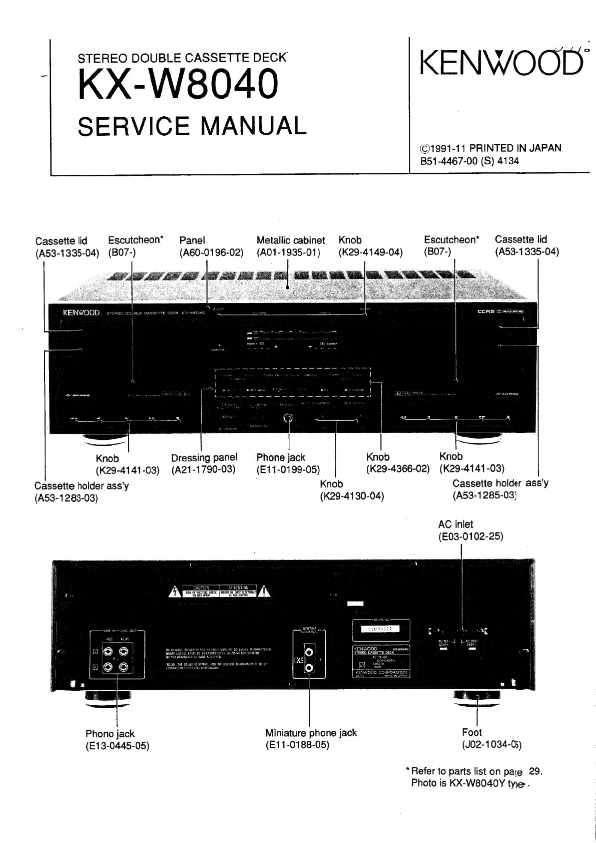
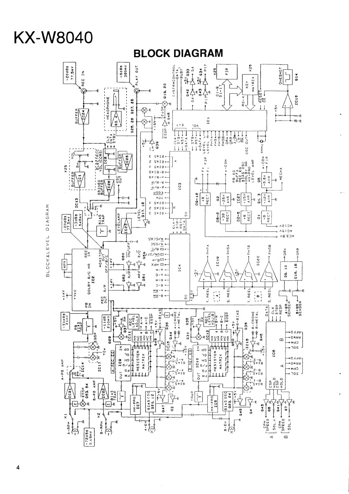
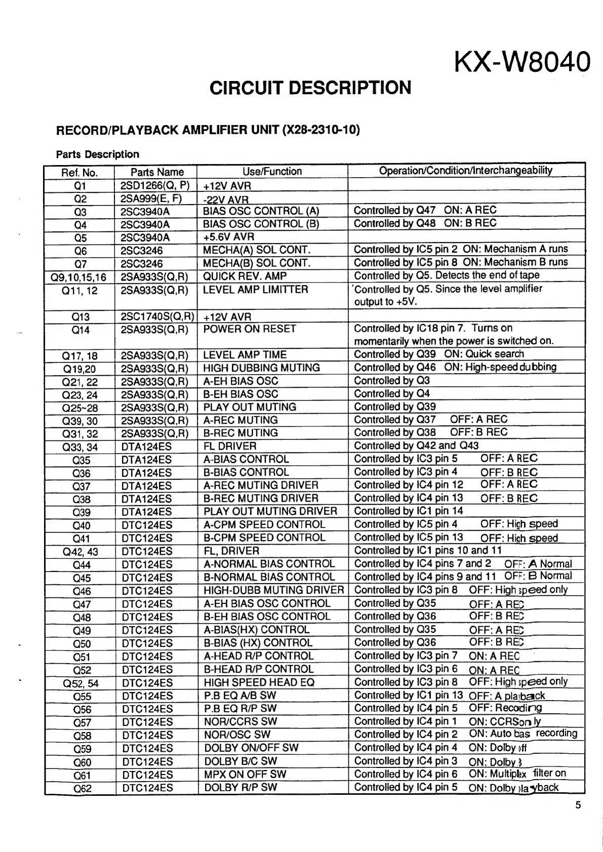
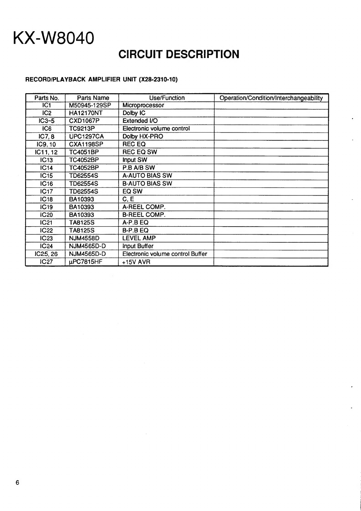
Kenwood KX-W8040 User manual

KX-W8040
lila
SERVICE
MANUAL
(1991-11
PRINTED
IN
JAPAN
B51-4467-00
(S)
4134
Cassette
lid
Escutcheon*
Panel
Metallic
cabinet
Knob
Escutcheon*
Cassette
lid
(A53-1335-04)
(BO7-)
(A60-0196-02)
(A01-1935-01)
(K29-4149-04)
(BO7-)
(A53-1335-04)
KENWOOD
ce
Knob
Dressing
pane!
=
Phone
jack
Knob
Knob
(K29-4141-03)
(A21-1790-03)
—§
(E11-0199-05)
(K29-4366-02)
(K29-4141-03)
Cassette
holder
ass'y
Knob
Cassette
holder
ass'y
(A53-1283-03)
(K29-4130-04)
(A53-1285-03)
AC
inlet
(E03-0102-25)
CAUTION
t
ATTENTION
RISK
OF
SLECTIMG
SHICK
{WSOC
DE
CHOC
ELECTRMUE|
DU
_NDT
OPEN
Ni
PAS
JUVE
Phono
jack
Miniature
phone
jack
Foot
(E13-0445-05)
(E11-0188-05)
(J02-1034-05)
“Refer
to
parts
list
on
pate
29.
Photo
is
KX-W8040Y
type.

KX-W8040
CONTENTS
DISASSEMBLY
FOR
REPAIR
..........ccseecesseeeeereeees
3
PC
BOARD
sisesstcstensas
Degiltranapehesa
ise
atop
enetbesmetaasiuaee
19
BLOCK
DIAGRAM
sivisatcscvencsivesesesecnnsiteitncnsstyatuvacsues
4
SCHEMATIC
DIAGRAM
.........ccesssesesesssseeesseeeseees
21
CIRGUIE
DESCRIP
TION
wccscnssoceietnasccaeusctentens
rane
5
EXPLODED
VIEW
(MECHANISM)
..........
cee
27
ADJUSTMENT
..0..ccecccceeesssestssscsesseneesssreneesseees
14
EXPLODED
VIEW
(UNIT)
covcicsecctiticcs
Giteaartveee
28
REGLAGE
soseicccsis
he
Steak
ca
lenteissiticsealvnsersssvacetoeannescie
15
PART
IST
ssitctiacircn
eciseaxguibenanniseataleniiess
29
ABGLEICH
vases
prsteretuiscinuscieccepocvanetvopnsaveceatsaesreenbetuas
16
SPECIFICATIONS.
ccccsccesecuavatessanecense
BACK
COVER
WIRING
DIAGRAM
siissiscossincieversisedesctisssstsotnedantans
18
Accessories
Audio
cord......
pe
(E30-0505-05)
Instruction
manual
B60-0777-00
(English)
System
control
cord......
1
B60-0778-00
(French)
P,E
(E30-
1392-05)
B60-0779-00
(Chinese)
M
B60-0780-00
(GE,
Du,
It)
E
AG
COM
as
cco
inacj
045956
1
B60-0830-00
(Spanish)
M
(Except
for
some
areas.)
(The
shape
may
vary
de-
pending
on
the
destination
Item
carton
case
area.)
(E30-1305-15:Y)
H50-0271-04
ae
Prine
itil
;
Polystyren
formd
fixture
(Except
for
some
areas.)
FQ
H10-5101-12
For
the
unit
with
a
Europe-
ca
an
AC
plug
in
areas
other
oe
H10-5102-12
than
Europe.
(E03-01
15-05)

KX-W8040
DISASSEMBLY
FOR
REPAIR
1.
How
to
remove
the
front
panel
@
Press
the
EJECT
button
to
open
the
cassette
holder
then
remove
the
cassette
lid.
Two
claws
of
escutcheon
pulling
out
side
then
remove
the
escutcheon.
(same
of
both
deck)
@
Remove
the
four
screws
of
bottom
(@)
2.
How
to
remove
the
mechanism
@®
Remove
the
four
screws
(@)
fxring
the
mechanism
assembly

KX-W8040
BLOCK
DIAGRAM
LOHSANO
ee
329
—
BE
we
PHWE
£3530
—
mea
PTs)
XIWIVW
dgWv¥
13A37
Sex
Otd-xH
Ag
wind
250
HN
AQTIO0<
>~Ou
I>
Wy
3s0_SvI9@
{ow
D3
330
vane
pes
03
aa
k—
Gud
dla
h—
7HO
woo-«
aSHd
Paine
vSHad
eV
LHG
FOI
4
43A30
-43
=
a
q3gaan
94,
vivo>
+
s[leise
=>
v9 vo
<4
ek
ee
=
EEO
et
2rd
vivo
asna
ase
viv
~|bLsais
—
:
ear
WOMINOIWELS4S
;
oro
oz
‘BtO
ino
Awd
a
AWOBE
SaP9~-
NI
O38
>)
y355N9
AWS
LE
SEp0e-
ay
-dS03
dSn3
-4-AGT
+
7
>
a
AG+
7
VHI3W
it
BHO)
at
“sto
Aztov
ASTOV
dl4
wON
woo-a
LAGS?
BlHd
ce)
m
oc
€
svig
e
$vIg
ao
AB
EDV
a
@
a
|
VSHd
+<
=
nae
=
XIW1VH
fF
usisisau
7
1938]
Vid
e+
ar~ea
a
|
vores
|
m
now
zlz
i
a
zlzl8
8
yYle
bP
bP
eo8g
UD
nnw
an
ay
s
~
“Mw
a
&
2
3x
°
H3-Vv
et
‘cto
soo
=
XIb1VvH
3
VAAAN
{
a
HBLSIS3aY
[|
——
440
/NO
d/d
LPS.
og
z@o
dWv13A3a7
Avi+
AVE
+
3787340
n
dvui|
f
ino
avs
3
Le
syra
ANWOLINOW
ot
zor
oe
1
uN
3/8
AB100
NI
ae
|
@d
AWBYS
Evol
|
sapc-
DOA+
AUS
CL
Pease
s@po2-
[
xan
|
Ape+
WVH9OVIGO
TSAAATRHIONG

KX-W8040
CIRCUIT
DESCRIPTION
RECORD/PLAYBACK
AMPLIFIER
UNIT
(X28-2310-10)
Parts
Description
[Qi
28D1266(Q,
P)
|
+12V
AVR
eee
|
G2
|
2SA999(E,
F)
|
-22V
AVR
ae
sake
See
eee!
25C3940A
IAS
OSC
CONTROL
(A)
|
4
28C3940A__|
BIAS
OSC
CONTROL
(B)
fea,
<<
(OGh
|
6
C
:
i
C
i
Use/Function
Operation/Condition/interchangeability
RS
ae
ee
eee
eee
ECHA(A)
SOL
CONT.
ECHA(B)
SOL
CONT.
UICK
REV.
AMP
Q11,
12
2SA933S(Q,R)
EVEL
AMP
LIMITTER
‘Controlled
by
Q5.
Since
the
level
amplifier
output
to
+5V.
ao
<
> <
Be)
[7
POs
2SC1740S(Q,R)[
+12VAVR
momentarily
when
the
power
is
switched
on.
|
Q25~28
|
2SA933S(Q,R)
[PLAYOUTMUTING
|
ControlledbyQ39
ontrolled
by
Q38_
OFF:
B
REC
FL
DRIVER
ontrolled
by
Q42
and
Q43
ontrolled
by
IC3
pin
5
OFF:
A
REC
ontrolled
by
IC3
pin
4
OFF:
B
REC
ontrolled
by
1C4
pin12
OFF:
AREC
ontrolled
by
IC4
pini3
OFF:BREC
ontrolled
by
IC1
pin
14
ontrolled
by
IC5
pin
4
OFF:
High
speed
ontrolled
by
IC5
pin
i3
OFF:
Hich
speed
ontrolled
by
IC1
pins
10
and
11
ontrolled
by
IC4
pins
7
and2
OFF:
A
Normal
A-BIAS
CONTROL
-BIAS
CONTROL
-REC
MUTING
DRIVER
-REC
MUTING
DRIVER
LAY
OUT
MUTING
DRIVER
|
Q40.—S«
|
DTC124ES
_—|
A-CPM
SPEED
CONTROL
B-CPM
SPEED
CONTROL
FL,
DRIVER
DTC124ES
-NORMAL
BIAS
CONTROL
DTC124ES
-NORMAL
BIAS
CONTROL
ontrolled
by
IC4
pins
9
and
11
OFF:
B
Normal
C
C
C
C
C
C
C
C
C.
C.
C
C
IGH-DUBB
MUTING
DRIVER
|
Controlled
by
IC3
pin8
OFF:
High
speed
onl
-EH
BIAS
OSC
CONTROL
__|
Controlled
by
Q35
OFF:
A
REC
-EH
BIAS
OSC
CONTROL
_|
Controlled
by
Q36
OFF:
B
REC
-BIAS(HX)
CONTROL
Controlled
by
Q35
OFF:
A
RES
-BIAS
(HX)
CONTROL
Controlled
by
Q36
OFF:
B
REC
-HEAD
R/P
CONTROL
Controlled
by
IC3
pin7
ON:
A
REC
-HEAD
R/P
CONTROL
Controlled
by
IC3
pin6
ON:
A
REC
IGH
SPEED
HEAD
EQ
Controlled
by
IC3
pin8
OFF:
High
speed
only
-BEQA/B
SW
Controlled
by
IC1
pin
13
OFF:
A
plaibaack
Ci
C
C
C
C
C
ontrolled
by
IC4
pin5
OFF:
Recodimg
ontrolled
by
1C4
pin1
ON:CCRSon!
ontrolled
by
IC4
pin
2
ON:
Auto
bas
recording
ontrolled
by
IC4
pin4
ON:
Dolby
off
ontrolled
by
IC4
pin3
ON:
Dolby
3
ontrolled
by
IC4
pin6
ON:
Multipbx
filter
on
Controlled
by
IC4
pin5
ON:
Dolby
jlayback
|
56
|
DTCI24ES
|
P-BEQR/P
SW
|
57S
|
DTC124ES
|
NOR/CCRS
SW
|
asa
|
DTC124ES__
|
NOR/OSC
SW
[ass
|
DTC124ES__|
DOLBY
ON/OFF
SW
Fa60
[|
DTC124ES_|
DOLBY
B/C
SW
PX
ON
OFF
SW
OLBY
R/P
SW

KX-W8040
CIRCUIT
DESCRIPTION
RECORD/PLAYBACK
AMPLIFIER
UNIT
(X28-2310-10)
Use/Function
Operation/Condition/Interchangeability
M50945-129SP
Eee
ie
Peg
ee
|
IC3~5
|
CxD1067P_——
|
Extended
VO
|
|
C6
|
TC9213P_|
Electronic
volume
control
=
|
|
1C7,8
[|
UPC1297CA
|
DolbyHX-PROU
|
|
ic9,10_
|
CxAiigssP_
|
RECEQ)
ee
ee
Pena
a
Ne
os
a
ara
e!
i
eee
ae
Pe
ene
ee
|
BA10393_—
ee
eae
ed
A-REEL
COMP.
fg
te
ge
el
BA10303____|
B-REELCOMP._—=—Ssd|—SSSSCSCSCSCSCSSCC~*r
Piozi_
[tastes
——SC«dARPBEQSSCSC~dSC“‘SWOCOC~“‘“*
[icx2
[tastes
_—-[BPBEQ
SSCs
SSSSCSCSCSSCC*r
ne
arena
Se
Sa
aad
Pr
ee
eee
ee

KX-W8040
CIRCUIT
DESCRIPTION
Micro
processor
(M50945-129SP)
Vref
O-
1
Vcc
LEVEL
L
©
2
AVcc
a
R
Oo
3
P1
PHTA
4
es
PHSA
5
P3
PHTB
O
6
P4
PHSB
O
7
PS
QRA
oO
8
P6
QRB
©
P7
P17
P8
G4
On
P9
KR4
P10
A
P11
LM
P12
V
CLK
O<
P13
V
DATA
c
P14
V
STB
¢
P15
EX
RST
P16
EX
CLK
cl
G1
EX
DATA
0«————
G2
EX
STB
Ox
G3
CE
G5
OSC
OUT
©
Gé
S
BUSY
©
G7
S
DATA
O<
G8
NC
G9
RESET
Vp
Xin
O———
KRO
Xout
oO
KR1
NC
KR2
NC
KR3
Vss
NC

KX-W8040
CIRCUIT
DESCRIPTION
Pin
Description
Name
LEVEL
L
LEVEL
R
PHTA
PHSA
PHTB
M
M
M
PinNo.}|
I/O
A/B
switching
output
_H:
B
deck
L:
A
deck
Line
mute
output
H:
MUTE
OFF
L:
MUTE
ON
_
=
ant
|
f
\X|
DIM
O|0
<
ala
SP
lass
:
ive]
ma
CLK
Extended
IC
clock
output
—ss—SSCSC‘“~*“‘~*~‘“‘~*~*~*~*~S~*S
Extended
IC
data
output
__—S—SC~—~—“—S~—SsSC‘“—SsSCSSS
Extended
IC
strobe
output
SSS
PAC
off
detection
H:ACON
LACOFFSSOS~—~SCS
[
400-Hz/10-kHz
output
forautobias——SSCSC—C~—~S~—~S~SY
'
Serial
busy
inputoutpat——SSSSSSSCSCSCS~—S
Serial
data
inpuvoutput_____—SSSSSSCSCSCS—CS—S
Connect
to
ground
———SSSSSCSC—~—SCSSY
nN
PO]
PO}
PO
a/fajoa}/oa}/ojoa}aol{a]oajou
=
O
iw)
O)NO,
OOM
Mmm
<<<
OW}
|
M|]
><]
><]
O<]
O<|
MD]
OO
S519)
(aigeiar
|
>|<
Sala
<
na 7)
XCIN
Connect
to
GND.
Pin
for
clock
pulses
for
time
display
COUT
OPEN.
_
Pin
for
clock
pulses
for
time
display
PG@oundpin
SY
ROPENS
ot
po
ee
Key
input
_FEKEVON
L:KEYORFE
"Key
input
H:
KEY
ON
L:KEVOFF
SSCS
wo
Key
input
H:
KEY
ON
L:
KEY
OFF
Key
input
H:
KEY
ON
L:
KEY
OFF
Connect
to
-30
V
High-voltage-resistant
port
pulldown
voltage
input
w
W]
Wd]
Ww]
ca
WIN]
MIN
w
(00)
wo
DOI
ODIQ
OOOO)
<j
AAA]
A]
Zl <|
x
09]
63]
G1]
|
NI]
Co]
MBBS
1
Dd
Banal
Be
ced
Bd
Pood
Rael
bd bo

KX-W8040
CIRCUIT
DESCRIPTION
Pin
Description
eee
a
ee
UNO
eS
er
Fluorescent
segment
output
n
Fluorescent
segment
output
o
luorescent
segment
output
p
Analog-to-digital
converter
power
supply.
Connect
to
backed-up
+5V.
Power
supply
pin.
Connect
to
backed-up
+5V.
O
-
™N
rir
oO
ie)
ain
=
COIN
fo?)
°
=
=
Ot
hel
>
<
S$
ro)
<
cc

KX-W8040
CIRCUIT
DESCRIPTION
/O
EXPANDER
(CXD1067P)
1/0
1
A
BIAS3
1
YDD
A
BIAS2
2
CLK
A
BIAS]
3
DATA
B
BIAS
4
-
STB
A
BIAS
5
RESET
B
R/P
6
SET
A
R/P
7
50
EQSP
8
Pl2
B
BIAS3
70u
9
Pll
B
BIAS2
1
P10
B
BIAS1
1/0
2
CCRS/NOR
1
VDD
OSC/NOR
2
CLK
DOLBY
B/C
3
DATA
DOLBY
ON/OFF
4
STB
DOLBY
R/P
5
RESET
MPX
6
SET
A
METAL
7
SO
A
Cr02
8
P12
B
RECMUTE
B
METAL
9
Pid
A
RECMUTE
1
P10
B
Cr02
be
x3
A
SOL
1
A
HOLD
2
A
CPK
3
A
CSP
4
A
RRW
K)
A
REF
6
B SOL
7
B
HOLD
8
B
CSP
B CPH 9
B
RRW
1
B
REF
10

KX-W8040
CIRCUIT
DESCRIPTION
Pin
Description
VO
1.
PWON=
=
Nate.
_
[a
PUCHOR
[|
O
[ABIAS3
|
ForAUTOBIAS
fordeckA
PO
[ABIAS2
[For
AUTOBIAS
fordeckA
|
O
[ABIAS!
[|
For
AUTOBIAS
fordeckA
|
O
|
BBIAS
[|
Bbiascontrol
CH:
BIASON
L:BIASOFF
|
O
[ABIAS
[Abiascontrol
CH
BIASON
L:BIASOFF
|
oO
[BRP
|
BREC/PLAY
switching
CH:
REC
L:PLAY
|
Pin
No.
|
pee
fete
es
eee
|
5
eam
B
i
a
B
a
AON
zi
7
[|
0
|
i
8
|
O
|
EQSP
|
Brecord
equalization
switching
_H:
NORMAL
SPEED
__L:
HIGH
SPEED|
[Oo
[7
__|
Playback
equalization
time-constant
switching
_H:7ous L:120us
|
P=
[Vss_———s|
Connecttoground.
11
|
O
|
BBIAS1
|
ForAUTOBIASfordeckB
[42
[
O
|
BBIAS2
|
ForAUTOBIASfordeckB
[13
|
O
[BBIASS
|
ForAUTOBIASfordeckB
|
14
{|
O
[SO
|
Dataoutputpin.
Connecttothedatapinof
VO
expander2.
[is
[1
[SET
sé:
Connectto
VDD
(+5V).
H:
NORMAL
L:AllportsarelowH
|
:
ee
H:
NORMAL
_L:
All
ports
are
low
L
T1417
|
1
[STB
___|
Strobe
signal
input
in.
Connect
to
the
EXST
pin
of
the
microprocessor.
[ig
|
1
|
DATA
__|
Datainputpin.
Connect
tothe
EXDATApin
of
the
microprocesso.__|
[19
|
|
[CuK
|
Clockinputpin.
Connectto
the
EXCLK
pin
of
the
microprocessor.
[20
[
-
|
~~
__|
Powersupplypin.
Connectto+5V.
02.
[WO]
Name
[SSCSC~SCSCSCCCSC*S
CHM
SCSC—=*
ASOL
A
solenoid
control
H:
ON
_L:
OFF
AHOLD
solenoid
hold
control
H:ON
L:
OFF
A
A
main
motor
control.
Hub
motor
speed
change.
H:ON
__L:
OFF
A
A
|ACSP._—_—s{
Amain
motor
speed
change
=H:
NORMAL
SPEED
_L:
HIGH
SPEED
PARRW_|
Areel
motor
control
_—_—H:
REWIND,
RVS
__L:
Others
[ARFF
[BSOL_
A
i
;
A
i
:
A
: :
A
A
reel
motor
control
H:
FF,
FWD
L:
Others
B
SOL
B
solenoid
control
H:ON
L:
OFF
B
i
:
B
mai
; :
B
S}
S}
B
HOLD
solenoid
hold
control
H:
ON
L:
OFF
BCPM
main
motor
control.
Reel
motor
speed
change.
H:O0N
LL:
O[F
0
Ground
pin.
Connect
to
ground.
|
O
|
|
Oo
|
|
O
|
|
O
|
|
O
|
p20)
|
O
|
|
O
|
EOS]
see
|
O
|BRFF
|
Breel
motor
control
SH
FF,FWD
iL:
Others
|
O
|
B
|
O
|
|
O
|
=
ie
Ee
te
oz
BCSP
B
main
motor
speed
change
H:
NORMAL
_
L:
HIGH
SPEED
1SO.-—_{
Data
output
pin.
OPEN
FINO,
es
a
hee
Eso
esa
ee
Kare
ee
ieee
1
1
1
1
SET
|
Connect
io
VOD
(«5V).
Hi:
NORMAL
_L:
Allporis
are
low
4
7
1
|
20
|
CSP
RRW
RFF
reel
motor
control
H:
REWIND,
RVS
_L:
Others
O
ET
:
RESET
Connect
to
the
EXRST
pin
of
the
microprocessor.
H:
NORMAL
__L:
All
ports
are
low
Stobe
signal
input
pin.
Connect
to
the
EXST
pin
of
the
microprocessor.
DATA
Data
input
pin.
Connect
to
the
SO
pin
of
I/O
expander
2
Clock
input
pin.
Connect
to
the
EXCLK
pin
of
the
microprocessor
Power
supply
pin.
Connect
to
+5V.
11

KX-W8040
12
CIRCUIT
DESCRIPTION
V0
3.
Pin.
Now)
|
WOS))
2
Names
Use
et
PUNTO
ea
|
1
|
0
|
CCRSWNOR
|
CCRS/normal
switching
HH:
CCRS__L:
NORMAL
__
|
2
OSC/NOR
AUTOBIAS/normal
switching
H:
AUTOBIAS
L:
NORMAL
DOLBY
B/C
Dolby
B/C
switching
H:
B
TYPE
L:
C
TYPE
Dolby
REC/PLAY
switching
H:
PLAY
L:
REC
Tr
6
MPX
on/off
control
H:
MPX
ON
L:
MPX
OFF
|
8
[|
|
A
recording
equalization
switching
|
9
|
A
RECMUTE
A
recording
mute
control
H:
REC
MUTE
OFF
_L:
REC
MUTE
ON
B
RECMUTE
B
recording
mute
control
H:
REC
MUTE
OFF
L:
REC
MUTE
ON
Data
output
pin.
Connect
to
the
data
pin
of
I/O
expander
3.
Connect
to
VDD
(+5V).
H:
NORMAL
L:
ALL
ports
are
low
Connect
to
the
EXRST
pin
of
the
microprocessor.
H:
NORMAL
L:
ALL
ports
are
low
Clock
input
pin.
Connect
to
the
EXCLK
pin
of
the
microprocessor
Power
supply
pin.
Connect
to
+5V.
|
O
|
20%)
Ore
Ors
|
O
Oe
om
|_
O
|
=
P
ii
[|
O
|
|
Brrecording
equalization
switching
H:CrO2__L:
NOT
METAL
__
|
|
O
|
|
O
|
Oo
ale
ee
ie
ee
ae!

KX-W8040
CIRCUIT
DESCRIPTION
Test
Mode
(b)
Cancel
1.
Test
1
To
cancel
the
test
mode,
press
the
PAUSE
key
(a)
Setting
on
deck
A
or
B,
or
switch
the
power
off.
Note
Short
test
pins
(TP 3
4-4)
with
a
diode,
and
plug
that
the
direction
and
counter
values
while
in
the
in
the
AC
cord.
test
mode
are
stored
in
memory.
If
the
AC
cord
is
disconnected
while
in
the
test
mode,
the
memory
is
initialized
completely.
All
indicators
light
two
seconds
after
the
power
is
switched
on,
then
the
normal
display
resumes
(except
for
the
meter
section).
(c)
Operation
All
indicators
on
L
INHFA
CrO2A
METALA_
INHRA
-15
-10
6
3
on
ae)
(oe)
R
INHFB
CrO2B
METALB_
INHRB
Mechanical
switch
display
(DIRECTION
switch)
When
the
REC
key
is
pressed,
the
counter
is
reset
to
0.000,
recording
is
done
forfour
seconds,
then
the
recorded
part
is
played
back
from
the
beginning.
*
The
key
is
accepted
at
any
time.
Four-second
recording
(for
decks
A
and
B)
Deck
A
high-speed
playback
4
seconds
Timer
play
Deck
A
normal-speed
playback
12
seconds
Deck
B
high-speed
playback
4
seconds
Deck
B
normal-speed
playback
12
seconds
Deck
B
recording
15
seconds
Rewind
to
the
beginning.
Time
recording
Deck
B
playback
13
seconds
Deck
B
stop
Note:
Time
recording
is
not
done
if
there
is
no
cassette
in
deck
B.
FWD
PLAY
key
------+-+-
Normal
playback
(FWD)
FF
key
sess
esene
High-speed
playback
(FWD)
Speed
change
RVS
PLAY
key
«+--+
Normal
playback
(RVS)
RWD
key
ecevennes
Rewind
Note:
If
the
FWD
PLAY
and
FF
keys
are
pressed
altermately,
the
head
dones
notretract.
When
the
H.
CCRS
key
is
pressed,
high-speed
recording
is
done
on
deck
B.
High-speed
recording
Note:
High-speed
recording
is
not
done
if
there
is
no
cassette
in
deck
B.
Dubbing
H
<«{$—>L
Input
level
ATT
Keys
to
be
inhibited
if
the
H.
DUB
and
N.
DUB
keys
are
pressed
alternately,
the
dubbing
speed
can
be
changed
without
retracting
the
head.
Note:
The
speed
cannot
be
changed
if
there
is
no
cassette
in
deck
B.
When
the
N.
CCRS
key
is
pressed,
recording
pauses,
and
the
level
can
be
input.
If
the
input
is
excessive
(+5
dB
or
higher),
the
PWM
is
changed
and
the
level
is
set.
Wen
the
B.
REC
key
is
pressed,
recording
can
be
done
at
the
specified
level.
Note
that
the
level
is
canceled
when
another
operation
is
performed.
The
DPSS
mode
is
not
entered.
Note
that
the
display
is
slightly
different
from
them
ormal
one.
13

KX-W8040
14
INPUT
OUTPUT
CASSETTE
TAPE
ALIGNMENT
ITEM
SETTINGS
SETTINGS
DECK
SETTINGS
POINTS
ALIGN
FOR
CASSETTE
DECK
SECTION
TAPE:
NORMAL,
DOLBY:
OFF,
INPUT:
LINE
OdBs
=0.775V
1
REC/PLAY
HEAD
POWER:
OFF
Demagnetize
the
REC/PLAY
C1)
|
DEMAGNETIZATION
Remove
the
REC/PLAY
head with
a
head
cassette
door.
head
demagnetizer.
REC/PLAY
Clean
the
REC/PLAY
head
head
erase
head,
capstan
and
CLEANING
erase
head,
Pinch
roller
using
a
cotto
capstan,
swab
slightly
daaped
pinch
roller.
with
alcohol.
MTT-114,
TCC-153
Azimuth
SCC-1727
10kHz,
-10dB
AZIMUTH
adjustment
screw
Maximum
output.
1
PC
BOARD
(X28-—231)
Adjust
the
tape
speed
so
MTT-111,
TCC-110
DECK
A:
;
:
TAPE
SPEED
SCC-1727
DECK
B:
that
a
6kHz
signal
is
(HL
SPEED)
3kHz
Test
mode
test
YR1
(VR103)
on
each
Produced
at
the
center
-4dB
FF
key
HI
speed
own
mechanism
board
of
the
tape,
F.
PLAY
key
;
MTT-111,
TCC-110
Normal
speed
|
DECK
A:
Adjust
the
tape
speed
so
TAPE
SPEED
SCC-1727
DECK
B:
that
a
3kHz
signal
is
CRORMAL)
3kHz
VR2
(VR223)
on
each
produced
at
the
center
-4dB
own
mechanism
board
of
the
tape.
Connect
a
DC
DECK
A:
VR9
Adjust
the
semi-fixed
voltmeter
to
DECK
B:
VR10
resistanceso
that
TPS
and
GND
(A)
TP6
and
GND
(B)
ene
Output
level:
-3.0dBs
Use
the
leader
section
of
the
test
tape.
MTT-150
400H2(200n¥b)
QUICK
REVERSE
SENSITIVITY
M
PC
BOARD
(X28-231
)
DECK
A:VRIL)
2-3,
PLAYBACK
MTT-256,
SCC-1727
VRAR)
<I>
LEVEL
315Hz
(160nWb)
(B)
PLAY
DECK
B:VRRXL)
NTT-256U,
TCC-160
VRARI
SCC-1176
Output
level:
-2.0dBs
315H2(220n¥b)
Adjust
REC
level
volume
so
that
the
REC
monitor
output
becomes
«29dBs
at
LkHz,
then
record
and
reproduce
signal
of
IkHz-and
10kHz
in
alaternation.
Record
IkHz
and
10kHz
in
alternation
and
adjust
the
variable
resistors
which
DECK
A:VRO(L)
VRGIR}
DECK
B:VR7{L)
VR8IR)
(A)
IkHz,
~30dBs
10kHz,
-30dBs
BIAS
CURRENT
control
the
bias
current
so
that
the
same
playback
level
is
obtained.
onnect
the
frequency
Load
the
counter
between
BIAS
OSCILLATING
non
recorded
TPL
and
GND
DECK
A:L3
Adjust
so
that
the
FREQUENCY
tapes
on
Deck
on
Deck
A,
between
DECK
BL
4
frequency
counter
A
and
B.
TP2
and
GND
shows
1LQ5kHz.
on
Deck
B.
Load
a
Load
a
aetal
tape,
DECK
A:L5(L)
<4
BIAS
LEAK
non
recorded
and
dub
in
a
ue
Mininua
(Point)
DECK
B:L7(L)
tape
on
Deck
A
high
speed
mode.
L8(R)

KX-W8040
REGLAGE
REGLAGE
DE
REGLAGE
DE
REGLAGE
DU
MAGNETO
POIKTS
DE
nN"
ITEM
L’
ENTREE
LA
SORTIE
~PHONE
A
CASSETTE
L’
ALIGNEMENT
ALIGNER
POUR
FIG.
SECTION
DU
MACNETOPHONE
TAPE:
NORMAL,
DOLBY:
OFF.
EXTREE:
LINE
OdBs
=
0,775V
{
TETE
D’
ENRECISTREMENT/LECTURE
Demagnétiser
la
téte
POWER:
OFF
Tate
D’
ENREGISTREMENT/LECTURE
DEMAGNETISATION
Eloigner
!a
porte.|
D’
ENREGISTREMENT/
avec
un
démagnétiseur
LECTURE
de
téte.
Téle
Nettoyer
ta
téte
D'
EXREGISTREMENT/
D’
ENREGISTREMENT/LECTURE
LECTURE
téle
la
tete
d
effacement,
le
NETTOYAGE
-
d
effacement,
pabeeten
et
le
galetpresseu
cabestan,
avec
un
coton-tige
—t
galetpresscur.
légérement
imbibé
d'
alcool.
MTT-114,
TCC-153
AZAMUT
SCC-1727
Vis
d’
azimut
Sortie
maximer.
(a)
10kHz,
-10dB
PLAQUE
IKPRIMEE
(X28-231)
MTT-111,
TCC-110
DECK
A:
Réegler
la
vitesse
de
banda
VITESSE
DE
SCC-1727
DECK
B:
de
facon
qu'un
signal
C1
)|
DEFILEMENT
3kHz
VR1
(VR103)
sur
chaque
|
de
6kHz
soit
produit
au
(HI.
SPEED)
~4dB
H
igacetaey
Plegetie:de
mrcev
ars
centre
de
la
bande.
MTT-111,
TCC-110
F.
PLAY:Normal
speed
|
DECK
A:
Realer
la
vitesse
de
bande
VITESSE
DE
SCC-1727
DECK
B:
de
facon
qu'un
signa!
(2)|
DEFILEKENT
3kHz
VR2
(VR223)
sur
chaque
|
de
3kiiz
soit
produil
au
(NORMAL)
-4dB
Plaquette
de
mécanisme
centre
de
la
bande.
SERSIBILITE
Utiliser
ees
DECK
A:
VR9
Ajuster
ta
résistance
(3){
D'
IRVERSIOX
la
sect
ion-guide
ee
END)
DECK
B:
VR10
semi-fixe
pour
que
(b)
RAPIDE
de
la
bande
test
4
TP6
et
GND
(B)
la
tension
0,75¥(40,15Y)
soit
obtenue.
TM
PLAQUE
IMPRIMEE
(X
28-231
MTT-150
400HZ2(200n¥b)
MTT-256,
SCC-1727
315Hz
(160nWb)
WTT-256U.
TCC-160
SCC-1176
315Hz(220n¥b)
DECK
A:VRUGI
Niveau
de
sortie:
-3.0iBs
VRAD
DECK
B:
VR3GI
VRAD)
NIVEAU
DE
LECTURE
Niveau
de
sortie:
-6.01Bs
Niveau
de
sortie:
-2.01Bs
Régter
REC
de
volume
de
niveau
facon
que
la
Enregistrer
un
sigmi
de
sortie
de
moniteur
DECK
A:
VR5IG)
IkHz
et
-LOkH2
en
alternance
COURAXT
DE
(A)
REC
soit
de
-29dBs
VR¢@(D)
el
ajuster
les
résislances
€2>]
POLARISATION
ikHz.
-30dBs
(B)
a
lkHz,
puis
en
DECK
B:
VRUG)
variables
qui
commadent
10kHz.
-30dBs
VR8(D}
le
courant
de
polarilé
de
facon
a
obtenir
le
néme
niveau
de
lecture.
eee
ew
registrer
et
reproduire
des
signaux
de
[kHz
et
10kiz
en
alternance.
Raccorder
le
FREQUENCE
Wettre
en
place
|
compteur
de
frequenca
D’
OSCILLATION
des
cassettes
enter
TPl
et
GXD
de
DECK
A‘1.
3
Regler
de
sanice
€3>
|
DE
POLARISATION
|
non
enregistrees
|
Ja
platine
A,
enter
|
Enregistrement
DECK
B:L
4
ace
que
le
computer
de
|
(c)
dans
les
platines
TP2
et
GND
de
ta
(X28
-1380-01)
frequence
indique
ISkHz.
A
et
B.
Wettre
en
place
platine
B.
Mettre
en
place
PUITE
DE
une
cassette
non
unebande
metal
et
aaa
<4>
|
POLARISATION
|
enregistree
dans
(B)
copier
en
mode
de
DECK
B:L7(G)
Wininum
(point
L8(D)
Ja
platine
A
vitesse
elevee.
15

KX-W8040
ABGLEICH
CASSETTEN-DECK-ABTEILUNG
TAPE:
NORMAL,
DOLBY:
OFF,
EINGANG:
LINE
OdBs
=0.775¥
1
AUPNAHME/W1EDERGABE
KOPR
POWER:
OFF
Den
Kassettenfach
Entmagnetisierung
von
dem
AUFNAHWE/WI
EDERGABE-Kopf
ait
einem
Tonkopf
Entmagnetisierungsdrossel,
AUF
NAHME/¥{
EDERGABE-Kopf,
AUPNAHWE/
WIEDERGABE-Kopf
ENTMAGNETI
-
{1]
STERUNG
deckel
oben
herausziehen.
AUFNAHWE/
WIEDERGABE-Kopf
Loschkopf,
Tonwelle
und
{2]
REINIGUNG
PLAY
Loschkopf,
Andruckrolle
mit
einem
Tonwelle,
leicht
mit
Alkohol
befeuch
Andruckrolle.
teten
Wattebausch
reinigen.
Azimut-
Einstel!schraube
AZIMUT
MTT-114,
TCC-153
{3]]
EINSTELLUNG
SCC-1727
(B)
PLAY
10kHz,
-10dB
|
GEDRUCKTE
SCHALTPLATTE
(X
28-231
)
Maximal
Ausgang.
(a)
Einen
Schaltdraht
DECK
A:
BANDGESCH-
at
zwischen
DECK
B.
Die
Bandgeschwindigkeit
WINDIGKEIT
pede
(B)
GND
und
TP3
VR1
(VR103)
anf
der
so
justieren,
da@
ein
(HI
SPEED)
“A6B
anschlieBen.
jeweils
eigenen
6kHz
Signal
auf
der
Mitte
Mechanismus-Pldtine
PLAY
des
Bands
erzeugt
wird.
MTT-111,
TCC-110
ee
5
Die
Bandgeschwindigkeit
BANDGESCH~-
SCC-1727
:
so
justieren,
daB
ein
Ent
VR2
(VR223)
anf
der
:
:
(2)
VINDIGKEIT
3kHz
jewells
eigenen
3kHz
Signal
auf
der
Mitte
-44B
des
Bands
erzeugt
wird.
Den
halbfesten
Viederstand
so
einstellen,
da.
die
Spannung
0,75V
(10,15V)
betragt.
Pidtin
Mechanismus-
e
Eine
Gleichspannungs-
messer
an
TPS
und
GND
(A),
TP6
und
GND
(B)
anschliefen.
DECK
A:
VR9
DECK
B:
VR10
(NORMAL)
A
SCHNELLRUCKLAUF
-
Den
VYorspann
(3.)|
EMPFINDLICHKEIT
|
des
Testbandes
versenden.
I
GEDRUCKTE
SCHALTPLATTE
(X
28-231
)
MIT-150
40082
(200n¥b)
DECK
A:VRIIL}
WIEDERGABE-
|
MTT-256,
SCC-1727
A
VRQR)
eer
ae
315Hz
(160nWb)
DECK
B:
VR3(L)
Ausgangspegel:
-6.0dBs
MTT-256U,
TCC-160
VRAR)
SCC-1176
315H2(220n¥b)
Ausgangspegel:
-2.0dBs
REC
so
Pegel
Lautstarke
justieren,
da8 der
REC
Monitorausgang
-29dBs
bei
LkHz
wird,
und
danach
abwechselnd
Signal
von
ikHz
und
10kHz
aufnehmen
und
Signale
von
IkHz
und
10kHz
abwechselnd
aufnehmen
und
die
Regelwiderstande,
die
DECK
A:
VR(L)
5(L)
VRIR)
6(R)
DECK
B:VR(L)
7{(L)
VR(R)
8(R)
(A)
1kHz.-30dBs
10kHz.-30dBs
LEERLAUFSTROM
den
Vormagnetisierugsstrom
regeln,
so
justieren,
das
der
gleiche
Wiedergabepege]
erzielt
wird.
wiedergeben.
Den
Frequenzzahler
Unbespielte
zwischen
TPl
und
ORMAGNETISIERUNGQ
Kassetten
in
GND
von
Deck
A
DECK
A:L
3
So
einstellen,
de®
105kHz
OSZILLATIONS-
Deck
A
und
B
und
zwischen
TP2
DECK
B:L
4
auf
dem
Frequenzzahler
FREQUENZ
und
GND
von
Deck
B
anschlieGen.
einsetzen.
angezeigt
wird.
Eine
Metal
lband-
kassette
einsetzen
und
nit
hoher
Geschwindigkeit
Uberspielen.
DECK
A:LS(L)
L6(R)
DECK
B:L7(L)
La(R)
VORMAGNETISIE-
RUNGSSTREUUNG
Eine
unbespielte
kassette
in
Deck
A
einsetzen,
Minimum
(Punkt)
16

KX-W8040
KX-W8040
ADJUSTMENT/REGLAGE/ABGLEICH
WIRING
DIAGRAM
|
GNO]>
|
(¥/)
(-G2Xx)
|
Lote
(G0
-2SZO-201)
SdAL
W‘A)
(G0
-8G20-201)
AOEZOV
(AdAL
3'L'X)
TT
_
~~]
(SO
-9GZ0-201)
AOZIOV
(AdAL
d‘™)
||
ba
SANOHd
(a)
AZIMUTH
ADJUSTMENT
SCREW
KX-W8030
SYSTEM
CONNECTIONS
|
eee
d=
|
(v/9)
|
(-82x)
V
y
1
FORWARD
Frequency
counter
Frequencemetre
Frequenzzahler
eee
000
Ge
AC
voltmeter
Voltmetre
CA
Oscilloscope
Wechselspan-
Oscilloscope
nungsmesser
Oszilloskop
2
ae}
a
so
)
Soau
2026
w&
S555]
Jee!
oY
1
0205
oe}
eave
OO
Ou
Go
LOUEZZO
PAerafa
wea
S-Oga
2
Poune
a
63.
EzoP
fs
offa
SEGS
cools
a>3¢
<}ENO
LINN
AVidsia
(b/¥)
(Ol-OlEb-S2Xx)
iw
an
(¢0-8960-07a)
|
X'‘W‘A‘d
(¢0-9960-0ra)
|
a
ASSV
|
WSINVHOAW
:
(o/V)
(XX-OIE2-
82x)
LINN
MOVEAV
Id
/
GYHODaY
J
1
(S0-2960-07q)
1
X'W'A‘d
(S0-S960-0rq)
Vv
ASSV
WSINVHOAW
Apes
[oS
O}{S
O}+
{0
O}—
—
a
Y¥
7
TOYLNOD
ino
NI
OYDNAS
&
17

K
L
M
N
fe)
P
Q
R
s
;
T
PC
BOARD
(Component
side
view)
WH7
p-Raé7
C200"
SYSTEM
CONTROL
REC
LEVEL
REC
BALANCE
4
Out
X25
C/4,¢
AR”
:
Refer
to
the
schematic
diagram
for
the
values
of
resistors
and
capacitors.
19
20

WW
A
DECK
gpd
ee
ee
ee
a
fal
ed
ae
(2)
ba
ig
ipsa
meme
J-_t_{o|
—__to
NC
R.REC
HOLE
com}
Cro
F.REC
METAL
com2
Lich
>
R/P
HEAD
Reh
Sd
Nd
ERASE
HEAD
X
TA7291S
O.1V
(REC)
A-
DECK
BIAS
ERO
MOSK
Hz
}
B
DECK
ee
ee
a
res
one
oman}
re
a
2
R/P
HEAD
@
>:
ae
Roe
wo?
&
oO
@)
lo}
——_o
NC
R.REC
HALF
com!
croz
FLREC
METAL,
COM
2
ERASE
HEAD
4
TATZIIS
SPI-
320
SPI-
335-34
WE
0.1V
(REC)
|
I5v
(PLAY,
STOP)
REEL
S-V
REEL
V
M.REEL
‘M.REEL
KICK
CPM
GND
+8
sP
‘SOL
B-
DECK
Bias
EROY
OSKH2)
2sc4202
2SA999
2801845
2S8C3246
ISVUPLAY,STOP)
cia
I50P
250
2SD1266
25C3940A
€
Ic22t/2)
6.0V.
1222/2)
O7V
DTA124ES
DTC124ES
UN4112
2SA933S
2801740S
comp.
Y
PEAK
asso
LJ
ET
|
DET
a
STAOILIZING
POWER
SOURCE
REC
PLAY
REC.
HAVIN)
STOP
|
syiyy
LSViC)
OV
Faye)
Ma
3.5v(M)
56K.
BIAS
ON/OFF
c73
om
|
220P
us
UN4212
25A1309A
28C3311A
NJM4558D
REC
L3VIN)
Lgevicd
3.5viM)
REC
OvIND
4.2vic)
4.2v
iM)
oviN)
4.3vIc)
a7viny
—
33ViC)
PLAY,
STOP
ov
NJM4565D-D
5
8
‘
4
1
Bias
ON/OFF]
CXA1198AP
XRU4051B
XRU4052B
TC4051BP
TC4052BP
TC9213P
s+
BUSY
AN
BA1039¢
TA8215S
CXD1067P
Saye
TD62554S
w

cr?
Re
47
35
ik
+=
Le]
=
y
in
s
Q37
4
C75.
4
ig
“ue
7Q
RI39
Lev
C>
AM
rid
Ped
Paty Tet]
Le
eS
:
kK)
[ark
sem
cme
Ft
A
t
|
(ste_10)
‘
;
[INPUT
BUFFER]
fee
eta
ae
ET
Bh
“ed
ot
=
Me
.
‘
3
1c240172)
atest
ts
)
:
ye
rat
Tt
ttn
Pi
fat
fi
on
LLOVIOFFD
6.6vi8)
H.6VIC)
C76
4%y
35
47
35
R80
510
ae
Pe,
fe
Pe
an
Fg
gc
ag
eagu
ages
«
1
RP
LEVEL
AMP
IC23(272)
ia
R267
Mm
Wecrsd
C96
lop
35
a
K
D
>
D74
D072
prolae
—<4
ee
Sai
:
as
3
1c230v2)
100k 100P
RI74
C100
REC
oviNd
azvin)
—
4.3ViC)
Sea
ee
i
|
ovic)
7
|
|
&
+h
a
|
:
TT
“ill
R2i2
R208
|
[|
10K
=
100K
ti2v
[19
91
i)
2
3
(KP
TYPE)
OGTE
TF
(
X28-)
(
©
®
@®
®
@
©
Bias
‘ON/OFF
(YM
TYPE)
2
DC
voltages
are
as
measured
with
a
high
impedance
voltme-
Die
angegebenen
Gleichipannungswerte
wurd:
TC4051BP
TA8215S
CXD1067P
BA10393
UPC7815HF
HA12170NT
UPC1297CA
M50945-129SP
ter
with
a
cassette
loaded
at
playback
mode.
Values
may
vary
setzter
Cassette
in
der
Wiedergabe
mit
einem
|
TC4052BP
TD62554S
"
RC4565D-D
-
slightly
due
to
variations
between
individual
instruments
Spannungsmesser
gemessen.
Dabei
schwank
TC9213P
.
"
33
or/and
units.
Bias
circuit
DC
voltages
are
as
measured
while
in
werte
aufgrund
von
Unesschieden
zwischen
;
;
site
,
the
record
mode.
strumenten
oder
Gerdtenus.
U.
geringfiigig.
Die
rt
%
‘
32
‘ :
Fi
Gleichspannungswerte
der
Vormagnetisieru
°
GND
: :
64
Les
tensions
c.c.
doivent
étre
mesurées
avec
un
voltmétre
a
,
:
6
U
U
wwpuT
(Case)
Y
"
haute
impedance,
une
cassette
étant
inserée
en
mode
du
lec-
wrurdeniin
der
Autrishme-testriebeart
gemeasen.
8
8
20
1
: ‘
'
ture.
Les
valeurs
peuvent
differer
egerement
du
fait
des
varia-
1
tions
inhérentes
aux
appareils
et
aux
instruments
de
mesure
1
individuels.
Les
tensions
c.c.
du
circuit
de
polarité
doivent
étre
mesurées,
l'appareil
étant
en
mode
d’enregistrement.
Other manuals for KX-W8040
2
Other Kenwood Cassette Player manuals

Kenwood
Kenwood CP-J7 User manual

Kenwood
Kenwood X-E5 User manual

Kenwood
Kenwood KXF-W4030-S User manual

Kenwood
Kenwood KRC-940 User manual

Kenwood
Kenwood X-SE7 User manual

Kenwood
Kenwood KX-W8050 User manual

Kenwood
Kenwood KX-W8060 User manual

Kenwood
Kenwood CP-J7 User manual

Kenwood
Kenwood KX-830 User manual

Kenwood
Kenwood KRC-V791 User manual

Kenwood
Kenwood KRC-31 User manual

Kenwood
Kenwood KX-4520 User manual

Kenwood
Kenwood KX-W4050 User manual

Kenwood
Kenwood KDT-99R User manual

Kenwood
Kenwood KX-1030 User manual

Kenwood
Kenwood CT Series User manual

Kenwood
Kenwood CT-203 User manual

Kenwood
Kenwood KX-W6050 User manual

Kenwood
Kenwood X-S300 User manual

Kenwood
Kenwood CT-203 User manual