8
TK-5400
1. Overview
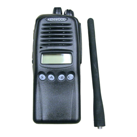
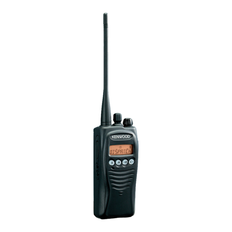
The KENWOOD model TK-5400 is an 800MHz/FM/APCO
hand-held transceiver designed to operate in the frequency
range of 806 to 825MHz (TX)., 851 to 870MHz (TX/RX), the
unit consists of a receiver, a transmitter, a phase-locked
loop (PLL) frequency synthesizer, base band parts, power
supply circuits, a control unit.
2. Circuit Configuration by Frequency
The receiver is a double-conversion superheterodyne us-
ing first intermediate frequency (IF) of 44.85MHz and sec-
ond IF of 455kHz. Incoming signals from the antenna are
mixed with the local signal from the PLL circuit to produce
the first IF of 44.85MHz.
This is then mixed with the 44.395MHz second local os-
cillator output to produce the 455kHz second IF. This signal
is detected to give the demodulated signal in the DSP.
The transmit signal frequency is generated by the PLL
VCO, and modulated by the signal from the DSP. It is then
amplified and fed to the antenna.
The VCO oscillation frequencies are 403 to 412.5MHz
and 425.5 to 435MHz, and locking occurs at both ranges of
doubled frequencies of 806 to 825MHz and 851 to 870MHz.
The VCO output components, other than the doubled fre-
quencies, are eliminated by a band-pass filter, and the re-
sulting signal is amplified by a buffer amplifier (Q201) and
routed to pin 5 of the PLL IC. The VCO output is amplified
by two buffer amplifiers (Q205, Q206) and routed to the
transmit drive stage and receiver mixer through the TX/RX
switch (D101, D102).
The PLL IC consists of a prescaler, a fractional divider, a
reference divider, phase a comparator and a charge pump.
The PLL IC is a fractional N type synthesizer and operates at
100kHz, which is 8 times the 12.5kHz channel step. The
input signal from pins 5 and 16 of the PLL IC are divided to
100kHz in the PLL IC and compared with a phase compara-
tor. The pulse output signal of the phase comparator is ap-
plied to the charge pump and converted to a DC signal with
a loop filter (LPF). The DC signal is applied to pin 4 of the
VCO and locked to keep the VCO at a fixed frequency.
The PLL division data is output from DPM (pin 29), CPM
(pin 30) and EPM (pin 31) of the microprocessor (IC507),
converted by level converters (IC201, IC203, IC202) and in-
put to the PLL IC. This division data is fed to the PLL IC
when the channel is changed or when transmission is
switched to reception. The PLL frequency lock state is al-
ways monitored with pin 78 (UL) of the microprocessor.
When the PLL is unlocked, the UL goes Low.
When the TK-5400 is operated for Talk Around, the trans-
mit frequency is 851 to 870MHz, so pin 5 (TA) of the VCO is
made Low during transmission and the VCO oscillation fre-
quency band is switched. The control signal that is sent to
pin 5 of the VCO is output from the shift register IC (IC701)
controlled by the microprocessor, and a High signal is output
except for Talk Around transmission.
Fig. 1 Frequency configuration
3.PLL Frequency Synthesizer
The PLL frequency synthesizer of the TK-5400 trans-
ceiver consists of a VCXO (X201), a VCO (L702), a PLL IC
(IC204) and a buffer amplifier (Q201).
The PLL reference oscillator VCXO produces 16.8MHz
and its frequency stability is 1.5 ppm or less (Temperature
range –30 to +60°C). VCXO frequency tuning and modula-
tion are performed by applying voltage to pin 1 of the VCXO.
The VCXO oscillation output is applied to pin 16 of the PLL
IC. Fig. 2 PLL block diagram
CIRCUIT DESCRIPTION
ANT
TX 806~825MHz
851~870MHz
RX 851~870MHz
ANT
SW
RF
AMP
PA
AMP
TX
AMP
1st MIX MCF
OSC
44.85MHz
CF
455kHz
MIX
IF AMP
AF
AMP
SP
44.395MHz
806.15~
825.15MHz
806~825MHz
851~870MHz
PLL
VCO
A/D
D/A
DSP
MIC
AMP
MIC
VCO BPF BUFF
BUFFLPF
PLL IC
BUFF SW
VCXO DAC
CPU Level
Shifter
SW
CV
IC204
L702 Q205 Q206 D101
D102
To mixer
To
drive
amp
IC605IC607X201
Q201
TA
(TA :
LOW)
IC507
UL TO
16
5
1
IC201
IC202
IC203
DPM
CPM
EPM


