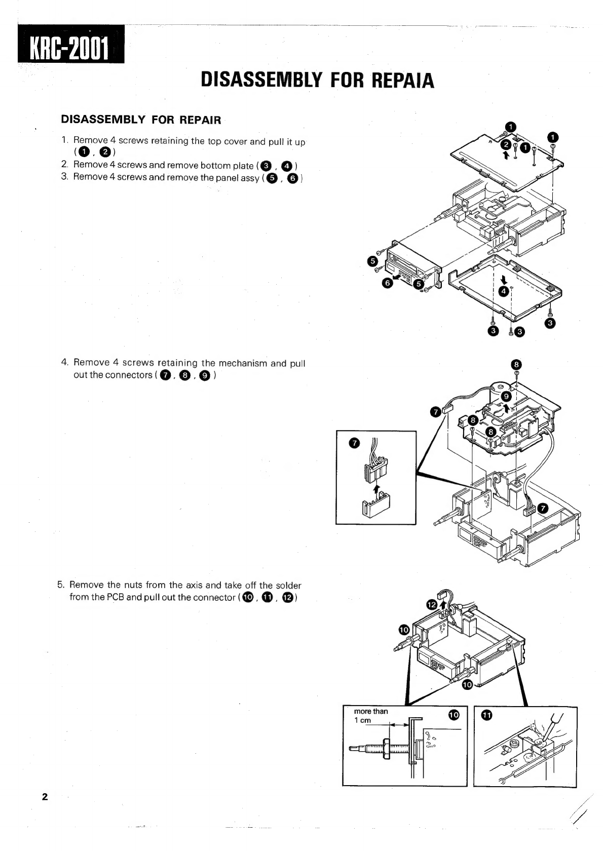
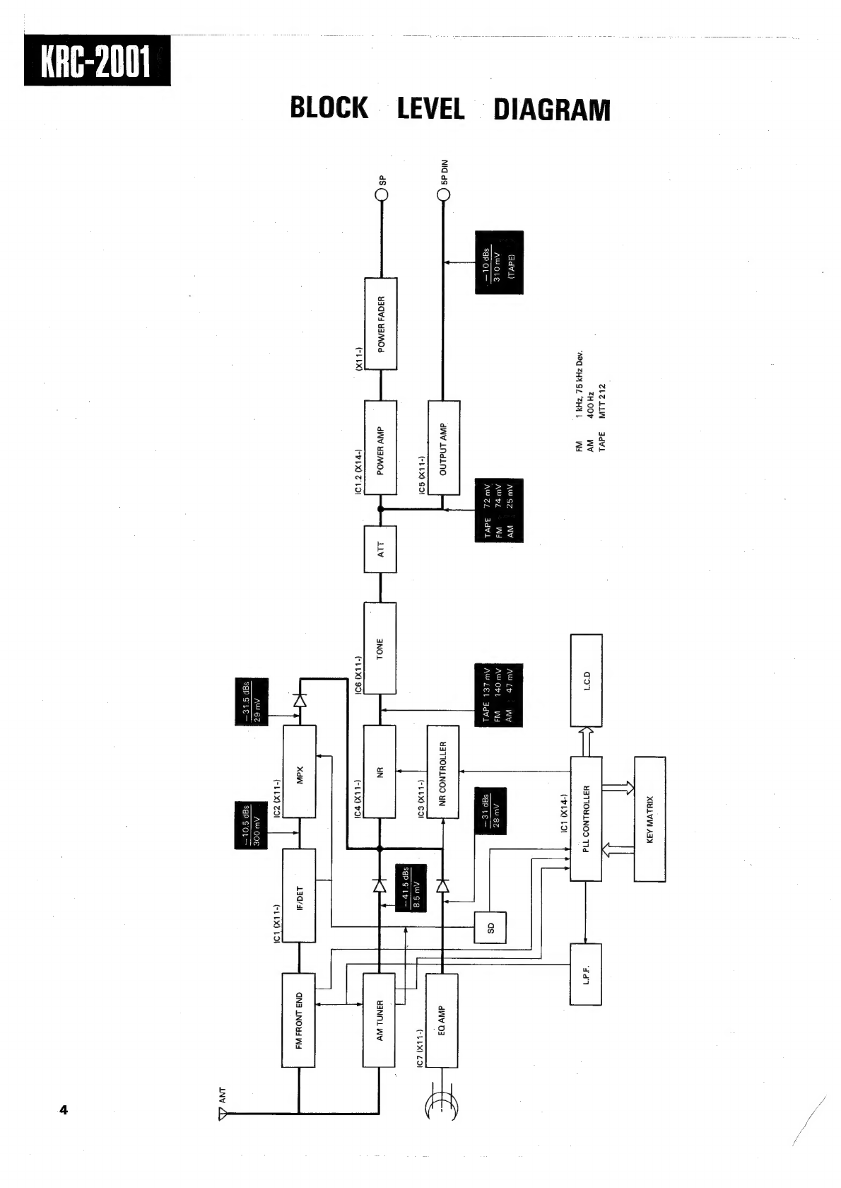
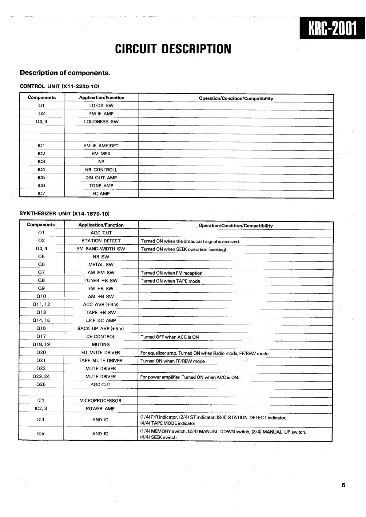
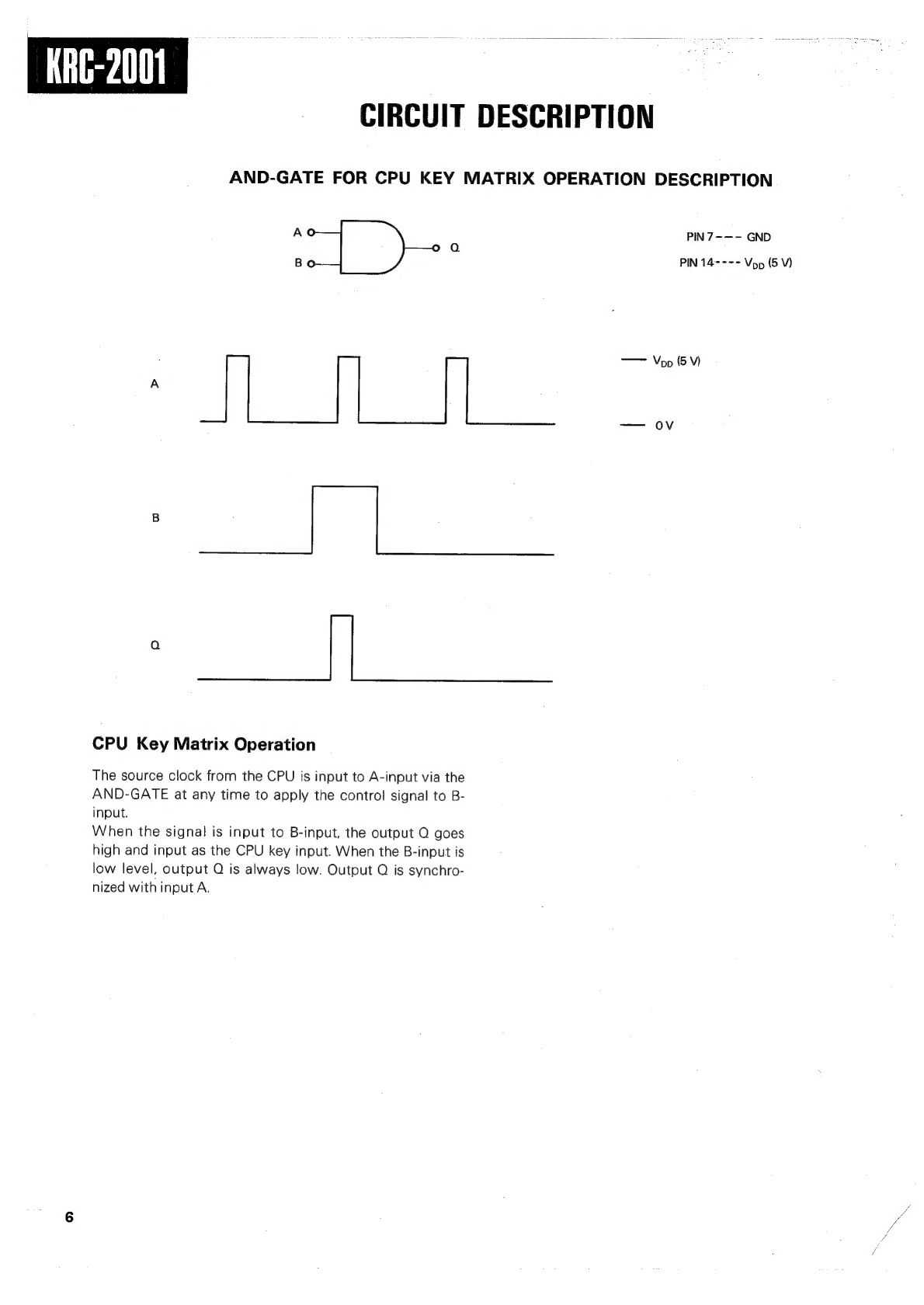
Kenwood KRC-2001 User manual

KENWOOD
KRG-200'
STEREO
CASSETTE
RECEIVER
Knob
Knob Knob
ob
Kn
:
188804)
(K27-1581-04)
(K27-1580-04)
(K27-1579-04)
—
{K29-1
889-04)
Knob
Dressing
pane!
LCD
Assy
Knob
(K29-1888-04)
(A21-0493-03)
(B38-0066-05)
(K29-1888-04)
Heat
sink
(FO1-0681-03)
E
'
2
e-
—-————-
Cord
with
connector
(E30-1430-15)
Cord
with
plug
(E30-1429-05)}
Cord
with
DIN
connector
(E30-1431-15)

ee
DISASSEMBLY
FOR
REPAIA
DISASSEMBLY
FOR
REPAIR
1.
Remove
4
screws
retaining
the
top
cover
and
pull
it
up
(0.8)
2.
Remove
4
screws
and
remove
bottom
plate
(‘O.
8)
3.
Remove
4
screws
and
remove
the
panel
assy
4,
Remove
4
screws
retaining
the
mechanism
and
pull
©
out
the
connectors
(@,.@.@)
©
5.
Remove
the
nuts
from
the
axis
and
take
off
the
solder
from
the
PCB
and
pull
out
the
connector
(@.
@.
®)
more
than
Tem

|
KRG-2001_
DISASSEMBLY
FOR
REPAIA
6.
Pull
out
the
PCB
from
the
bottom
main
PCB
(®.
@.
®)
7.
Removes
the
screw
of
display
assy
(
(B
)
and
remove
six
screws
of
heat
sink(
@&
.
)
Remove
the
screw
(
&®
)
and
pull
out
the
connector
®
(@
)
8.
Remove
the
screws
(
@)
)
and(
@
)

XIMLVW
Aa
ZLZLINW
Adv
ZHOOv
wy
ao7
=z
Y3TIONLNOD
Tid
"A8Q
ZH4
GL
‘ZH
L
W4
‘S47
(adv)
Augc
WV
AWip
WV
AWOLE
AW
oZ
W4
AUOPL
WI
AY
8Z
SaPOL—
AWTL
AdvL
AYLEL
3IdVL
sap
t€—
Nid
ds
()
dV
LNdLno
HATIONLNOO
YN
(-L
LX)
Got
[f
dy
03
H-
eae
(LEX)
£91
ma
=
Y¥aNNL
WV
dS)
¥yadvs
WaMOd
dINV
H3MOd
iv
3NOL
Q
bul
(-L
LX)
(-VLX)
2°
LOt
(-LLX)
994
(-L
LX)
vol
<I
XdN
130/dl
QN3
LNOY4
Wd
(-L
LX)
291
(-LLX)
LOI
BLOCK
LEVEL
DIAGRAM
AU
6S
AW
OO
sgP
SLE—
sap
GOt—
inv
ZN

)
KRe-2001
CIRCUIT
DESCRIPTION
Description
of
components.
CONTROL
UNIT
(X11-2230-10)
Components
Application/Function
_
Operation/Condition/Compatibility
Qi
LO/DX
SW
Q2
FM
IF
AMP
LOUDNESS
SW
FM
IF
AMP/DET
FM
MPX
NR
NR
CONTROLL
DIN
OUT
AMP
TONE
AMP
EQ
AMP
SYNTHESIZER
UNIT
(X14-1870-10)
Application/Function
Operation/Condition/Compatibility
AGC
CUT
ee
OT
ey
|_a2_
|
~_STATION
DeTECT
|
Tuned
ONWhenthebroadcastsignalisreceved.
}__03,4
|
FM
BAND-WIDTH
SW
|
Tuned
ONwhen
SEEK
operation
seeking)
pa
OR
NS
ee
ee
i
OR
NETS
ee
eo
eel
|
os
ag
TUNER
+B
SW
Turned
ON
when
TAPE mode
FM
+B
SW
Q10
AM
+B
SW
Q11,
12
ACC
AVR
(+9
V)
Q13
TAPE
+B
SW
L.P.F
DC
AMP
BACK
UP
AVR
(+5
V)
CE-CONTROL
MUTING
EQ
MUTE
DRIVER
TAPE
MUTE
DRIVER
MUTE
DRIVER
MUTE
DRIVER
AGC
CUT
Turned.
OFF
when
ACC
is
ON
For
equalizer
amp.
Turned
ON
when
Radio
mode,
FF/REW
mode.
Turned
ON
when
FF/REW
mode
For
power
amplifier.
Turned
ON
when
ACC
is
ON.
MICROPROCESSOR
POWER
AMP
(1/4)
F/R
indicator,
(2/4)
ST
indicator,
(3/4)
STATION
DETECT
indicator,
(4/4)
TAPE
MODE
indicator
(1/4)
MEMORY
switch,
(2/4)
MANUAL
DOWN
switch,
(3/4)
MANUAL
UP
switch,
(4/4)
SEEK
switch
AND
IC
AND
IC

KRC-2001
CIRCUIT
DESCRIPTION
AND-GATE
FOR
CPU
KEY
MATRIX
OPERATION
DESCRIPTION
A
PIN
7-—-
GND
a
B
PIN
14*---
Vpp
(5
V)
—
Vpp
(5
Vv)
A
—
OV
B
Qa
CPU
Key
Matrix
Operation
The
source
clock
from
the
CPU
is
input
to
A-input
via
the
AND-GATE
at
any
time
to
apply
the
control
signal
to
B-
input.
When
the
signal
is
input
to
B-input,
the
output
Q
goes
high
and
input
as
the
CPU
key
input.
When
the
B-input
is
low
level,
output
O
is
always
low.
Output
Q
is
synchro-
nized
with
input
A.

CIRCUIT
DESCRIPTION
Synthesizer
Unit
u.-Com:
«PD
1708G
FUNCTION
OUTLINE
Receiving
frequency,
Channel
spacing,
Reference
frequency,
Intermediate
frequency
FM
band
Frequency
range
Channel
spacing
Reference
frequency
Intermediate
frequency
87.9
~107.9
MHz
200
kHz
25
kHz
10,700
87.50~108.0
MHz
*
60
kHz
12.5
kHz
10,700
*
MANUAL
25
kHz
AM
band
Frequency
range
Channel
spacing
Reference
frequency
Intermediate
frequency
530
~
1620
kHz
10
kHz
10
kHz
450
kHz
522~1611
kHz
9kHz 9kHz
450
kHz
163~281
kHz
*
QkHz
1
kHz
450
kHz
*
MANUAL
1
kHz
Tuning
Function
{1)
Auto
Tuning
(Sawtooth
wave
mode)
Seek
Up:
Once
a
station
is
tuned,
it
is
held
tuned.
(2)
Manual
Tuning
(Sawtooth
wave
mode)
Manual
Up/Down:
Frequency
is
advanced
up
or
down
in
steps
by
pressing
the
push
switch.
Pressing
for
a
half
second
or
more
advances
it
up
or
down
continuously
until
the
switch
is
released.
(3)
Preset
Memory
Recall
6
stations
on
each
FM,
MW,
and
LW
band
can
be
preset
independently
with
the
6
buttons.
The
last
sta-
tion
is
stored
in
memory
for
each
band
when
power
is
turned
off.
Tape
Function
(1)
Tape
running
indicator
(2)
METAL
control
(3))
DOLBY
contro!
Radio
Function
(1)
LOC
(local)
contro!
(2)
MONO
control
Clock
Function
(1)
12-hour
display
Other
Functions
(1)
LOUDNESS
control
(2)
NR
(noise
reduction)
control

KAC-2001
CIRCUIT
DESCRIPTION
TERMINAL
DESCRIPTION
Terminal
Configuration
(Top
View)
[+7
26
a
P)
7)
24
[+23
ees
PY
uPD1708G-618-00
p21
(TOP
VIEW)
[_____}
20
[___}19
fT
C—i*d‘O'V
dA
16
[715
14
Pin
Name
Pin
Name
LCD4
KS,
(PB,}
LCD3
KS,
(PBo)
LCD2
BANDZ/N.R
LCDi
METAL-LOC
COM2
LOUDNESS
COM1
5G
|e
|e
|~|o
lor]
a]
|
|=
CE
*
Xl
XO
AF
MUTE
(PA3)
BAND
1
(PA,)
KS,/K;
(PA,)
KS,/K,
(PA,)
Ks
Ky
K,
Ko
KS,
(PB,)
KS,
(PB,)
8
*
Not
used.

Pin
description
KRG-2001
CIRCUIT
DESCRIPTION
Pin
Name
Description
LCD
segment
signal
LCD
segment
signal
output
pin
(1/2
duty,
1/2
bias
LCD
should
be
used.
Frame
frequency:
100
Hz,
Drive
voltage:
VDD)
LCD
common
signal
LCD
common
signal
output
pin
Power
input
Device
power
supply
pins
During
device
operation,
5
V
+
10%
voltage
is
supplied
via
these
pins.
Either
of
them
can
be
used
for
supplying
the
power
individually.
The
rising
time
of
VDD
should
be
less
than
500
ms
(0
to
4.5
V).
When
the
rising
time
is
too
long,
or
when
the
VDD
is
not
lowered
completely
to
O
V
and
then
raised
to
4.5
V
from
the
voltage
lower
than
the
operating
rate,
the
diode
switch
condition
for
initialization
is
not
read
out
correctly.
In
such
cases,
use
the
CE
pin
so
that
the
diode
switch
status
can
be
read
out
for
initialization.
FM
VCO
input
This
pin
inputs
the
FM
station
output
signal.
Since
it
incorporates
the
AC
amp,
cut
the
DC
signal
with
the
capacitor.
AM
VCO
input
This
pin
inputs
the
AM
station
output
signal.
Since
it
incorporates
the
AC
amp,
cut
the
DC
signal
with
the
capacitor.
Ground
Connect
to
the
ground
terminal
of
the
set.
Error
Out
AF
MUTE
Charge
pump
output
of
the
phase
detector
consisting
of
PLL.
When
the
frequency
divided
by
the
oscillating
frequency
is
higher
than
the
reference
frequency,
these
pins
output
high
level
signals,
and
when
it
is
lower
than
the
reference
frequency,
they
go
low.
When
the
frequency
(divided
by
the
oscillating
frequency)
is
coincided
with
the
reference
frequency,
it
enters
into
the
floating
status.
Chip
Enable
Crystal
resonator
Mute
Out
This
pinis
used
to
input
the
selected
signal
from
the
device.
When
operating
the
PLL
section,
this
pin
goes
high,
and
when
the
PLL
section
is
stopped,
it
goes
low.
When
at
low
level,
the
display
goes
off.
However,
a
low
level
signal
below
134
us
or
high
level
signal
is
not
accepted.
Connectors
of
the
crystal
resonator.
Connect
the
4.5
MHz
crystal
resonator.
This
pin
outputs
the
muting
signal
to
eliminate
shock
noise
when
the
PLL
is
unlocked
and
pop
noise
when
switching
between
Tape
and
Radio,
and
is
active
low.
(CMOS
output)
For
timing
details,
refer
to
the
AF
Mute
Out
Timing
Chart.
When
the
CE
pin
is
low,
this
pin
is
active
low.
Band
Out
FM/MW
switching
output
pin
FM:
High
MW:
Low
When
the
MODE
switch
is
set
to
“1”
(Tape
mode),
this
pin
is
low.
When
the
SDK
is
provided,
follow
the
SDK
section.
Key
return
signal
source
and
Key
return
signal
input
This
becomes
the
source
of
key
return
signal
to
read
out
the
diode
matrix
for
initialization
only
when
the
power
is
turned
on
for
the
first
time
(rising
time
of
VDD}
or
when
the
set
is
returned
from
the
back-up
condition
(CE:
Low
to
High).
Then,
this
inputs
the
key
return
signal
for
the
key
matrix.
Insert
the
pull-down
resistor.
(CMOS
input
/output)
Key
return
signal
source
and
Key
return
signal
input
This
becomes
the
source
of
the
key
return
signal
to
read
out
the
diode
matrix
for
initialization
only
when
the
power
is
turned
on
for
the
first
time
(VDD
rising
time)
or
when
returning
from
the
back-up
condition
(CE
goes
high
from
low).
Then,
this
inputs
the
key
return
signal
for
the
key
matrix.
Insert
the
pull-down
resistor.
{CMOS
input
/output)
Key
return
signal
input
This
pin
inputs
the
key
return
signal
for
the
key
matrix.
Insert
the
pull-down
resistor.
(CMOS
input)
Key
return
signal
source
This
pin
outputs
the
key
return
signal
for
the
key
matrix.
Since
the
synchronous
current
is
greatly
lowered
because
of
its
configuration,
the
reverse-current
prevention
diode
will
be
not
necessary
for
the
key
source
side.
(CMOS
output)
METAL/DX/LOC
|
LOC
Out
In
radio
mode:
DX/Local
On/Off
output
pin
When
“LOC”
is
displayed
on
the
LCD
panel,
high
level
signal
is
output.
When
it
is
not
lit,
low
level
signal
is
output.
(When
the
power
is
turned
on,
low
level
status
is
initialized.)
In
tape
mode:
METAL
On/Off
output
pin
When
“METAL”
is
displayed
on
the
LCD
panel,
low
level
signal
is
output.
When
it
is
not
lit,
high
level
signal
is
output.
On
initialization
when
the
tape
power
is
turned
on,
high
level
is
output.

10
CIRCUIT
DESCRIPTION
Pin
Name
Symbol
Description
LOUDNESS
Loudness
Out
LOUDNESS
output
pin
When
“LOUD”
is
displayed
on
the
LCD
panel,
low
level
signal
is
output.
When
it
is
not
lit,
high
level
signal
is
output.
When
the
power
is
turned
on
first
(VDD
rising
time),
low
tevel
signal
is
output.
(CMOS
output)
BAND2/NR
When
Band
A
is
“0”
or
“1”
and
the
NR
selector
is
“1”,
this
functions
as
the
NR
on/off
output
pin.
When
“NR”
is
dis-
played
on
the
LCD
panel,
high
level
signal
is
output.
When
it
is
not
lit,
low
level
signal
is
output.
This
pin.can
be
operated
in
the
TAPE/RADIO
mode.
On
initialization
when
the
power
is
turned
on,
this
pin
is
at
low
level.
When
BAND
A
is
“0”,
“1”
and
the
NR
selector
is
“O”,
this
function
as
the
WIDE-ADV
on/off
output
pin.
@
Inthe
Radio
mode:
This
functions
as
the
WIDE
on/off
output
pin.
When
“WIDE”
is
displayed
on
the
LCD
panel,
high
level
signal
is
output,
and
when
it
is:
not
lit,
low
level
is
output.
DOLBY
output
pin
When
“DOLBY”
is
displayed
on
the
LCD
panel,
high
level
signal
is
output.
When
itis
not
lit,
low
level
signal
is
output.
On
initialization
when
the
power
is
turned
on,
low
level
is
output.
@
Inthe
Tape
mode:
This
functions
as
the
ADV
on/off
output
pin.
When
“ADV”
is
displayed
on the
LCD
panel,
high
level
signal
is
output,
while
it
is
not
lit,
low
level
is
output.
On
initialization
when
the
power
is
turned
on
first,
it
is
at
low
level.
When
BAND
A
is
“0”
and
the
NR
selector
is
“O”
(SDK
oper-
ation
is
normal
only
when
in
this
status),
and
BAND
B
is
“1”,
this
pin
functions
as
the
BAND
2
output.
BAND
2
be-
comes
the
band
switching
output
port
in
combination
with
BAND
1.
Output
BAND
1
BAND
2
ee
ee
Ne

mS
KAC-2001
CIRCUIT
DESCRIPTION
1.
KEY
MATRIX
CONFIGURATION
1-1.
Key
Matrix
Layout
The
SSS
in
the
SSS
shows
the
pin
no.
L
|
:
Momentary
switch
:
Alternate
switch
or
transistor
switch
Zi
:
Diode
matrix
(ieee
suaned
by
diode)
-
1-2.
Switch
Connection
Momentary
switch
Alternate
switch
Diode
matrix
or
open
Transistor
switch
Kn
Kn
Kn
Vop
Kn
KSm
KSm
KSm——
KSm
i
11

KRC-2001
CIRCUIT
DESCRIPTION
1-3.
Key
Matrix
Connection
:
Momentary
switch
:
Alternate
switch
or.transistor
switch
:
Diode
matrix
oo
>
wPD1708G-018-00
or
pPD1708G-218-03
KS,/K,
KS,/K,
12

KRG-2001
CIRCUIT
DESCRIPTION
2.
KEY
MATRIX
DESCRIPTION
(1)
The
switch
for
setting
the
receiving
frequency
range
and
the
channel
spacing:
2-1.
Diode
Matrix
for
Initialization
BAND
A
The
diode
matrix
for
initialization
has
the
following
five
status.
All
status
is
read
out
only
when
the
power
is
sup-
(2)
Clock
signal
select
switch:
plied
to
the
Vpp
for
the
first
time
(Power-ON,
Reset)
and
CLKSEL
when
the
CE
pin
goes
high
from
low
level
(CE
Reset),
in
another
periods,
the
diode
matrix
status
is
ignored.
(3)
Priority
select
switch
for
display:
PRIORITY
(4)
—
(5)
NR
select
switch:
NR
SEL
(6)
CLOCK/FREQUENCY
select
switch:
CLOCK/FRO
(7)
LW
select
switch:
BAND
B
Symbol
Function
Description
This
switch
is
used
for
setting
the
receiving
frequency
range
for
each
FM/MW/LW
band
channel
spacing.
Each
setting
status
is
as
follows:
BAND
A
BAND
A
Frequency
Range
Channel
Spacing
Manual
Step
:
|
1
|
87.9~107.9MH2
2oorkz
|
=
|
1
|
s30~te20KH
|
torte
|
|
o
|
87.
p
25kHe
|
522~1611
kHz
When
the
clock
function
is
provided,
this
switch
selects
the
priority
mode
for
display.
When
the
display
which
does
not
have
priority
is
recalled,
the
mode
having
priority
will
be
displayed
after
approx.
PRIORITY
5
seconds.
“1:
No
priority
; :
“0”:
Priority
is
provided.
,
g75~1080MHz
|
—
SOkHz
:
Select
switch
to
provide
the
clock
function
or
not.
CLKSEL
“1”:
Clock
is
not
provided
(For
back-up,
RAM
is
not
cleared)
;
“0”:
Clock
is
provided.
Select
switch
to
provide
the
NR
(noise
reduction)
function.
“0”:
NR
is
not
provided
(WIDE-ADV
and
BAND
2
output
pin)
“1:
NR
provided
Select
switch
to
provide
priority
to
the
clock
or
frequency
for
display
(Depending
on
PRIORITY)
CLOCK/FRQ
“O":
Frequency
“1:
Clock
Switch
to
access
the
preset
memory
(M1
to
M6)
sequentially
“0”:
M1
to
M6
keys
are
preset
independently
“1”:
Each
time
the
M1
key
is
pressed,
preset
memory
is
sent
sequentially
CM
Mey
13

KRG-2001
CIRCUIT
DESCRIPTION
2-2.
Mode
Select
Switches
Unlike
the
initializing
switches,
these
switches
can
be
changed
at
any
times.
(On
the
following
table,
“1”
shows
switched
ON,
“O”
shows
switched
OFF)
Function
Description
Set
the
unit
to
RADIO
mode
or
TAPE
mode.
“1°:
TAPE
mode
“O":
RADIO
mode
In
the
RADIO
mode:
This
is
the
Station
Detector
input
in
SEEK
or
SCAN
mode.
SD
This
should
be
set
to
OFF
within
approx.
50
ms
after
the
PLL
is
locked.
When
every
times
are
OFF
by
detecting
the
station
every
1
ms,
the
station
is
recognized
as
received
and
the
seeking
or
scanning
operation
stops.
In
the
RADIO
mode:
(Only
for
FM
reception)
Stereo
signal
input
switch.
When
this
switch
turns
OFF,
“ST”
is
displayed
on
the
LCD
panel.
However,
“ST”
goes
off
in
the
Auto
Tuning
mode
(AF.
MUTE
pin
is
active)
even
if
this
switch
is
OFF.
STEREO
In
the
Tape
mode:
Tape
running
direction
indicator
input
switch.
When
this
switch
turns
ON,
the
“REV”
(<4)
is
displayed
on
the
LCD
panel.
When
it
tums
OFF,
the
“FOW"
(bP)
is
displayed,
This
switch
functions
only
when
the
CE
pinis
high
and
the
MODE
switch
is
“ON”
(Tape
mode).
FOW/REV
2-3.
Momentary
Switches
Symbol
Function
Description
These
keys
are
used
for
manual
tuning
and
time
adjustment.
@
Frequency
display
Each
time
the
key
is
pressed,
the
displayed
frequency
is
advanced
up
(by
MU
key)
or
down
(by
MD
key)
by
1
step
(channel
spacing
set).
When
it
is
pressed
for
a
half
second
or
more,
the
frequency
is
advanced
rapidly
(continuously)
until
itis
released.
,
@
Clock
(time)
display
While
pressing
the
ME
key,
press
the
MD
key
to
adjust
the
time,
and
press
the
MU
key
to
adjust
minutes.
In
the
Radio
mode:
These
keys
are
used
to
write
or
recall
the
preset
memory.
FM,
MW
and
LW
bands
can
be
stored
independently
into
each
key
inmemory.
(1)
When
writing
With
the
frequency
display,
within
five
seconds
after
pressing
the
ME
key,
press
one
key
(M1
to
M6),
to
store
the
fre-
quency
currently
received
into'memory.
(2)
When
recalling
When
one
key
(M1
to
M6)
is
pressed,
the
memory
content
(frequency)
corresponding
to
the
key
pressed
is
recalled,
When
the
radio
is
turned
on
after
the
VDD
is
first
turned
on,
the
lowest
frequency
on
the
FM
band
is
recalled.
When
shipped,
the
following
frequencies
are
preset
into
M1
to
M6
key
for
adjustment
at
the
factory.
87.9~107.9
MHz
87.50~108.00
MHz
530~1620
kHz
522~1611
kHz
14
|
y.

Y
KRC-2001
CIRCUIT
DESCRIPTION
Function
Description
Symbol
These
keys
are
used
to
write
and
recall
the
preset
memory.
Each
FM,
MW
and
LW
frequency
can
be
stored
into
one
key
in
memory
independently.
However,
the
number
of
available
bands
differ
with
the
area
designated
by
the
initializing
diode
matrix,
as
follows:
For
the
area
only
2
bands
are
available:
6
stations
*
2
=
12
stations
For
the
area
3
bands
are
available:
6
stations
X
3
=
18
stations
Corresponding
to
the
preset
key
pressed,
the
‘CH’
indicator
and‘*
”
(channel
number)
are
displayed
on
the
LCD
panel.
Mi
5
M6
These
keys
are
used
for
automatic
tuning.
During
auto
tuning
operation,
when
the
SD
switch
is
turned
OFF,
the
frequency
displayed
at
the
time
is
kept
on
hold.
In
auto
tuning
mode,
the
auto
tuning
operation
is
continued
even
when
the
LOUDNESS,
ME,
NR,
METAL-DX/LOC,
or
MONO-DOLBY
key
is
pressed.
When
one
of
the
other
keys
is
pressed,
the
auto
tuning
operation
is
stopped,
and
the
unit
enters
the
operation
of
the
key
pressed.
When
the
SEEK
key
is
pressed
again,
the
frequency
before
the
SEEK
operation
is
resumed.
This
key
is
used
to
select
the
function
between
DX/LOC
—
MTL.
@
Inthe
Radio
mode:
Each
time
the
key
is
pressed,
the
LOC
output
pin
and
the
“LOC”
display
on
the
LCD
panel
are
inverted.
When
the
“LOC”’
display
on
the
LCD
panel,
high
level
signal
is
output
from
the
LOC
Out
pin,
and
when
it
is
not
lit,
low
level
is
output.
@
Inthe
Tape
mode:
.
Each
time
the
key
is
pressed,
the
LOC
output
pin
and
the
“MTL”
display
are
inverted.
When
the
“MTL”
is
displayed
on
the
LCD
panel,
low
level
signal
is
output
from
the
LCD
Out
pin,
and
when
it
is
not
lit,
high
level
is
output.
By
initialization
when
the
power
is
turned
on,
high
leve!
signal
is
output.
SEEK
UP/DOWN
DX/LOC
—MTL
This
key
is
used
for
writing
the
preset
memory.
It
is
also
used
for
adjusting
the
time
on
clock
display.
@
Frequency
display:
Used
when
writing
a
new
frequency
into
the
preset
memory.
When
this
key
is
pressed,
the
‘‘ME”
is
displayed
on
the
LCD
panel,
and
lit
for
five
seconds
after
the
key
is
released.
While
the
“ME”
is
lit,
pressing
one
key
(M1
to
M6)
stores
the
displayed
frequency
into
memory
corresponding
to
the
key
pressed.
To
cancel
the
preset
memory,
while
the
“ME”
is
lit,
press
any
key
other
than
ME,
NE,
METAL-DX/LOC,
MONO-DOLBY,
or
LOUDNESS.
®
Clock
display:
The
“hour”
and
‘“‘minutes”
can
be
adjusted
by
pressing
the
MD
or
MU
key
while
pressing
the
ME
key.
After
pressing
the
ME
key,
each
time
the
MD
key
is
pressed,
the
“‘hour’’
is
advanced
one
by
one.
Pressing
it
for
a
half
second
or
more
advances
the
time
by
4
hours/sec
continuously
until
the
MD
key
is
released.
This
operation
does
not
affect
the
“minute”
or
“second”
digits
(they
are
not
displayed
during
this
operation).
After
pressing
the
ME
key,
each
time
the
MU
key
is
pressed,
the
‘“minute”’
is
advanced
one
by
one.
Press
it
for
a
half
second
or
more
advances
the
minute
in
8
minutes/sec
speeds
continuously,
unti!
the
MU
key
is
released.
The
“second”
is
not
displayed,
however,
it
is
reset
to
zero
every
time
the
“minute”
is
set.
The
‘‘minute”
adjusting
does
not
affect
the
“hour”.
(“Hour’
is
not
changed
even
when
the
“‘minute’’
exceeds
60.)
(During
clock
display,
pressing
the
ME
key
alone
changes
the
display
to
frequency
and
“ME”
is
displayed.
In
this
condition,
pressing
one
of
the
preset
keys
(M1
to
M6)
stores
the
frequency
into
the
memory
corresponding
to
the
key
pressed.)
This
key
is
used
to
select
the
band.
When
Band
A
is
“O”
or
“1”
and
Band
B
is
“0”
(LW:
Not
available)
. . .
Each
time
this
key
is
pressed,
the
band
is
changed
in
the
order
of
FM
—
MW
—
FM...
Used
for
Loudness
select
key.
Each
time
this
key
is
pressed,
the
loudness
output
pin
and
the
“LOUD”
display
on
the
LCD
panel
are
inverted.
When
the
“LOUD”
is
displayed
on
the
LCD
panel,
low
level
signal
is
output
from
the
Loudness
pin
and
when
it
is
not
lit,
high
level
is
output.
By
initialization
when
the
power
is
first
turned
on
{rising
time
of
VDD),
“LOUD”
is
displayed
and
low
level
is
output.
LOUDNESS
15

KRE-2001
|
16
CIRCUIT
DESCRIPTION
Function
Description
Display
select
key.
Available
only
when
in
the-radio
mode.
When
this
key
is
pressed,
the
display
is
changed
from
the
clock
display
to
frequency
or
vice
versa.
However,
five
seconds
after
the
key
is
pressed,
the
display
is
restored
to
the
priority
mode
(depending
on
the
diode
matrix
PRIORITY).
When
the
clock
is
not
provided
(CLKSEL=0),
this
key
has
no
effect.
However,
the
clock
display
is
resumed
by
the
PRIORITY
switch
when
the
display
priority
is
provided.
a)
ON:
Priority
is
provided
b)
OFF:
No
priority
(1)
NR
key
(RADIO/TAPE
common
key)
(2)
WIDE-ADV
key
(Independent
RADIO/TAPE
key)
(1)
NR
key:
BAND
A:
“0”,
1”
NR
SEL:
1"
With
the
above
status,
this
key
is
used
as
the
NR
select
key.
Each
time
the
key
is
pressed,
the
BAND2/NR
output
pin
and
“‘NR”
display
on
the
LCD
panel
are
inverted.
When
“NR”
is
displayed
on
the
LCD
panel,
the
BAND2/NR
pin
outputs
the
high
level,
and
when
the
display
is
not
lit,
low
level
is
output.
(By
initialization
when
the
power
is
turned
on,
it
outputs
low
level.)
(2)
WIDE-ADV
key:
BAND
A:
“0”,
"1°"
NR
SEL:
“1”
With
the
above
status,
this
key
is
used
as
the
WIDE-ADV
select
key.
In
the
Radio
mode:
Used
as
the
WIDE
select
key.
7
Each
time
the
key
is
pressed,
the
BAND2/ADV
output
pin
and
the
“WIDE”
display
on
the
LCD
panel
are
inverted.
When
the
“WIDE”
is
displayed
on
the
LCD
panel,
the
BAND2/ADV
pin
outputs
the
high
level,
and
when
the
display
is
not
lit,
low
level
is
Output.
On
Tape
mode:
Used
as
the
ADV
select
key.
Each
time
the
key
is
pressed,
the
BAND2/NR
output
pin
and
the
“ADV”
display
on
the
LCD
panel
are
inverted.
When
the
“ADV”
is
displayed
on
the
LCD
panel,
the
BAND2/NR
pin
outputs
the
high
level.
When
the
display
is
not
lit,
the
low
level
is
output.
{By
initialization
when
the
power
is
turned
on,
low
level
is
output.)
Note:
When
the
following
status
is
selected
in
the
diode
matrix,
the
NR
key
and
the
WIDE-ADV
key
are
not
effective.
NR
SEL:
“0”
BAND
A:
“0”
BAND
B:
“1”
This
key
is
used
for
setting
the
received
frequency
range
for
FM/MW/LW
band
and
the
channel
spacing.
1.
By
initialization
when
the
power
is
turned
on,
the
receiving
frequency
and
channel
spacing
are
registered
by
the
diode
of
BAND
A.
Then,
when
the
CE
pin
goes-*L"’—"‘H“or
vice
versa,
they
follow
the
diode
of
BAND
A.
2.
When
the
CE
pinis
inverted
to
high
from
low
while
pressing
the
M5
key
and
the
BAND
key
together,
the
band
setting
of
BAND
A
is
changed
from
“1”
to
“O”
or
from
“0”
to
“"1"".
Then,
when
the
CE
pin
is
inverted
toc*L"’—>“H’4or
vice
versa,
the
changed
area
setting
is
maintained.
3.
When
the
CE
pin
is
inverted
from
low
to
high
while
pressing
the
M5
key
and
BAND
key
together,
the
band
setting
follows
the
diode
of
BAND
A.
Then,
when
the
CE
pinis
inverted
fromL’’—“H“or
vice
versa,
it
follows
the
diode
of
BAND
A,
too.
4.
To
change
the
setting
by
the
M5
key
and
the
BAND
key,
repeat
procedure
2
and
3.
Note:
On
initialization
when
the
power
is
turned
on,
the
M5
key
and
the
BAND
key
are
ignored
even
when
they
are
pressed,
and
the
setting
is
followed
to
the
diode.
M5
BAND

Set
the
controls
and
switches
as
follows.
BALANCE
:center
position
FADER
:center
position
BASS
scenter
position
TREBLE
:center
position
ITEM
LOUD
T+
ADY
METAL
DOLBY
NR
:
INPUT
SETTINGS
OFF
:
OFF
OFF
OFF
ADJUSTMENT
LOCAL
AUTO
OUTPUT
SETTINGS
OFF
:
OFF
TUNER
(RECEIVER)
SETTINGS
ALIGNMENT
POINTS
ALIGN
FOR
SECTION
(A)
Connect
the
98.
1MHz
DC
voltmeter
FM
0
dev
between
pins
98.
1MHz
60dBCANT
input)
of
TP1
(A)
Connect
the
98.
1MHz
frequency
FM
0
dev
counter
pins
98.
1MHz
60dBCANT
input)
of
TP2
(C)
98,
1MHz
lkHz,#67.5kHz
dev
(B)
Selector:L
or
R
60dB(ANT
input)
CA)
98.
1MHz
FH
0
dev
98,
1MHz
20dBCANT
input)
(A)
98.
1MHz
FH
1kHz,275kHz
dev
98.
1kHz
BOdBCANT
input)
ANT
OPEN
FM
(No_signal)
98.
1kHz
DISCRIMINATOR
19,
00kHz
Adjust
it
so
that
the
FH
crosstalk
from
L
to
R
and
98.
1MHz
R
to
L
become
minimum,
SEPARATION
STOP
LEVEL
{__
SOFT
MUTE
Set
the
volume
to
0
dBs,
SOFT
MUTE
|
VRi
990kHz
AM
vR1
~
25dBs
-_—_i__
@)
STOP
LEVEL
400Hz,30%
mod
990kHz
(X14)
STOP
38dBCANT
input)
SSETTE
DECK
SECTION
zo
Adjust
the
azimuth
for
each
|
L-CH/R-CH
or
FOW/REV
becomes
maximum,
Head
Azimuth
Screw
TAPE
PLAY
AZIMUTH
MTT-
114
(10kHz)
17

REGLAGE
Regler
les
controles
et
les
boutons
comme
suit.
BALANCE
:position
centre
LOUD
:OFF
LOCAL
:
OFF
FADER
:position
centre
T-
ADV
:0FF
AUTO
:OFF
BASS
:position
centre
METAL
:OFF
TREBLE
:position
centre
DOLBY
NR
:OFF
REGLAGE
DE
REGLAGE
DE
REGLAGE
DU
TUNER
POINTS
DE
ITEM
L’
ENTREE
LA
SORTIE
CAMPLI-TUNER)
|
L’
ALIGNEMENT
ALIGNER
POUR
CTION
MF
Raccorder
le
CA)
volimetre
CC
DISCRIMINATEUR
98,
1MHz
entre
les
deux
Fi
0
dev
broches
de
98,
1MHz
60dBCEntree
ANT)
TPL
(AD
Raccorder
le
98,
MHz
compteur
de
0
dev
frequence
aux
19,
00kHz
60dBCEntree
ANT)
|
broches
de
TP2
(C)
98,
MHz
Le
regler
de
maniere
SEPARATION
1kHz.267,5kHz
dev
(B)
FH
a
ce
que
la
diaphonie
Selecteur:L
ou
R
98,
1MHz
deLaR
et
de
Ra
L
60dBCEntree
ANT)
devienne
minimum.
CA)
NIVEAU
98,
\MHz
FM
D’
ARRET
0
dev
98,
LMHz
ARRET
20dB(Entree
ANT)
(A)
98,
1MHz
FH
SILENCIEUX
DOUX
LkHz.275kHz
dev
98,
MHz
Regler
le
volume
a
0
dBs.
(1)
60dBCEntree
ANT)
SILENCIEUX
DOUX
Quvrir
1’
antenne
FM
(pas
de
signal)
98,
1MHz
—
25dBs.
(D)
NIVEAU
990kHz
AX
D’
ARRET
400Hz.
30%
mod
990kHz
38dBCEntree
ANT)
CTION
DU
MAGNETPHON
—T
Ajuster
1’
azimut
pour
que
AZIMUTH
MTT-
114
Lecture
bande
Vis
d’
azimut
de
chaque
L-CH/R-CH
ou
(10kHz)
tete
FOW/REY
devienne
maximum.
18
/

KRG-2001
KRG-2001
ABGLECH
ADJUSTMENT/REGLAGE/ABGLECH
Die
Regler
und
Knopfe
wire
folgt
einstellen.
BALANCE
:Mittelage
LOUD
:
OFF
LOCAL
:
OFF
FADER
—-:Mittelage
T+
ADV
:OFF
AUTO
SOFE
BASS
:Mittelage
METAL
:OFF
TREBLE
:Mittelage
DOLBY
NR
:OFF
EINGANGS-
AUSGANGS-
TUNER
CRECEIVER)-
ABGLEICH
GEGENSTAND
EI
NSTELLUNG
EINSTELLUNG
EINSTELLUNG
PUNKTE
ABGLEICHEN
FuR
WOABTEILUNG
w
;
Den
Gieichstron-
(A)
Voltmeter
98,
1MHz
zwischen
den
)
(c)
DISKRIMINATOR
0
Hub
beiden
Stif-
.
60dBCANT-
Eingang)
ten
von
TPL
anschliegen.
(D)
(A)
Den
Frequenzzahler
98,
1MHz
an
die
Stifte
FM
0
Hub
von
TP2
98,
IMHz
19,
O0kHz
60dBCANT-
Eingang)
anschliegen,
(Cc)
98,
1MHz
So
einstellen,
dag
das
STEREO
KANAL
1kHz.#67,5kHz
Hub
(B)
:
FM
wbersprechen
von
TRENNUNG
Wahler:L
oder
R
98,
1MHz
L
auf
R
und
60dBCANT-
Bingang)
von
R
auf
L
minimal
wird.
aii
(8)
a
|
98,
1MHz
FM
a
:
HALT
PEGEL
0
Hub
98,
LMHz
HALT
vanes
Oscilloscope
E
20dBCANT-
Eingang)
Wechselspan-
Oscilloscope
°
r
(C)
nungsmesser
2
ae
z
Weiche
Dampfung
98,
1MHz
FM
Die
Lautstarek
i
qd)
1kHz.275kHz
Hub
98,
1MHz
auf
0
dBs
einstellen.
|
60dBCANT-
Bi
ngang)
Weiche
Dampfung
|
Die
Antenne
offnen
FH
Speaker
|
(2)
(Kein
Signal).
98,
IMHz
;
to
ANT
-ABTEILUNG
(D)
990kHz
MY
HALT
PEGEL
400Hz.
80%
mod
990kHz
38dBCANT-
Bingang)
SSETTEN-DECK-—-ABTEIL
So
einstellen,
dag
das
Azimuth
fur
jeweils
AZIMUTH
MTT-
114
(1
0kHz)
Bandwiedergabe
Kopfazimutschraube
|
~
L-CH/R-CH
oder
FOW/REV
maximal
wird.
(f)
VR1
SOFT
MUTE
AM
STOP
LEVEL
DISCRIMINATOR
(c)
VR4
SEPARATION
e
a
(b)
VR5
vco
(h)
Head
Azimuth
Screw
19

20
&
0.
bE
oF
z
a.
77)
&
6
wee
a
«
ve
9°
zs
Ga
uw
rr cc
a
of
4
el
a)
ao}
of
=|
[fx]
3]
«= e]
)&
2}
§|
SLUS
a)
2
3|
3
~)
WHT
5
CONTROL
(X11-2230-10
B/5)
KRC-2001
KRG-2001
PC
BOARD
DIN
cE
GND
LR
SP
Component
side
view
SYNTHESIZER
(X14-1870-10)
3!
3
JT
BRN
RED
1
oO
ORG
76
_
Zz
oO
ac
Le
XII
C/5
CONTROL
(X11-2230-10
C/5)
in
C23
°
Ql
B38-0066-05
LCD
ASSY
CONTROL
(X11-2230-10
A/5)
Component
side
view
ANT
PLAY/BACK
HEAD
CONTROL
(X11-2230-10
D/5)
Refer
to
the
schematic
diagram
for
the
values
of
resistors
and
capacitors.
The
PC
board
drawing
is
viewing
from
the
side
easy
to
check.
Table of contents
Other Kenwood Stereo Receiver manuals

Kenwood
Kenwood KR-4070 User manual

Kenwood
Kenwood KR-5200 User manual

Kenwood
Kenwood R-V251 User manual

Kenwood
Kenwood 103AR User manual

Kenwood
Kenwood AR-304 User manual

Kenwood
Kenwood KRC-754 D User manual

Kenwood
Kenwood KRF-V8070D User manual

Kenwood
Kenwood VR-716 User manual

Kenwood
Kenwood KR-V7040 User manual

Kenwood
Kenwood KRF-V5020 User manual

Kenwood
Kenwood KR-V888D User manual

Kenwood
Kenwood KRF-V4070D User manual

Kenwood
Kenwood KRF-V7771D Manual

Kenwood
Kenwood KR-7600 User manual

Kenwood
Kenwood VR Series User manual

Kenwood
Kenwood 103AR User manual

Kenwood
Kenwood VRS-6100 User manual

Kenwood
Kenwood KR-9600 User manual

Kenwood
Kenwood DVR-6200 User manual

Kenwood
Kenwood KR-596 User manual