144/440(430)MHz
FM
DUAL
BANDER
TH-77A/E
SERVICE
MANUAL
KENWOOD
©1990-8
PRINTED
IN
JAPAN
B51-8057-00(B)1105
————
CONTENTS
DISASSEMBLY
FOR
REPAIR.........:cscssceccscssssesesesseessseessvess
2
CIRCUIT
DESCRIPTION
...ccscccsscsccssesssseecesecsesesseessesenseensssee
4
DESCRIPTION
OF
COMPONENTS.
......cccescccscsesssseecsseeeene
16
SEMICONDUCTOR
DATA.
......cccsscssssescecseccescessesssecrecsersese
20
PARTS
LIST....ccsccsscsocscscssecsssescsssccsseessseeees
Be
ete
tee
29
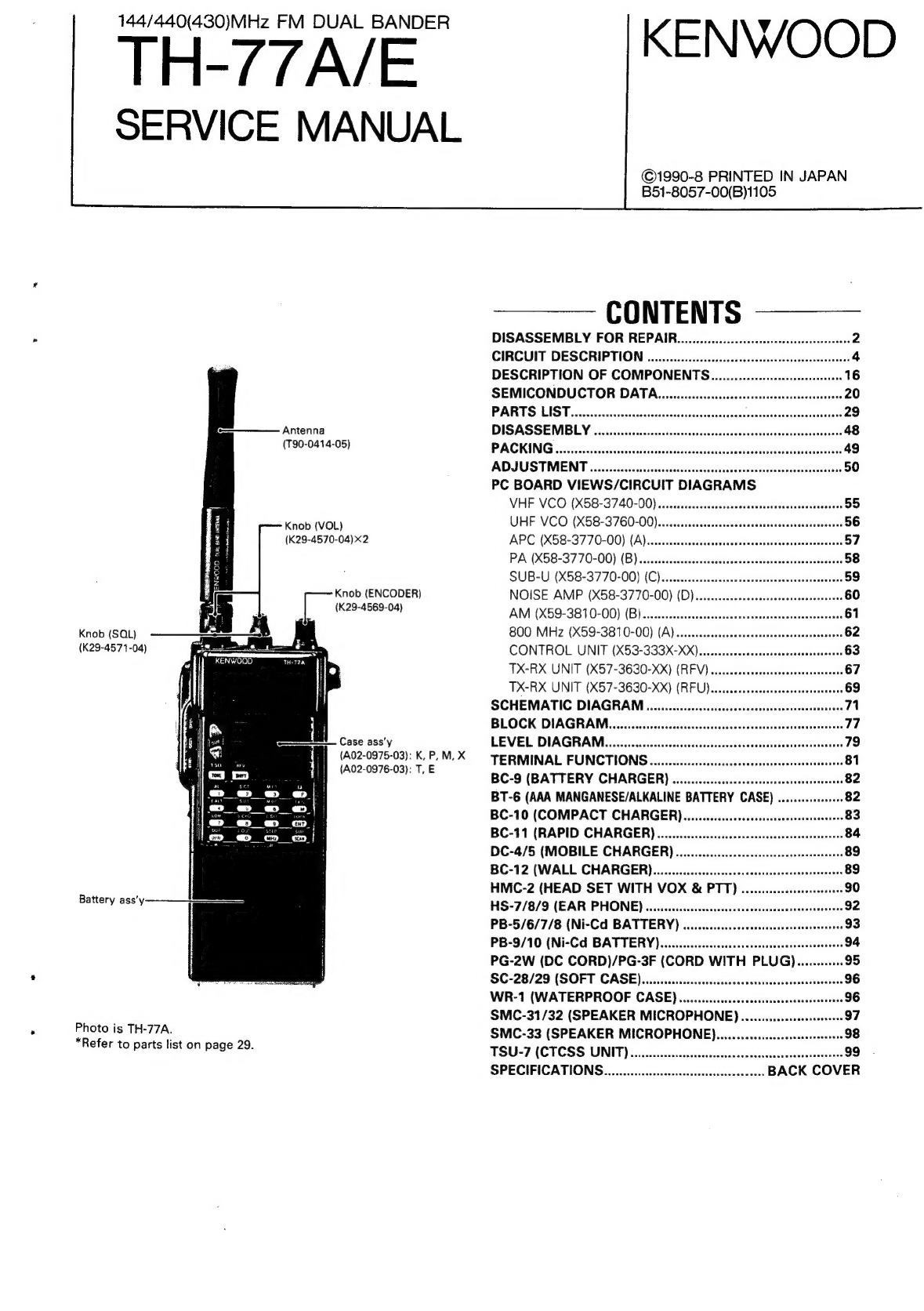
Antenna
DISASSEMBLY
............0...ccccccecccssccessesssceescecsesenseseeccceneneees
48
(790-0414-05)
PAGKING
250.
ei.cs0cg:hs
accaceligseralisedsiuvitdessangdaoucaseverbicecseeteor
49
ADJUSTMENT
.......cssccssssssccssecccscsccsscsssececsecsusceracsnseesncessese
50
PC
BOARD
VIEWS/CIRCUIT
DIAGRAMS
-%
VHF
VCO
(X58-3740-00)
...ccssscsucccossccessececsrsnscneesnecsrseecses
55
bi
nen
Wvar)
UHF
VCO
(X58-3760-00)..-cssssscsovessssesossevssssscersessessecocesss
56
|
(K29-4570-04)x2
APC
1K502077
0-00)
(AVS
itect
aks
ots
ce
canes
57
|
be
PI,
(H5B597.70-0G)
1B)
cscavtasceetsdesescssaestanoeetasncivtencbtehes
58
SUB-U
(X59-37
70-00):
(Chsscacsercescctevadvivervesissnasnasosavsersie
59
Knob
(ENCODER)
NOISE
AMP
(X58-3770-00)
(D).ccccsecccesssseecsseccessseecneeereee
60
ie
Neo
aeee
4)
AM
(X59-3810-00)
(B)
..ssssscsssssssesscsvecessecaressnessescneecenesssse
61
Knob
(SQL)
.
f
B00
MHz
(X59-3810-00)
(A)
.sessssssssesecesecesessscsseersessssensees
62
(K29-4571-04)
ee
eet
CONTROL
UNIT
(X53-333X-XX)..ssssesceeeessssseeseessceseeneeees
63
Pee
TX-RX
UNIT
(X57-3630-XX)
(REV)
.vscesssseeersvesseestsesseeeses
67
|
TX-RX
UNIT
(X57-3630-XX)
(RFU)
.scsccessecsesccsecsecersseessves
69
SCHEMATIC
DIAGRAM
u....ccsscssscsecccsssscsecsseseuseseecacceeseesee
71
BLOCK
DIAGRAM......cscssscsssessssscscsseccsessesecstesrsesseenssesseesses
77
——"
ee
lee
cores
LEVEL
DIAGRAM.................cccccccccereeseccecceccssessccceececerseesees
79
-0975-03):
K,
P,
M,
TERMINAL
FUNCTIONS
..0....ccsscssssscscccesssecssssessesssssseenseess
81
ep
a
ie
BC-9
(BATTERY
CHARGER)
..ccccccccsssscssscccsssssssssceveeessooe
82
BT-6
(AAA
MANGANESE/ALKALINE
BATTERY
CASE)
.................
82
BC-10
(COMPACT
CHARGER).........cccscsesessssescesssssessesssees
83
cis
i
BC-11
(RAPID
CHARGER)
.........cccccscsscsosecsescssesceccucsseereees
84
wu
DC-4/5
(MOBILE
CHARGER)............ccscsceccscssesseceueeseesseres
89
BC-12
(WALL
CHARGER)........cccscsssssccsesesesssssessesssessseenees
89
HMC-2
(HEAD
SET
WITH
VOX
&
PTT)
...scscsssessssessesssees
90
Battery
ass’y
HS-7/8/9
(EAR
PHONE)
............::cccsccsecceeeeesecssteeneenseeesenens
92
PB-5/6/7/8
(Ni-Cd
BATTERY)
.....sccsscsscesecsssccctsesssssseessses
93
PB-9/10
(Ni-Cd
BATTERY)
....c.ccssccoscssecesecseecssscasssccsseeseess
94
PG-2W
(DC
CORD)/PG-3F
(CORD
WITH
PLUG)............
95
SC-28/29
(SOFT
CASE)
...cccccessscsessssssscececsessscsesseecasessecesess
96
WR-1
(WATERPROOF
CASE)
.......cccscscececesssssccseecesecsesssees
96
SMC-31/32
(SPEAKER
MICROPHONE)
...........:++e-02e000++-
97
Photo
is
TH-77A.
SMC-33
(SPEAKER
MICROPHONE).........0...ccssecsssssseesoee
98
eter
to
parts
list
on
page
29.
TSU-7
(CTCSS
UNIT)
cesccssccsssssccssssssssessssccsssesscsssseeeeveee
99
SPECIFICATIONS.
.........ccsssessssssseeeetessseeeceees
BACK
COVER


