manuals.online logo
Brands
  1. Home
  2. •
  3. Brands
  4. •
  5. Kenwood
  6. •
  7. Transceiver
  8. •
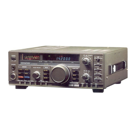
  9. Kenwood TS-440S Instruction manual

Kenwood TS-440S Instruction manual

Other manuals for TS-440S

10

Other Kenwood Transceiver manuals

Kenwood TH-22A User manual

Kenwood

Kenwood TH-22A User manual

Kenwood NEXEDGE NX-720 User manual

Kenwood

Kenwood NEXEDGE NX-720 User manual

Kenwood TR-9130 User manual

Kenwood

Kenwood TR-9130 User manual

Kenwood TH-27A User manual

Kenwood

Kenwood TH-27A User manual

Kenwood NEXEDGE NX-248 User manual

Kenwood

Kenwood NEXEDGE NX-248 User manual

Kenwood TM-411A User manual

Kenwood

Kenwood TM-411A User manual

Kenwood TK-3130 - ProTalk XLS UHF User manual

Kenwood

Kenwood TK-3130 - ProTalk XLS UHF User manual

Kenwood TH-28E User manual

Kenwood

Kenwood TH-28E User manual

Kenwood TS-520S User manual

Kenwood

Kenwood TS-520S User manual

Kenwood TS-700SP User manual

Kenwood

Kenwood TS-700SP User manual

Kenwood UBZ-LH14 User manual

Kenwood

Kenwood UBZ-LH14 User manual

Kenwood TS-B2000 Operating manual

Kenwood

Kenwood TS-B2000 Operating manual

Kenwood TK-7160 User manual

Kenwood

Kenwood TK-7160 User manual

Kenwood TS-930S User manual

Kenwood

Kenwood TS-930S User manual

Kenwood TS-530SP User manual

Kenwood

Kenwood TS-530SP User manual

Kenwood NEXEDGE NX-900 User manual

Kenwood

Kenwood NEXEDGE NX-900 User manual

Kenwood TK-840 User manual

Kenwood

Kenwood TK-840 User manual

Kenwood TM-2550A User manual

Kenwood

Kenwood TM-2550A User manual

Kenwood TK-7360 User manual

Kenwood

Kenwood TK-7360 User manual

Kenwood TK-5220 K User manual

Kenwood

Kenwood TK-5220 K User manual

Kenwood TK-2160 User manual

Kenwood

Kenwood TK-2160 User manual

Kenwood TK-3000 K User manual

Kenwood

Kenwood TK-3000 K User manual

Kenwood TS-480HX Manual

Kenwood

Kenwood TS-480HX Manual

Kenwood TH-22A User manual

Kenwood

Kenwood TH-22A User manual

Popular Transceiver manuals by other brands

City Theatrical SHoW DMX SHoW Baby user manual

City Theatrical

City Theatrical SHoW DMX SHoW Baby user manual

Standart Horizont HX407 owner's manual

Standart Horizont

Standart Horizont HX407 owner's manual

B&G V90S quick start guide

B&G

B&G V90S quick start guide

VictelGlobal ALK300 series Operation manual

VictelGlobal

VictelGlobal ALK300 series Operation manual

Cactus Wireless Flash Transceiver V6 user manual

Cactus

Cactus Wireless Flash Transceiver V6 user manual

Yaesu FT-11R user guide

Yaesu

Yaesu FT-11R user guide

Skanti TRP 5000 instruction manual

Skanti

Skanti TRP 5000 instruction manual

ELECRAFT KX3 Installation and operation guide

ELECRAFT

ELECRAFT KX3 Installation and operation guide

American Lighting DMX512 quick start guide

American Lighting

American Lighting DMX512 quick start guide

Furuno FM-77 Operator's handbook

Furuno

Furuno FM-77 Operator's handbook

Yaesu FT-7B manual

Yaesu

Yaesu FT-7B manual

Mizuho MX-2 Operating & assembly instruction

Mizuho

Mizuho MX-2 Operating & assembly instruction

Blitz MJ-398U instruction manual

Blitz

Blitz MJ-398U instruction manual

Utilicom LongRanger 2050 Operator's manual

Utilicom

Utilicom LongRanger 2050 Operator's manual

Standart HX290UKA Service manual

Standart

Standart HX290UKA Service manual

Altronix Pace1PTM installation guide

Altronix

Altronix Pace1PTM installation guide

Kirisun PT2208 instruction manual

Kirisun

Kirisun PT2208 instruction manual

ELECRAFT KX2 manual

ELECRAFT

ELECRAFT KX2 manual

manuals.online logo
manuals.online logoBrands
  • About & Mission
  • Contact us
  • Privacy Policy
  • Terms and Conditions

Copyright 2025 Manuals.Online. All Rights Reserved.

KEN WOO
D
T
S-440SPS-430SP-4a
0
SPECIFICATIONS

2
HF TRANSCEIVE
R
CONTENT
S
CIRCUIT DESCRIPTION

4
SEMICONDUCTORS

27
PARTS LIST

3
5
PC BOARD SCHEMATIC DIAGRA
M
SWITCH UNIT

6
9
FILTER UNIT

70, 7
1
PLL UNIT

72, 7
3
RF UNIT

74, 7
5
CONTROL UNIT

76, 7
7
DISPLAY UNIT

76, 7
7
FINAL UNIT

78
IF UNIT

78, 7
9
AT UNIT

80
DISASSEMBLY

81
PACKING

8 8
ADJUSTMENT

8
9
LEVEL DIAGRAM

10
1
BLOCK DIAGRAM

10
3
OPTIO
N
PS-50

104
PS-430

109
VS-1

1 1
1
SP-430

11
4
MB-430

11
4
AT-440

11
4
YK-88S /S N

11
4
YK-88C/CN

11
4
SCHEMATIC DIAGRAM

113
TS-440
S
(GENERAL
)
Transmitter frequency range
:
Receive frequency range
:
Mode
:
Antenna impedance
:
Power requirement
:
Power consumption
:
RX no signal input
:
TX
:
Frequency configuration
:
RX unit
:
TX unit
: (A1,A3J,A3,FSK
)
(F3
)
Semiconductors
:
SPECIFICATION
S
160m BAND
1
.8 —
2
.0MH
z
80m BAND
3
.5 —
4
.0MH
z
40m BAND
7
.0 —
7
.3MH
z
30m BAND
10
.1

—
10
.15MH
z
20m BAND
14
.0

--
14
.35MH
z
17m BAND
18
.068 — 18
.168MH
z
15m BAND
21
.0 — 21.45MH
z
12m BAND
24
.89 — 24
.99MH
z
10m BAND
28
.0 — 29
.7MHz
100kHz — 30MH
z
Al (CW), A3J(SSB), A3(AM), F1 (FSK), F3(FM
)
50 Ohm (TX
: 20— 150 Ohm with AT
)
12
.0--
16
.0V D
C
Approx
. 1
.9
A
Approx
. 20
A
1st IF 45
.05MHz, 2nd IF 8.83MHz, 3rd IF 455kH
z
1st IF 455kHz, 2nd IF 8
.83MHz, 3rd IF 45
.05MH
z
1st IF 36
.22MHz, 2nd IF 45
.05MH
z
CW, SSB, AM, FSK, FM
: Triple conversion superheterodyn
e
FM
: Double conversion superheterodyne
TS-440S
TS-440S (with AT
)
Tr's
1 57
1 7
4
FET's
22
2 2
IC's
49
5 8
Diod's
257
27
7
(
TS-440S TS-440S

with AT
)
W(mm)
270 (279)
270 (279
)
H(mm)
96 (108)
96 (108
)
D(mm)
313 (335)
313 (335
)
Weight(kg)
6
.3
7
.
3
Dimensions
:
(
The numbers in the parenthesis include protections
.
(TRANSMITTER
)
Ratead final power input
:
Carrier supression
:
Unwanted sidebande supression
:
Harmonic content
:
Transmit frequency character
:
Maximum frequency diviation (FM)
:
Microphone impedance
:
More than 40d
B
More than 50d
B
Less than
-40d
B
400--2600Hz (—6dB
)
±5k H
z
50052 - 50k
g
2
TS-440
S
SPECIFICATION
S
(RECEIVER
)
Sensitivity
:
Freq
.
Mode
100 -- 150kHz
150

500kHz
0
.5 --

1
.6MHz
1
.6 -- 30MH
z
SSB,CW,FS
K
(SIN10dB)
Less tha
n
2
.5µV
(8dBA1
Less tha
n
1µV (OdB
A
)
Less tha
n
4µV (12dBA)
Less tha
n
0
.25µV (— 12dB
A
)
AM (SIN 10dB)
Less tha
n
25µV
(28dBp) Less tha
n
13µV (22dB
A
)
Less tha
n
40/,cV
(32dBA)
Less tha
n
2
.5µV
(8dBA
)
FM (12dB SINAD)
Less tha
n
0
.7µV (—3 dBµ
)
Squelch
sensitivity
: (Threshold
)
Mode
•

•
150 -- 500kHz
0
.5 —

1
.6MHz
1
.6 - - 30MH
z
SSB,CW,AM,FSK
Less tha
n
20AV (26dBA1
Less tha
n
10
A
V (20dBp)
Less tha
n
20µV
(26dBA)
Less tha
n
2µV (6dBA
)
FM
Less tha
n
0 32
A
V (— 10d B
A
)
Image ratio
:
IF rejection
:
Selectivity
:
IF SHIFT variable range
:
RIT/XIT variable range
:
Audio output power
:
Audio output impedanc
e
(FREQUENCY STABILITY
)
Frequency accuracy
: (RIT/XIT OFF
)
Frequency stability
:
(RIT/XIT OFF
: at receive
)
Reference oscillator frequency
:
50dB or more (1 00kHz -- 1 6MHz
)
70dB or more (1
.6 — 30MHz
)
50dB or more (FM 3rd image ratio
)
50dB or more (100kHz --- 1 6MHz
)
70dB or more (1
.6MHz -- 30MHz
)
Fre
d
Mode
— 6dB — 60d
B
SB,CW,FSK
More than 2kHz Less than 4
.4kH
z
AM
More than 4kHz
Less than 18kHz (— 50dB
)
FM
More than 1 2kHz Less than 25kHz (— 50dB)
±0
.9kHz or mor
e
± 1 kHz or mor
e
1
.5W or more (with 8S2 load, 10% distortion
)
4 — 1652 (Speaker and headphone
)
More than
±10
x 1
0
-
6
More than
±10
x 10
-6
(— 10°C to 50°C
)
36MH
z
Note
:
Circuit and ratings subject to change without notice due to developments in technology
.
3
TS-440S
CIRCUIT DESCRIPTIO
N
1
. Overview
•
The TS-440 is a triple conversion type transceiver, incor-
porating a general coverage receiver, which uses 45
.0
5
MHz as the first IF, 8
.83 MHz as the second IF, and 45
5
kHz as the third IF
.
•
The TS-440 is compact, but allows for installation of a
n
optional internal automatic antenna tuner operating in th
e
amateur band from 3
.5 MHz to 28 MHz and enables
a
wide range of antennas to be used
.
•
The TS-440 also contains a microprocessor-controlled dig-
ital PLL circuit which controls frequency in 10 Hz step
s
using a single crystal oscillator to implement high accura
-
cy and stable frequency control
.
•
The TS-440 has the following major features
:
(1)
Selectable VFOs
; VFO-A and VFO-
B
(2)
Direct frequency input using a numeric keypa
d
(3)
100-channel memory containing frequency band
,
and mode information (channel 90 to 99 for split fre
-
quency memory
)
(4)
Memory scan in 10 channel groups and two type
s
of program sca
n
(5)
RTTY (AFSK) mode availabl
e
(6)
Squelch circuit operational in all mode
s
(7)
Dual filters available to improve selectivity and SI
N
ratio (optional filter required
)
(8)
IF shift, audio notch, IF filter switching, and RF AT
T
functions for convenient interference reductio
n
(9)
Large heat sink and cooling fan (100 W) enabling u
p
to one-hour continious transmit operatio
n
(101 Full and semi break-in circuits for C
W
(1 1) External-computer controllable (optional interface re
-
quired
)
(12) Many easy-to-read meter functions such as th
e
received signal strength (s-meter), transmitter power
,
SWR, and ALC level
.
2
. Frequency Element
s
The TS-440 utilizes a triple conversion transmitter an
d
receiver
.
V
30K

f IN
RX MIX
1
30MHz ,

RX
TX
45
.05MHz RX MIX2
8
.83MHz
RX MIX3
455KHz
DE
T
DISCR I
RX OUTPU
T
TX MIX3
TX MIX
I
8
.83MH
z
TX MIX
2
SSB,CWT, AM,
FM, FSK
(FM MOD
)
:45
.O8^-75
.05MH
z
-CW R

:45
.0792-- 75
.0492 MHz
SS B
C
W
FS
K
'
AMR,FM
R
AMT,FMT
: 455KH
z
USB,
CW

:
456
.5
KH
z
-LSB,FSK

453
.5KH
z
FSK
AFS INPU
T
B
.M
.
SS
B
AM
MIC INPU
T
F
M
Fig
. 1
Frequency configuratio
n
The overall frequency configuration of the TS-440 is show
n
in Figure 1
. The incoming received signal (f,
N
l
is applied t
o
the ANT terminal
. This signal is mixed with the local oscilla-
tor signal (fvco) in RX MIX 1 to obtain the first IF frequen-
cy
. This signal is then mixed with the HET Oscillator signa
l
(fHET) in RX MIX 2, to obtain the 2nd IF frequency
. Th
e
resulting signal is then mixed with the second local oscilla
-
tor frequency (f
L
o) to obtain the 3rd IF frequency
. The sig-
nal is then combined with the CAR signal for detection
. f
i
N
is expressed mathematically as follows
:
fiN = fvco

fHEr – fLo

fcAlt

1
4
TS-440
S
CIRCUIT DESCRIPTIO
N
ANT
Fig
. 2 PLL frequency configuratio
n
30
K
30MHz

1st MIX
MIX
3rd MI
X
2nd
D
AF OU
T
DE
T

/

\
I

5 KHZ

I

6
.22MHZ

P
D

120KHZI

1= 1800 1=450
1
J=72441=1811
1
FM
MOD


I
/
1
I

HI

IPLL 5
1
I I F
M
MIX 5
4
.55MH
AMR,FM
R
AMT, FMT

: 455 KH
z
USB, CW

: 456
.
5
LSB,
FSK

: 453
.
5
CA
R
1/1
0
IX 4
9
.9—10 4MH
1/2
0
1/
5
IPLL
31
I/1
0
MKR —
(=13720_
.20719)
1 1
RIT, XI
T

Y
I/L

11/180
0
L=19800
`_
MN614
7
20799

4
P
.D
99=104MH
z
(98_6 =103
.6MHZ
)
—
5KHZ
—

I
M=323
9
299 4
STEP 5
)Cw
R
1
/P
o
r
I
/P-
I
F
P
I/1
---
-
7006 J
58
.25-
u
53
.25MHz
BP
F
r
1
I

p,D

I/
M
}
20KH
Z
1/450
AM,FM

: 91 MH
z
USB,CW

: 91
.3 MH
z
LSB,FSK
: 90
.7MH
z
IPLL4I

I
AM,FM

: K=1820
0

USB,

CW

K=1826
0
LSB,FSK

K=1814
0
IPLL
11
D

I/N,I/A--L
1
8
SOOKHZ

INT=13-
.73

T _ MN614
7
NT=PN-A

L—

—

I
91 MH
z
/'
—
1
I
.98^-2
.08MH
z
64
.78
=
59
.88MHz
P
.D
5KH
z
I/K
1/180
0
—
As shown in figure 2, all received frequencies excluding th
e
local oscillator frequency fLo are generated in the PLL circuit
.
The frequencies generated in these loops are expressed a
s
follows
:
-
fsT
D
VC04
:
f
K04
4
800 •
. fvco4 = 7200 fSTD
...
3
.fsTD


L

VCO3
: fvLos =
4
800

fvcos = 7200 fSTD
....
4

fvcoz + fvco3 + fvco4

1
'fsT
D
50

20

4
M

45 0

M

fsTD

fvco
_ s

fvco4

5
fvcoz = 1800

50

2
0
VC01
:
N

1
8
:
.
fvcos = 72 fSTD + fLo +
f
STD
f
1
002
. .
6
Based on these formulas, the frequencies fvcor fHET, and
fCA
R
are expressed as follows
:

/
N

M

L

fvco
= fvcor =
(
72

1800 + 3600000
K
+ 1440000 + 1) fsTD + fLo

7
J
f
HET = fVCO5 = 41

fSTD

8
Formula 1 may now be rewritten as follows
:
N _

M

L

J
fIN 1
72

180000 + 3600000

41 +
1
)
.
fsT
D

1
0
Note that f
L
o
is
not included in formula 10
. That is,
a
received frequency is determined by the reference frequen-
cy fs
TD
and frequency division data
Ito
N
. Further analysi
s
of formula

10 shows the following
:
i)
Basically, frequency division data I to N contain no er-
ror because they are controlled by the microproces-
sor according to the operating frequency
.
ii)
The accuracy of the operating frequency is equal t
o
that of the reference frequency, because all frequen-
cies other than fs
TD
in formula 10 are determine
d
by the microprocessor
.
iii)
The operating frequency does not change even if k o
r
fLo changes
.
When f
IN
= 14 MHz (USB mode) in formula 10 , f
IN
an
d
f
STD have the following relationship
:
VCO5
:
fvcos

4 fsTD
fvcos =
J

I

4
1
fSTD

2
VCO2
:
fvcos — f
L
o — fSTD + fvcoz

1
f
10

4
sTD
fvco4

K
fcAR

200

1440000
fSTD

9
5
TS-440S
CIRCUIT DESCRIPTIO
N
I=1800, J=7244, K=19800, L=3239, M=4
1

fin = 0
.388 fsTD

1 1
When fIN = 30 MHz (USB mode) in formula 10 , f
IN
an
d
fSTD have the following relationship
:
I = 1800, J = 7244, K = 19800, L = 3239, M = 7
3

.'
. fIN = 0
.833
f
STD

1
2
Since the precision of the reference crystal oscillator use
d
in the TS-440 is 10 ppm (—10 to 50°C) and the receive
r
system has the characteristics shown in items i) and ii), th
e
total accuracy is stable at any point from 30 kHz to 30 MHz
.
The maximum amount of frequency shift is only +/— 30
0
Hz (see formula 12 )
. The characteristic shown in ite
m
iii) enables variable band functions such as IF shift to be im
-
plemented, using the microprocessor. The microprocesso
r
also is used to set carrier points by adjusting fcAR, and to se
t
and adjust the amount of IF shift
.
So far received frequencies in the SSB mode have been dis
-
cussed
. For receive modes other than SSB, and in transmi
t
mode, operating frequency is determined by the referenc
e
frequency and frequency division data
.
In CW receive mode,
fvco
is shifted down 800 Hz and use
d
as
fvco3
.
In AM or FM receive mode, fCAR generation i
s
stopped
. In FM receive mode, f
HET
is modulated by addin
g
audio signals to VCO5 from the microphone
. FSK (RTTY) i
s
transmitted in LSB mode and uses AFSK by adding audio sig
-
nals externally
.
The type of frequency displayed differs, depending on th
e
mode, as shown in Table 1
.
Mode
Displayed frequenc
y
USB, LSB, FS
K
C
W
AM, FM
Carrier point frequenc
y
Transmission carrier frequenc
y
IF filter center frequency
Table 1 Displayed frequencie
s
3
.
Receiver Circuit Descriptio
n
IC
2
C335
7
f
I F AMP
.
DE
T
Noise
S
O
CF
3
CFW455
Fig
. 3 Receiver circuit configuratio
n
CF I
Q7,
8
3SK73GRx2
IC
7
µPC2002V
S P
SSB
C
.F
AF P
A
CF
2
C
.
F
6
TS-440
S
CIRCUIT DESCRIPTIO
N
t
Signals from the ANT pin are fed into the RAT pin of the R
F
unit via the transmit/receive switching relay
. The signals the
n
go to the 10 BPFs through the approx
. 20 dB attenuator cir
-
cuit, the first stage of the first IF trap circuit, and the lo
w
pass filters (which pass only 500 kHz or less)
. The signal the
n
goes through the second stage of the first IF trap circuit, an
d
is mixed with the VCO signal and converted into the first I
F
signal of 45
.05 MHz in the first mixer, consisting of Q3 an
d
Q4 (2SK125-5)
. The VCO circuit consists of Q21 to Q2
4
(2SC2668Y) and oscillates in four bands from 45
.05 MH
z
to 75
.05 MHz
. Oscillator frequencies are controlled by D
C
signals from the PLL unit
.
The first IF signal of 45
.05 MHz is passed through the MC
F
(F1), which is used in both receive and transmit, and is am
-
plified by the first IF amplifier Q5 (3SK74L)
. In the secon
d
mixer, consisting of Q6 and Q7 (2SK1 25), the first IF signa
l
is mixed with the heterodyne oscillator signal (36
.22 MHz
)
from the PLL circuit, amplified by Q12 (2SC2668Y) to ob-
tain the second IF signal (8
.83 MHz)
. The second IF signa
l
of 8
.83 MHz goes through the gate of the noise blanker
. I
n
modes other than FM , the signal then goes through the MC
F
(F2) and is fed into the IF unit through buffer amplifiers Q
8
and Q9 (2SC2668Y)
.
1) Selectivity circui
t
Figure 4 is a selectivity circuit diagram
. In auto mode, th
e
appropriate bandwidth filter is automatically selected accord
-
ing to mode
. When an optional filter is used, two filters ar
e
available
. Tables 2 and 3 shows the various combinations
When the optional 8
.83 MHz filter is connected, the secon
d
IF signal is then fed from the IF unit into the optional filter
.
In the third mixer, consisting of Q1 and Q2 (3SK73GR), th
e
second IF signal is mixed with 8
.375 MHz signal generate
d
by IF unit's heterodyne oscillator circuit, consisting of Q5
3
and Q54 (2SC2458Y), and converted into the third IF signa
l
(455 kHz)
. The third IF signal is then amplified by Q
5
(3SK73GR)
. A diode switch is used to route the signal t
o
either the FM or SSB circuits
.
In SSB mode, the third IF signal goes through the SSB cer-
amic filter (XF3)
. In AM mode, the third IF signal goes throug
h
the AM ceramic filter (XF4)
. In either mode, the third IF sig-
nal is then amplified by Q7 and Q8 (3SK73GR) and detected
.
In FM mode, the third IF signal goes through the FM cerami
c
filter (XF5)
. The signal is then sent to the FM IF, IC2 (M
C
3357) for amplification and detection
. IC2 also contains a
n
FM noise squelch circuit
.
The detected SSB/AM signal is passed through the notch cir
-
cuit, consisting of hybrid IC IC1 (BX6124) and squelch gat
e
Q12 (2SC2459BL)
. The signal then goes through the A
F
volume control and is amplified to the appropriate level b
y
AF amplifier IC7 (UPC2002V)
.
of bandwidth available when optional filters are used
. In F
M
mode, the selectivity switch does not operate and a singl
e
dedicated FM filter is used
. Optional filters operate only i
n
receive and are separate from the filters used in transmit
.
AUTO SELECTIVITY CONTROL
I
—

X59—1070—00
1
D6

01
I
558
21
,

i
l
a
< ss
R
455 3t_
.
14
/a

D
I
+
R
+
z
'
.
,$W
I
AI
AL
T
D5

02
L a
J
r
p1
<
I
cw
R
R4~~
fro
m
04
IC 1
0
D4
RY
R
D
2
~•
14

i
D3

0 3
Bew

sj

r
l
a
—
i
L_
.
j
J
<A M
R
45A

6L
RX
B

45A
I

DI I

la


Bow
I

o

D
9

M 2
I4
N
-
88
5
455
0
D
5
45S
(
-
a
D8
6
SELEC-
TIVIT
Y
BBC
AUTO
n
AU
T
454
GNDI

F/14
—
J
Fig
.
4
Selectivity control circuit

MANUAL SELECTIVITY CONTROL
7
TS-440S
CIRCUIT DESCRIPTIO
N
Filter selectiv
e
AUTO MODE
WITHOUT OPTION
OPTION INSTALLE
D
MODE
8
.83MHz
455kHz
8
.83MHz
455kH
z
SSB
Through CFI
XF1
CF
1
CW
Through
CF1
XF2
CF
1
AM
Through
CF2
Through
CF
2
FSK
Through
CFI
XF2
CF
I
FM
Through
—
Through
—
XF1:
YK-88S or YK-88S
N
XF2:
YK-88C or YK-88C
N
Table
2
Item
Ratin
g
Center frequency fo
45
.05 MH
z
Center frequency deviation
fo±
1 kHz at 3 d
B
Pass bandwidth
±9
.6
kHz or more at 3 d
B
Attenuation bandwidth
±28
kHz or less at 10 d
B
Ripple
0
.7 dB or les
s
Insertion loss
2
.0 dB or les
s
Guaranteed attenuation
30 dB or more with
±1
MH
z
(Except spurious
)
Final impedance
2 kS1±10 %IL characteristi
c
Table 4 MCF (L71-0259-05) (RF UNIT
Fl
)
Item
Ratin
g
Center frequency fo
8830
kHz±0
.5
kH
z
Pass bandwidth
±3
kHz or more at 3 d
B
Attenuation bandwidth
±12
kHz or less at 18 d
B
Guaranteed attenuation
30 dB or more within
fo±
1
MH
z
Ripple
0
.5 dB or les
s
Insertion loss
1
.0 dB or les
s
Final impedance
2
.5 kfll3 pF
Table 6 MCF (L72-0260-05) (RF unit F2
)
Item
Ratin
g
Center frequency fo
455
kHz±0
.2
kHz at 6 d
B
6 dB bandwidth (total)
± 1
.1
-1
.3
kH
z
60 dB bandwidth
4
.5 kHz or les
s
Guaranteed attenuation
60 dB or mor
e
(at 0
.1
-1

MI-Iz
)
Spurious (600—700 kHz)
40 dB or mor
e
Ripple with bandwidth
2 dB or less at 60 d
B
Insertion loss
2 dB or les
s
Temperature
— 10°C—
+50°
C
Input and output impedance
2
a
l
Table 8 Ceramic filter (L72-0356-05) (IF UNIT CF1)
MANUAL MODE
WITHOUT OPTION
OPTION INSTALLE
D
SELECT
8
.83MHz

455kHz
8
.83MHz
455kH
z
N
NO
RX
XF2
CF
1
XF1
CF
1
M
1
M2
Through
CFI
Through
CF
1
W
Through
CF2
Through
CF2
XF1:
YK-88S or YK-88S
N
XF2:
YK-88C or YK-88C
N
Table
3
Item
Ratin
g
Center frequency fo
455 kH
z
6 dB bandwidth
±2
kHz or mor
e
40 dB bandwidth
7
.5 kHz or les
s
Insertion loss
6 dB or les
s
Guaranteed attenuatio
n
(within 455kHz ±

100kHz)
35 dB or mor
e
Input and output impedance
2
.0
a
l
Table 5 Ceramic filter (L72-0355-05) (IF UNIT CF2
)
Item
Ratin
g
Center frequency fo
455
kHz±1
'kH
z
6 dB bandwidth
±6
kHz or mor
e
50 dB bandwidth
±12
.5
kHz or les
s
Rippl
e
(within 455 kHz±4 kHz)
3 dB or les
s
Insertion loss
6 dB or les
s
Guaranteed attenuatio
n
(within 455 kHz± 100kHz)
35 dB or mor
e
Input and output impedance
2
.0 kS
l
Table 7 Ceramic filter (L72-0315-05) (IF unit CF3
)
Item
Ratin
g
Center frequency fo
8 830 MH
z
Attenuation bandwidth
±50
kHz or more at 3 d
B
Guaranteed attenuation
35 dB or more at 9 285 MH
z
45 dB or more at 9
.74 MH
z
Insertion loss
6 dB or les
s
Ripple
1
.0 dB or les
s
Input and output impedance
330 S
l
Max

voltage (DC)
50 V (Min
l
Table 9 Ceramic filter (L72-0351-05) (IF unit CF4
)
8
TS-440
S
CIRCUIT DESCRIPTIO
N
2)
AF notch circuit
R OH
M
BX7I91— 851
8
123

10
BX719
I
R7 IOK
R9 22
K
OUT!
-
S
C
5

1
0
+
0 iI t
i
U

W
U
D27

D2
6
Fig
. 5 NOTCH circui
t
The hybrid ICI in the IF unit is an audio notch circuit
.
Figure 5 shows its equivalent circuit
. This circuit forms state-
variable band pass filter, also known as a bi-quad filter
. Th
e
notch frequency can be changed using the notch control vari
-
able resistor
. Since the circuit consists of the hybrid IC, sta
-
ble attenuation characteristics can be obtained electrically an
d
thermally
. The range of variable notch frequencies is 400 H
z
to 2600 Hz
.
The notch frequency is determined by the following tw
o
formulas
.
1)
f
N
,,R6/27r (R1 +Notch VR)•R8•R10•C1
.
C65

1
2)
R6
.
1R12+R13)=R10•R11

2
If a variable resistor is used for resistor NOTCH VR, the notc
h
frequency can be controlled according to formula 1)
.
The notch frequency range is from 400 to 2600 Hz, and at-
tenuation is from 25 to 50 dB
.
9
TS-440S
CIRCUIT DESCRIPTIO
N
3
.
Transmitter Circuit Descriptio
n
IC
4
MIC

pPCI
I58HZ

SS
B
D

<M1C AMP
GAI
N
PRO
C
FSK
IN
45
.05^
-
75
.05MH
z
Q4
6
3SK73
Q10,1
I
3SK122 x2
Q13,1
4
3SKI22x
2
F
I
MC
F
Q4
4
2SC2459
IC
5
AN612
CFI
IC
6
AN612
CF
4
IST
MIX
9
.83MH
z
DB
M
ssB
Q1
6
2SC253
8
LP
F
Q
I
2SC2075
02,3

Q4,
5
2SC2509x2 2SC2879x 2
LPF/
-
0
A
.T
R
X
Fig
. 6 Transmitter circuit
configuratio
n
In SSB, CW, AM, or FSK mode, the transmitter system use
s
triple conversion . In FM mode, the transmitter system use
s
double conversion using PLL modulation
.
Audio signals from the microphone are applied to the MI
C
pin (connector (21)) of the IF unit and are separated into SS
B
modulation and VOX signals
. The SSB signal is amplified ap-
prox
. 8 dB by IC4 (µ
.PC 1 1 58HZ)
. AFSK audio signals fro
m
the AFSK IN pin (back panel) are also applied to IC4
.
IC4 functions as a SPEECH processor
. Output from IC4 i
s
distributed to the MIC GAIN control (front panel) and FM cir-
cuit (RF unit)
. In SSB mode, the signal applied to the MI
C
GAIN control is sent back to the IF unit (connector (23) MV2)
,
amplified by Q44 (2SC2459), and supplied to the balance
d
modulator IC5 (AN612)
. In FM or CW mode, Q44 does no
t
operate because a cut-off voltage is supplied to its emitte
r
via diodes D82 and D46 . The signal converted to 455 kH
z
10