Keysight Technologies U3851A User manual

Keysight U3851A
RF Microwave
Circuit Design, Simulation and
Measurement Courseware,
5G NR
n3
Getting
Started Guide

Notices
Copyright Notice
© Keysight Technologies 2019
No part of this manual may be
reproduced in any form or by any
means (including electronic storage
and retrieval or translation into a
foreign language) without prior
agreement and written consent from
Keysight Technologies as governed
by United States and international
copyright laws.
Manual Part Number
U3851-90001
Edition
Edition 1, May 2019
Printed in:
Printed in Malaysia
Published by:
Keysight Technologies
Bayan Lepas Free Industrial Zone,
11900 Penang, Malaysia
Technology Licenses
The hardware and/or software
described in this document are
furnished under a license and may
be used or copied only in accord-
ance with the terms of such license.
Declaration of Conformity
Declarations of Conformity for this
product and for other Keysight
products may be downloaded from
the Web. Go to
http://www.keysight.com/go/confor
mity. You can then search by
product number to find the latest
Declaration of Conformity.
U.S. Government Rights
The Software is “commercial
computer software,” as defined by
Federal Acquisition Regulation
(“FAR”) 2.101. Pursuant to FAR
12.212 and 27.405-3 and
Department of Defense FAR
Supplement (“DFARS”) 227.7202,
the U.S. government acquires
commercial computer software
under the same terms by which the
software is customarily provided to
the public. Accordingly, Keysight
provides the Software to U.S. gov-
ernment customers under its
standard commercial license, which
is embodied in its End User License
Agreement (EULA), a copy of which
can be found at
http://www.keysight.com/find/sweul
a. The license set forth in the EULA
represents the exclusive authority by
which the U.S. government may use,
modify, distribute, or disclose the
Software. The EULA and the license
set forth therein, does not require or
permit, among other things, that
Keysight:
(1) Furnish technical information
related to commercial computer
software or commercial computer
software documentation that is not
customarily provided to the public; or
(2) Relinquish to, or otherwise
provide, the government rights in
excess of these rights customarily
provided to the public to use,
modify, reproduce, release, perform,
display, or disclose commercial
computer software or commercial
computer software documentation.
No additional government
requirements beyond those set forth
in the EULA shall apply, except to
the extent that those terms, rights,
or licenses are explicitly required
from all providers of commercial
computer software pursuant to the
FAR and the DFARS and are set forth
specifically in writing else- where in
the EULA. Keysight shall be under
no obligation to update, revise or
otherwise modify the Software. With
respect to any technical data as
defined by FAR 2.101, pursuant to
FAR
12.211 and 27.404.2 and DFARS
227.7102, the U.S. government
acquires no greater than Limited
Rights as defined in FAR 27.401 or
DFAR 227.7103-5 (c), as applicable
in any technical data.
Warranty
THE MATERIAL CONTAINED IN
THIS DOCUMENT IS PROVIDED
“AS IS,” AND IS SUBJECT TO
BEING CHANGED, WITHOUT
NOTICE, IN FUTURE EDITIONS.
FURTHER, TO THE MAXIMUM
EXTENT PERMITTED BY
APPLICABLE LAW, KEYSIGHT
DISCLAIMS ALL WARRANTIES,
EITHER EXPRESS OR IMPLIED,
WITH REGARD TO THIS MANUAL
AND ANYINFORMATION CON-
TAINED HEREIN, INCLUD ING BUT
NOT LIMITED TO THE IMPLIED
WARRANTIES OF
MERCHANTABILITY AND FITNESS
FOR A PARTICULAR PURPOSE.
KEYSIGHT SHALL NOT BE LIABLE
FOR ERRORS OR FOR INCIDENTAL
OR CONSEQUENTIAL DAMAGES
IN CONNECTION WITH THE
FURNISHING, USE, OR
PERFORMANCE OF THIS DOCU-
MENT OR OF ANY INFORMATION
CON- TAINED HEREIN. SHOULD
KEYSIGHT AND THE USER HAVE A
SEPARATE WRITTEN AGREEMENT
WITH WARRANTY TERMS
COVERING THE MATERIAL IN THIS
DOCUMENT THAT CONFLICT WITH
THESE TERMS, THE WARRANTY
TERMS IN THE SEPARATE
AGREEMENT SHALL CONTROL.
Safety Information
CAUTION
A CAUTION notice denotes a
hazard. It calls attention to an
operating procedure, practice, or
the like that, if not correctly
performed or adhered to, could
result in damage to the product or
loss of important data. Do not
proceed beyond a CAUTION notice
until the indicated conditions are
fully understood and met.
WARNING
A WARNING notice denotes a
hazard. It calls attention to an
operating procedure, practice, or
the like that, if not correctly per-
formed or adhered to, could result
in personal injury or death. Do not
proceed beyond a WARNING notice
until the indicated conditions are
fully understood and met.

Safety Symbols
The following symbols on the instrument and in the documentation indicate precautions which must
be taken to maintain safe operation of the instrument.
Caution, risk of danger (refer to this manual for
specific Warning or Caution information) Caution, hot surface

Safety Considerations
Read the information below before using the instrument.
The following general safety precautions must be observed during all phases of operation, service,
and repair of this instrument. Failure to comply with these precautions or with specific warnings
elsewhere in this manual violates safety standards for design, manufacture, and intended use of
the instrument. Keysight Technologies assumes no liability for the customer’s failure to comply with
these requirements.
WARNING
To prevent fire or injury:
−Use only the designated AC/DC adapter with the instrument.
−Observe all ratings and markings on the instrument before connecting to the
instrument.
−When performing measurements, ensure that the right safety and performance ratings
of instrument and accessories are used.
CAUTION
Electrostatic discharge (ESD) can result in damage to the components at the exposed area
of the educational kit. To prevent electrostatic discharge (ESD):
−Select a static-free work location when installing and removing sensitive component.
−Handle sensitive components to the minimum extent possible with ESD safe practices.
−Transport and store in ESD preventive bags or containers that protect sensitive
components from static electricity.
CAUTION
−If the instrument is used in a manner not specified by the manufacturer, the instrument
protection may be impaired.
−Always use a dry cloth to clean the instrument. Do not use ethyl alcohol or any other
volatile liquid.

Environmental Conditions
The U3851A is designed for indoor use. The table below shows the general environmental
requirements for this instrument.
Environmental condition Requirement
Temperature
Operating condition
−5 to 50 °C
Storage condition
−-40 to 70 °C
Humidity
Operating condition
−Up to 95% RH at 40°C (non-condensing)
Storage condition
−Up to 95% RH at 40°C (non-condensing)
Altitude Up to 2000 m
Pollution Degree 2

Regulatory Information
The U3851A complies with the following Electromagnetic Compatibility (EMC) regulations:
−IEC 61326-1:2012/EN 61326-1:2013
−Australia/New Zealand: AS/NZS CISPR 11:2011
−Canada: ICES/NMB-001: ISSUE 4, June 2006
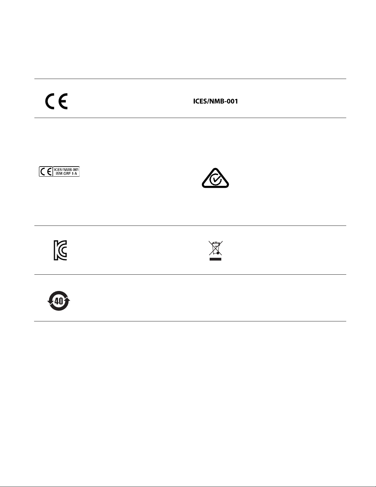
Regulatory Markings
The CE mark is a registered trademark of the
European Community. This CE mark shows that
the product complies with all the relevant
European Legal Directives.
ICES/NMB-001 indicates that this ISM device
complies with the Canadian ICES-001.
Cet appareil ISM est conforme a la norme
NMB-001 du Canada.
The CE mark is a registered trademark of the
European Community. This CE mark shows that
the product complies with all the relevant
European Legal Directives.
ICES/NMB-001 indicates thatthis ISM
device complies with the Canadian ICES-001.
Cet appareil ISM est conforme a la norme
NMB-001 du Canada.
ISM GRP.1 Class A indicates that this is an
Industrial Scientific and Medical Group 1 Class A
product.
The RCM mark is a registered trademark of the
Spectrum Management Agency of Australia. This
signifies compliance with the Australia EMC
Frameworkregulations under the terms of the
Radio Communication Act of 1992
This symbol is a South Korean Class A EMC
Declaration. This is a Class A instrument suitable
for professional use and in electromagnetic
environment outside of the home.
This instrument complies with the WEEE
Directive (2002/96/EC) marking requirement.
This affixed product label indicates that you must
not discard this electrical or electronic product in
domestic household waste.
This symbol indicates the time period during
which no hazardous or toxic substance elements
are expected to leak or deteriorate during normal
use. Forty years is the expected useful life of the
product.

Waste Electrical and Electronic Equipment (WEEE) Directive 2002/ 96/EC
This instrument complies with the WEEE Directive (2002/96/EC) marking requirement. This
affixed product label indicates that you must not discard this electrical or electronic product
in domestic household waste.
Product category
With reference to the equipment types in the WEEE directive Annex 1, this instrument is
classified as a “Monitoring and Control Instrument” product.
The affixed product label is as shown below.
Do not dispose in domestic household waste.
To return this unwanted instrument, contact your nearest Keysight Service Center, or visit
http://about.keysight.com/en/companyinfo/environment/takeback.shtml for more
information.

Sales and Technical Support
To contact Keysight for sales and technical support, refer to the support links on the
following Keysight websites:
–
www.keysight.com/find/rfuw
(product-specific information and support, software and documentation
updates)
–
www.keysight.com/find/assist
(worldwide contact information for repair and service)

Table of Contents
Notices......................................................................................................................................... 2
Copyright Notice ......................................................................................................................... 2
Manual Part Number................................................................................................................... 2
Edition.......................................................................................................................................... 2
Printed in: .................................................................................................................................... 2
Published by:............................................................................................................................... 2
Technology Licenses ................................................................................................................... 2
Declaration of Conformity........................................................................................................... 2
U.S. Government Rights ............................................................................................................. 2
Safety Information....................................................................................................................... 2
Safety Considerations ................................................................................................................. 4
Environmental Conditions........................................................................................................... 5
Regulatory Information ............................................................................................................... 6
Regulatory Markings................................................................................................................... 7
Waste Electrical and Electronic Equipment (WEEE) Directive 2002/ 96/EC............................ 8
Product category......................................................................................................................... 8
Sales and Technical Support...................................................................................................... 9
1 Overview................................................................................................................................. 12
List of Contents in the RF Microwave Kit Hardware ................................................................ 13
X-Microwave System ................................................................................................................ 13
Screw Lengths........................................................................................................................... 14
X-MWblocks.............................................................................................................................. 14
X-MWprotoplate (Top View)..................................................................................................... 15
X-MWprotoplate (Bottom View)............................................................................................... 16
The X-MWcontroller and Power and Raspberry Pi Interface Boards...................................... 17
The X-MWcontroller ................................................................................................................. 17
Power Interface Board .............................................................................................................. 17
Programming Interface Board (Latch Enable (LE) and Control Ribbon Cables)..................... 17
Power Cable .............................................................................................................................. 19
Bias and Control for X-MWblocks............................................................................................ 19
Bias and Control Board Placement .......................................................................................... 20

2 Prototyping Kit Setup............................................................................................................. 21
Wiring between Interface Boards............................................................................................. 21
Procedure .................................................................................................................................. 22
3 Keysight Software Setup ....................................................................................................... 23
System and Installation Requirements..................................................................................... 23
Install PathWave RF Synthesis (Genesys) ................................................................................ 23
Install PathWave Advanced Design System (ADS) .................................................................. 23
Install PathWave EM Design (EMPro) ...................................................................................... 23
Install PathWave System Design (SystemVue) ........................................................................ 24
Install FieldFox Data Link.......................................................................................................... 24
Install PathWave BenchVue (Optional) .................................................................................... 24
4 X-MWcontroller Setup........................................................................................................... 25
Configuring the X-MWcontroller with an HDMI Display ......................................................... 25
Configuring the X-MWcontroller with your Computer as the Display .................................... 26
Configuring the X-MWcontroller using Mac............................................................................ 29
Configuring the X-MWcontroller using Linux .......................................................................... 30
Using the X-MWcontroller Platform......................................................................................... 31
Raspberry Pi Troubleshooting .................................................................................................. 34
Mouse/keyboard attached to the USB port of the X-MWcontroller becomes unresponsive 34
Can't program the devices on my X-MW prototyping plate ................................................... 34
Can't communicate with my X-MWcontroller over VNC......................................................... 34
The RaspberryPi is unresponsive or not functioning properly................................................. 35
Updating the X-MWcontroller Part Library.............................................................................. 36
Recreate PLL_and_DSA_Config.xmdat file .............................................................................. 37
5 X-MWblock Default Positions and Performance Verification............................................... 43
Return Components to their Proper Positions ......................................................................... 43
Measure the Receiver’s Supply Current................................................................................... 44
Measure the Receiver’s Gain .................................................................................................... 45
Measure the Receiver’s Spurious Responses........................................................................... 46
6 Troubleshooting the Signal Path........................................................................................... 47

1 Overview
RF and microwave engineering covers the physical layer of wireless communication and are
incorporated into almost everything that transmits or receives a radio wave, such as mobile
phones, radios and WLAN. The growth of 5G drives rapid innovations in the technology
landscape and imposes new requirements on RF components, resulting in design challenges
such as increased integration and exponential demands on performance. The increasing
complexity brought by 5G means many companies will need additional expertise to execute
the technology in their devices designs.
Keysight’s RF and Microwave Lab Courseware focuses on end-to-end RF system design flow,
and integrates industry-oriented, real-world examples to prepare students for emerging
technology trends. The lab courseware comes with a modular prototype kit utilizing a
1.8 GHz receiver module — a 5G New Radio n3 band — as well as lab sheets and assignments
that focus on the complete physical design spectrum, from specifications and simulation to
prototype building and validation.
The RF and Microwave Lab Courseware forms a core component of the Keysight RF and
Microwave Teaching Solution. In addition to the lab courseware, this comprehensive solution
includes Keysight PathWave Advanced Design System (ADS) and SystemVue software, as
well as hardware instruments such as a network analyzer, RF signal generator and RF
spectrum analyzer.
The RF Microwave Circuit Design, Simulation and Measurement Courseware, 5G NR n3
covers the following:
Courseware Contents
−Modular prototype kit
–RF education hardware kit
–Kit controller
–RF adapters and splitter
–Cables (RF, power, control, BNC)
–Power adapter and carry case
−Editable lab sheets and model answers
−Problem-based assignments
−Covers 50 hours of lab sessions
Keysight U3851A RF Microwave Circuit Design, Simulation and Measurement 13
Courseware, 5G NR n3 Getting Started Guide
List of Contents in the RF Microwave Kit Hardware
Item Quantity
1.
Assembled X-MWprotoplate Kit for Module 1
1
2.
X-MWcontroller RaspberryPi Kit
1
3.
GSG Placement Tool
1
4.
Hex driver for 1-72 socket head cap screws
1
5.
Power adapter 13W Plug In Power Supply 5.1 V, 2.5 A, Micro USB 1
6.
High Performance RF Cable SMAm to SMAm 0.9 m
2
7.
Adaptor, N-type to SMA female
3
8.
Power Splitter SMA 1 GHz to 2.5 GHz
1
9.
SMA-F to SMA-F Thru Coaxial Adapter
1
10.
Carrying Case with inner foam 1
11.
Cable Assembly-Coaxial RG58C/U 50-Ohm BNC-Plug BNC-Plug PVC Black
1
12.
Connector-RF SMA Terminator Plug Straight 50-Ohm 18 GHz-MAX 1
13.
SMA-f to SMA-m 50 mm cable
1
14.
Power supply cable from kit to external power supply 1
15.
Cable Assembly-Coaxial RG-58/U 50-Ohm SMA-Male BNC-Male 1m-LG
1
16.
LAN Crossover Cable, 2.13 m
1
17.
SMA-m to SMA-m 0.5 m RG316 Cable
2
NOTE The LAN crossover cable facilitates direct peer-to-peer LAN device connection such as the
Raspberry Pi to your computer. A regular “straight through” LAN cable may be adequate for
devices that have Auto MDI-X ports that automatically choose the MDI or MDI-X configuration to
properly match the other end of the link. The crossover cable should not be used when
connecting a device to a switch or router.
X-Microwave System
RF Blocks are placed on the top side of the X-MWprotoplate and are connected together launch-to-
launch with the ground-signal-ground (gsg) jumper solderless interconnect. Each gsg jumper is held
down by two anchors, one on each side of the gsg jumper. Bias and Control X-MWblocks contain
spring pins that make a connection to vias on the bottom side of the RF block.
X-MWblock RF X-MWprobe Anchor X-MWblock
Bias and Control X-MWprotoplate gsg Jumper

Keysight U3851A RF Microwave Circuit Design, Simulation and Measurement 14
Courseware, 5G NR n3 Getting Started Guide
Screw Lengths
All screws are 1-72 socket head cap screws made of 18-8 stainless steel. Using the proper length
screws is important so that nothing protrudes through the top or bottom of the prototyping plate.
Screws that are too long can scratch or even break the board below it. (Even a single bag of standard
machine screws can also vary in length due to manufacturing variability.) Screws should not be
overtightened. Finger-tight is adequate for most applications if you do not have a torque wrench. The
torque specification is 7 oz-in / 5 N-cm. If you overtighten the screws, you could damage the
threaded holes in the prototyping plate or PCB surface.
X-MWblocks (bottom of
plate)
1-72 x 1/8”
(0.125”)
X-MWblocks (top)
X-MWprobe (short)
1-72 x 5/32”
(0.156”)
X-MWanchor
Pinbridge
1-72 x 1/4”
(0.25”)
X-MWProbe (tall)
X-MWwall (short)
1-72 x 3/8”
(0.375”)
X-MWblocks
These components are mounted to the X-MWprotoplate. Descriptions may be searched for and
viewed at https://www.xmicrowave.com/.
XM-W Part Number Description Part MFG MRG Part PCB Number Quantity
XM-A6Y2-0204D LTCC Band Pass Filter Mini-Circuits BFCN-1860 29 1
XM-A2L2-0404D Oscillator - 100 MHz PLE SM77D 159 1
XM-A2N1-0409D U-Turn Transmission Line XMW 184 1
XM-B4V6-0604D Double-Double Balance Mixer
Marki
Microwave
T3-06LCQG 191 1
XM-A2M7-0404D Transmission Line - Straight X-MW 306 1
XM-A5M6-0409D PLL-VCO ADI ADF4355-3BCPZ 382 1
XM-A3V3-0404D SAW Filter Centered at 168.5 MHz Qorvo 856512 412 1
XM-B1F3-0404D BAW Filter Centered at 1842.5 GHz Qorvo TQQ0303 473 1
XM-A4H9-0404D General Purpose Amplifier ADI ADL5611 516 1
XM-B5A2-0404D General Purpose Amplifier (5 V) Mini-Circuits Gali-51 530 1
XM-A767-0404D Low Noise Amplifier Qorvo TQL9092 613 1
XM-A3K9-0604D Digital Step Attenuator Peregrine PE43713 701 1
XM-B2A3-0604D Power Amplifier ADI HMC453ST89 802 1
XM-B2B7-0604D Double Balance Mixer (6 GHz) Mini-Circuits SIM-63LH 906 1
XM-B4V4-0420D Microstrip and Coplanar Example X-MW 907 1
XM-B162-0407-SP Voltage Regulator +VIN2 – 5-Volt X-MW 909 3
XM-B161-0407-SP Voltage Regulator +VIN2 - 3.3-Volt X-MW 910 1
XM-B164-0607D-SP Bias Ctrl for PE43713 DSA +VIN2 X-MW 911 1
XM-B165-0709D-SP Bias Ctrl for ADRF-4355-3BCPZ PLL/VCO +VIN2 X-MW 912 1
XM-B1F4-1204D Lumped Low Pass 168.5 MHz + 45 MHz X-MW 976 1
XM-B158-0407-SP Voltage Regulator +VIN1 – 5-Volt X-MW 997 1
XM-B4V5-0604D Double Balance Mixer (500 MHz) Mini-Circuits ADE-1LH 1041 1

Keysight U3851A RF Microwave Circuit Design, Simulation and Measurement 15
Courseware, 5G NR n3 Getting Started Guide
X-MWprotoplate (Top View)
The components on the X-MWprotoplate are labeled in the symbol view (left) and layout view (right)
with the description below.
Table 1. List of items assembled on the X-MWprotoplate (top view).
Item Item
1 Transmission Line Samples 10 Mixer Driver Amplifier
2 LTCC Filter 11 Synthesizer / PLL
3 X-MWprobe 12 Reference Oscillator
4 Driver Amplifier 13 Mixer
5 IF Bandpass Filter (BPF) 14 Transmission Line
6 Mixer 15 Low Noise Amplifier (LNA)
7 Lumped Element LPF 16 RF Bandpass Filter (BPF)
8 Transmission Line 17 Digital Step Attenuator
9 Mixer 18 Power Amplifier

Keysight U3851A RF Microwave Circuit Design, Simulation and Measurement 16
Courseware, 5G NR n3 Getting Started Guide
X-MWprotoplate (Bottom View)
The components on the X-MWprotoplate are labeled in layout view with the description below.
Table 2. List of items assembled on the X-MWprotoplate (bottom view).
Item Item
19 Programming Interface Board (PCB 915) 24
PLL 5-Volt Regulator and Control Powered by VIN2+ (PCB
912)
20 5-Volt Regulator Powered by VIN1+ (PCB 997) 25 Power Interface Board (PCB 914)
21
DSA 5-Volt Regulator and Control Powered by VIN2+
(PCB 911)
25A Power Cable Connection
22 5-Volt Regulator Powered by VIN2+ (PCB 909) 26 5-Volt Regulator Powered by VIN2+ (PCB 909)
23 3.3-Volt Regulator Powered by VIN2+ (PCB 910) 27 5-Volt Regulator Powered by VIN2+ (PCB 909)
NOTE
−
+VIN1 provides power to the Power Amplifier (PA) only.
−+VIN2 provides power to the Receiver, that is all the remaining components.
−-VIN2 is not used and reserved for future use

Keysight U3851A RF Microwave Circuit Design, Simulation and Measurement 17
Courseware, 5G NR n3 Getting Started Guide
The X-MWcontroller and Power and Raspberry Pi Interface Boards
The X-MWcontroller
The X-MWcontroller RaspberryPi is used to program the PLL, DSA and any other
programmable block. It provides a dedicated graphical user interface on an HDMI monitor or
remotely on a computer.
Power Interface Board
The Power Interface board distributes power from the connected power supply to J1 through
J10. +VIN1 is used for a positive supply, capable of supplying +6 V at up to 1 Amp of current.
+VIN2 / -VIN2 is used for a +/- dual voltage supply providing +6 V and -6V at up to 1 amp of
current. (The negative supply is not used; is reserved for future use.)
Programming Interface Board (Latch Enable (LE) and Control Ribbon Cables)
The PLL-VCO and DSA X-Microwave block each require a control board. They are
programmable over SPI (Serial Peripheral Interface) bus, a 3-wire digital protocol. The DATA
line is sampled on each rising edge of the CLOCK shared among all devices. Programming is
enabled on each individual device through Latch Enable (LE) in an “active low” state. Data
and clock lines are ignored when Latch Enable is held “high” and the device is programmed
when Latch Enable is held “low”.
The X-MWcontroller RaspberryPi is connected to the Control Interface board using a 40-pin
to 26-pin cable. The physical Latch Enable port is chosen by connecting the desired
programmable control board to one of the six numbered LE ports (LE0 to LE5). The physical
LE port on the bottom of the prototyping plate should also be selected in the X-MWcontroller
software interface.
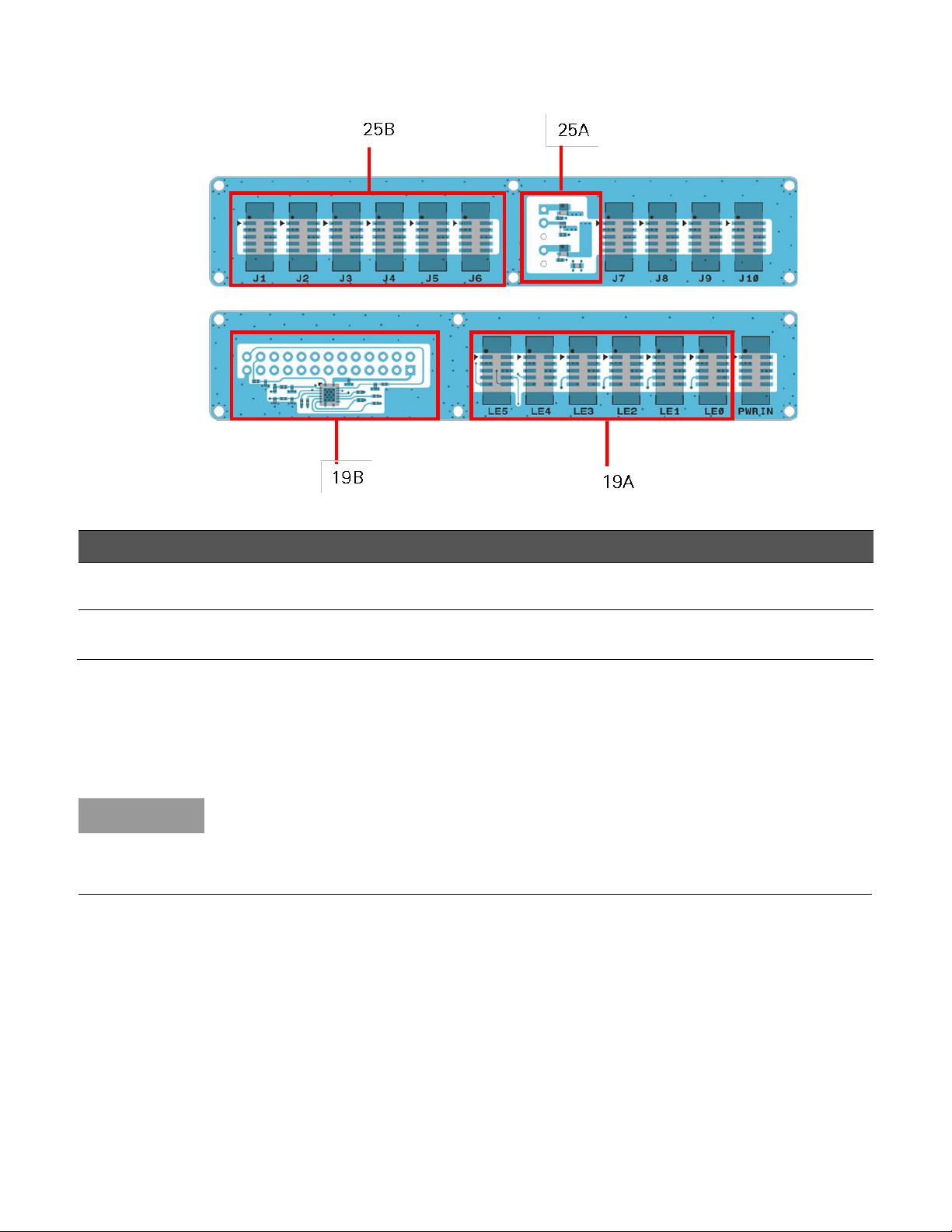
The image below shows the inside view of the Power Interface Board [PCB 0914] and
Raspberry Pi Control Interface Board – Inside View [PCB 0915].
Keysight U3851A RF Microwave Circuit Design, Simulation and Measurement 18
Courseware, 5G NR n3 Getting Started Guide
Table 3. Inside view of the Power and Raspberry Pi Interface Boards.
Item
Item
25B J1 to J10 distribute power to Voltage Regulators 19A LE0 to LE5 distribute power and programming
signals to Control/Voltage Regulators
25A Power from E36312A Power Supply,
+VIN1 (PA) = 6 V, +VIN2 (Receiver) = 6 V 19B 26 Pin Programming Interface to Raspberry Pi
General Purpose Voltage Regulator Boards
a. PCB 0909 = Regulates +6 V In to +5 V Out, +VIN2
b. PCB 0910 = Regulates +6 V In to +3 V Out, +VIN2
c. PCB 0997 = Regulates +6 V In to +5 V Out, +VIN1
NOTE Current Limiting is recommended at the Power Supply:
−+VIN1 powers the PA and its recommended current limit setting is 0.8 A.
−+VIN2 powers the Receiver and its recommended current limit setting is 0.5 A.
−Only energize one supply at a time, never both.

Keysight U3851A RF Microwave Circuit Design, Simulation and Measurement 19
Courseware, 5G NR n3 Getting Started Guide
Power Cable
The diagram below shows the wiring of the power cable:
Bias and Control for X-MWblocks
Each X-MWblock (top side) that requires power will have a corresponding Voltage Regulator or
Control/Regulator board on the bottom side of the X-MWprotoplate. Spring (pogo) pins pass the
signal from regulator and control blocks to vias on the bottom side of RF blocks ●.
10-pin ribbon cables connect each Voltage Regulator to the Power Interface board and each control
board to the Pi Control Interface board.
–Voltage Regulator boards may be connected to any jack (J1 – J10) on the Power Interface
board.
–Control/Regulator boards must be connected as shown below to the Programming Interface
board.

Keysight U3851A RF Microwave Circuit Design, Simulation and Measurement 20
Courseware, 5G NR n3 Getting Started Guide
Bias and Control Board Placement
Matched bias voltage and control boards are placed on the bottom of the prototyping plate supplying
the microwave blocks with the necessary power and control signals. Spring-pins with shielded collets
are soldered to the bias and control circuit board provide a shielded electrical connection through the
prototyping plate to the RF X-MWblock.
Tip: After moving an RF board, hold the prototyping plate up to the light and you can see light
coming through the vias which shows you how you need to align the control board.
Table of contents
Popular Educational Equipment manuals by other brands

TruCorp
TruCorp AirSim user manual

Pitsco Education
Pitsco Education BUILDERSPACES SPACEPORT Assembly instructions

fischertechnik
fischertechnik STEM Coding Pro Assembly instruction

Learning Resources
Learning Resources interactive ELECTRONICS Quizzillion Use and care guide

Regina
Regina BE-306 instruction manual

Rompa
Rompa 20019 manual

IngMar Medical
IngMar Medical Laerdal ASL 5000 Quick setup guide

Prestan
Prestan Adult Manikin 2000 Series Use and care instruction

sparkfun
sparkfun Inventor's Kit manual

Betzold
Betzold 759884 instructions

LEXIBOOK
LEXIBOOK POWERMAN ADVANCE ROB28EN instruction manual

DIVERSIFIED WOODCRAFTS
DIVERSIFIED WOODCRAFTS AUGMENTED REALITY Series manual


