Linear Technology DC164 Quick setup guide
Other Linear Technology Media Converter manuals
Linear Technology
Linear Technology LTC3118EUFD Quick setup guide
Linear Technology
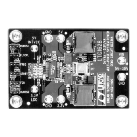
Linear Technology LTC1628 User manual
Linear Technology
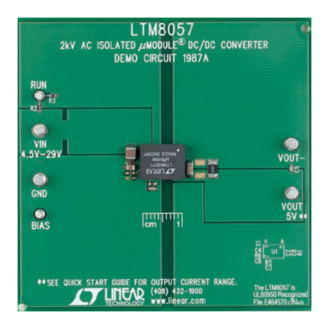
Linear Technology LTM8057 Quick setup guide
Linear Technology
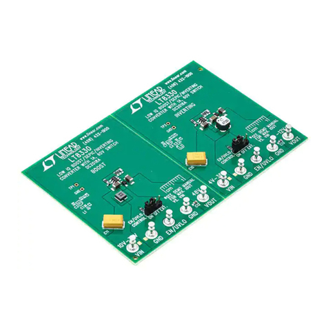
Linear Technology LT8330 User manual
Linear Technology
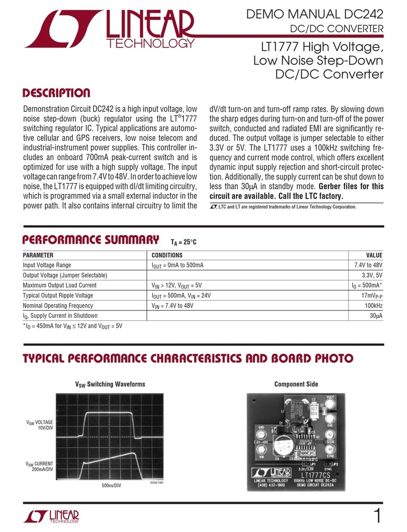
Linear Technology DC242 Quick setup guide
Linear Technology
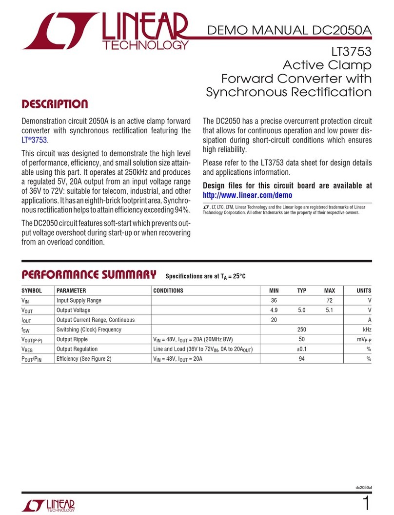
Linear Technology DC2050A User manual
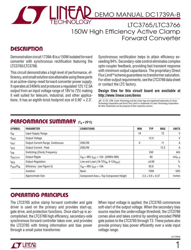
Linear Technology
Linear Technology DC1739A-B Quick setup guide

Linear Technology
Linear Technology LTC3130EUD-1 User manual
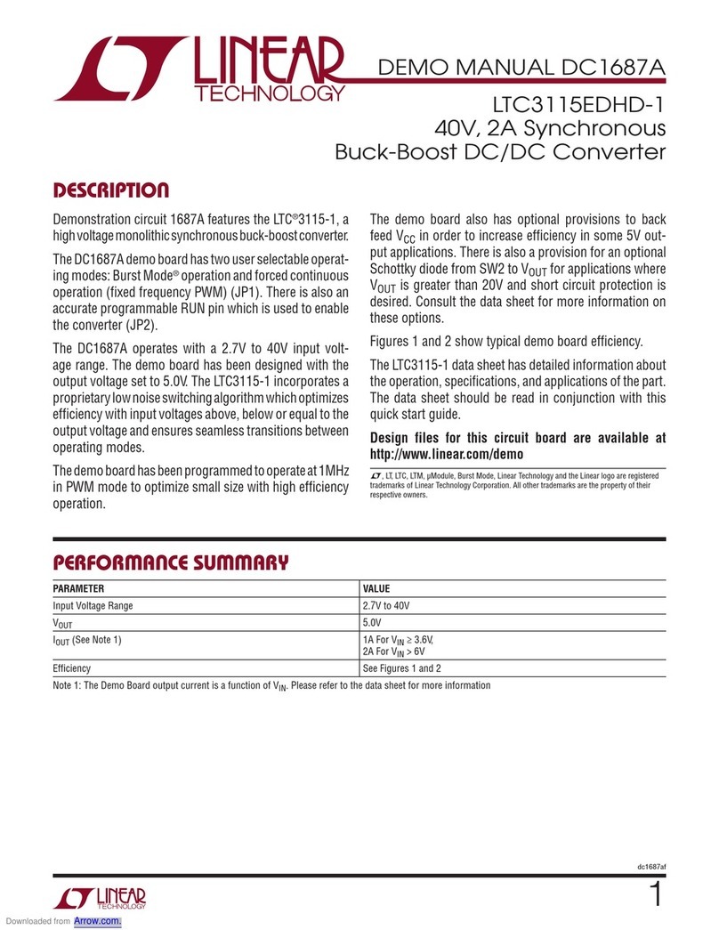
Linear Technology
Linear Technology DC1687A Quick setup guide
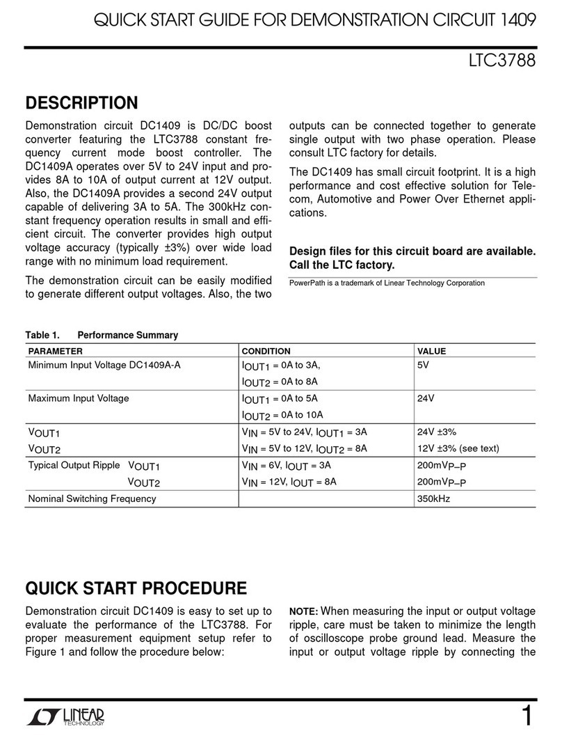
Linear Technology
Linear Technology DC1409 User manual
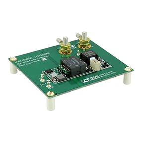
Linear Technology
Linear Technology LTC3725 User manual
Linear Technology
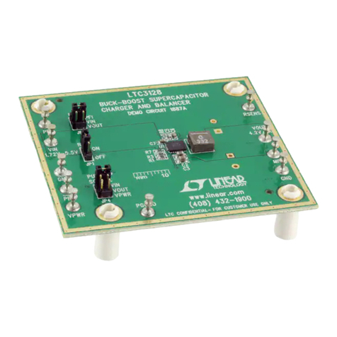
Linear Technology DC1887A Quick setup guide
Linear Technology
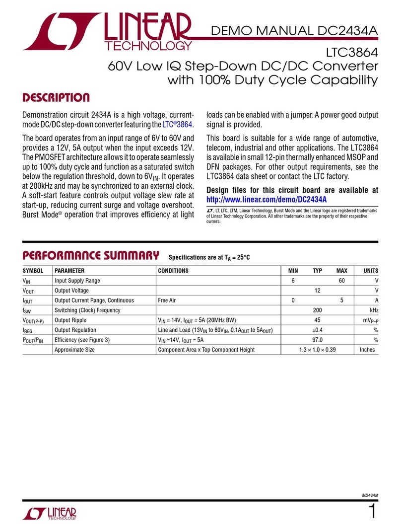
Linear Technology DC2434A Quick setup guide
Linear Technology
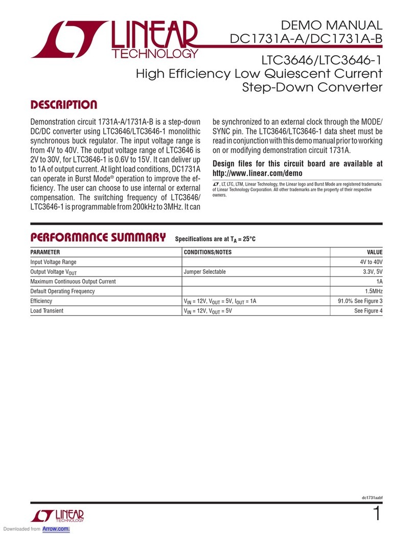
Linear Technology DC1731A-A Quick setup guide
Linear Technology
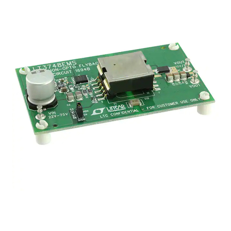
Linear Technology LT3748 Quick setup guide

Linear Technology
Linear Technology DC1929A Quick setup guide
Linear Technology
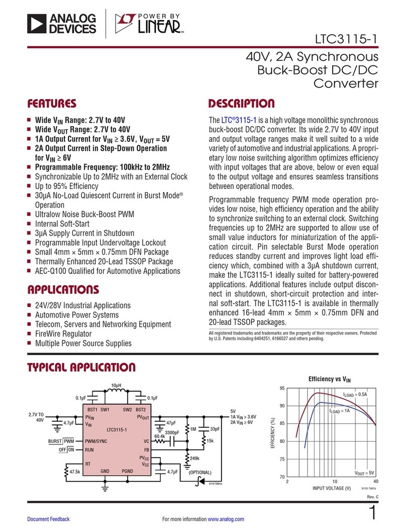
Linear Technology LTC 3115-1 User manual
Linear Technology
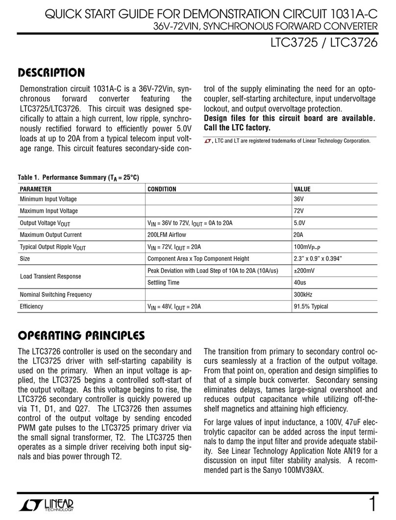
Linear Technology LTC3725 User manual

Linear Technology
Linear Technology LTC3118 User manual
Linear Technology
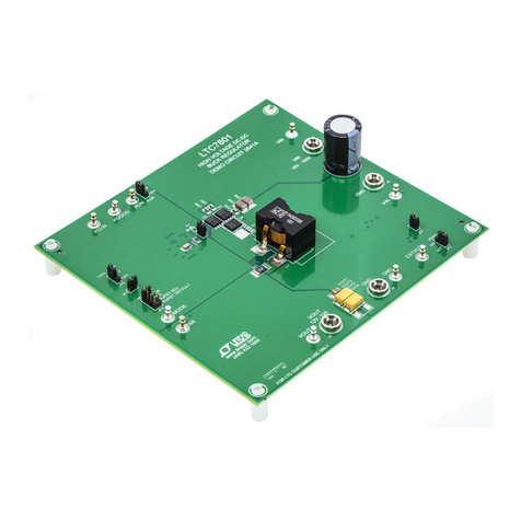
Linear Technology DC2641A Quick setup guide
Popular Media Converter manuals by other brands
H&B
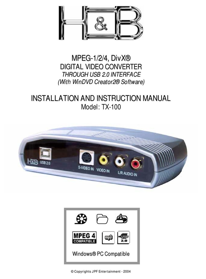
H&B TX-100 Installation and instruction manual
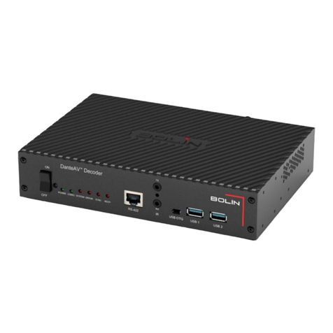
Bolin Technology
Bolin Technology D Series user manual
IFM Electronic
IFM Electronic Efector 400 RN30 Series Device manual

GRASS VALLEY
GRASS VALLEY KUDOSPRO ULC2000 user manual
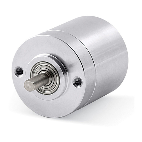
Lika
Lika ROTAPULS I28 Series quick start guide
Weidmuller
Weidmuller IE-MC-VL Series Hardware installation guide
Optical Systems Design
Optical Systems Design OSD2139 Series Operator's manual

Tema Telecomunicazioni
Tema Telecomunicazioni AD615/S product manual
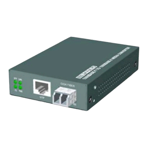
KTI Networks
KTI Networks KGC-352 Series installation guide
Gira
Gira 0588 Series operating instructions
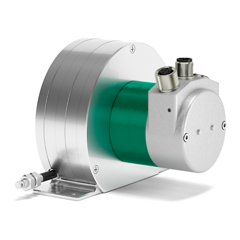
Lika
Lika SFA-5000-FD user guide
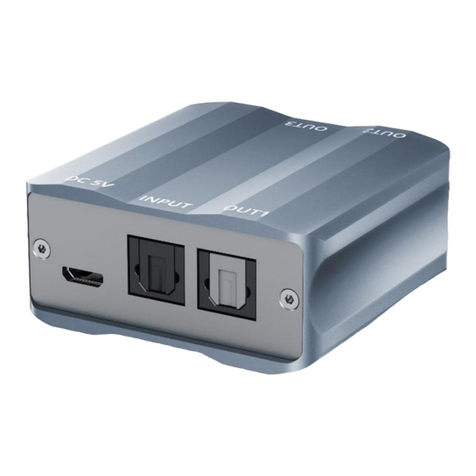
GoMax Electronics
GoMax Electronics SP-2003 user manual
