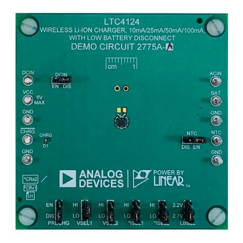
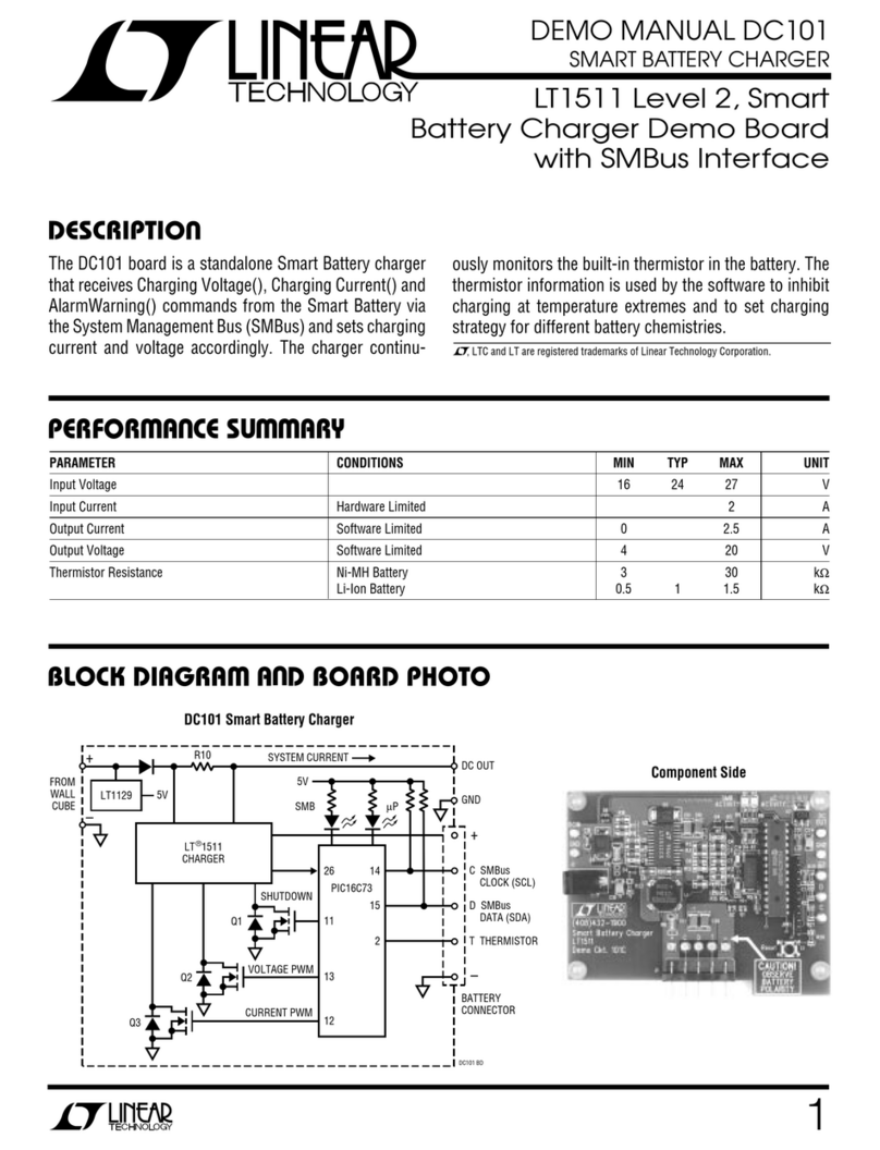
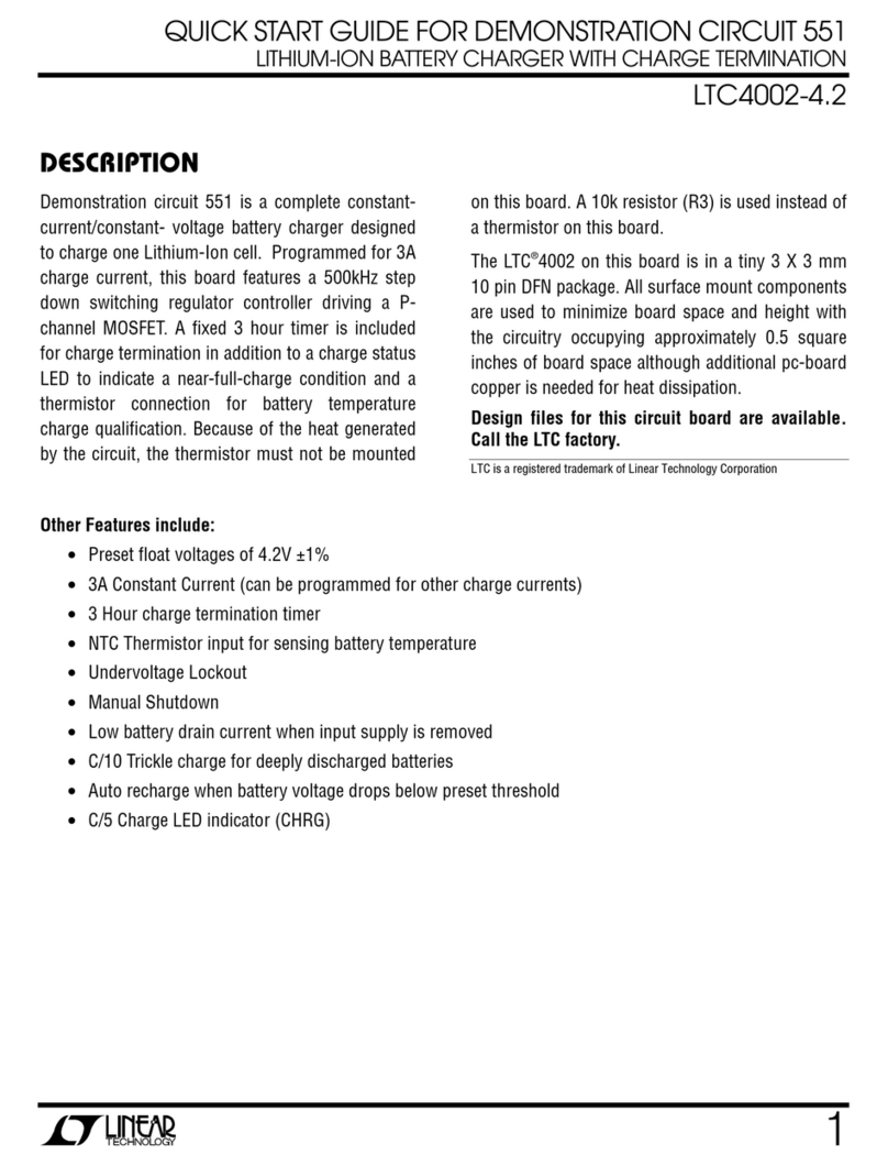
Linear Analog Devices LTC4124 Quick setup guide

1
DEMO MANUAL DC2770A-A-KIT
Rev. 0
DESCRIPTION
LTC4124/LTC4125, 50mA Wireless Li-Ion Charger
Demonstration Kit
DC2770A-A-KIT is a kit of the DC2773A-A transmitter
board (featuring LT C
®
4125) and the DC2775A-C (fea-
turing LTC
®
4124). The DC2775A-C receiver board can
charge a single Li-Ion battery at up to 50 mA with an
air gap of 3.0 mm to 5.0 mm between the transmit and All registered trademarks and trademarks are the property of their respective owners.
PERFORMANCE SUMMARY
CONTENTS
BOARD PHOTO
receive coils. The DC2773A-A transmitter board supports
Foreign Object Detection via the LTC4125.
Design files for this circuit board are available.
Figure1. DC2773A-A Picture Figure2. DC2775A-C Picture
SYMBOL PARAMETER CONDITIONS MIN TYP MAX UNITS
VIN DC2773A-A Voltage Input IVIN ≤ 500mA 4.5 5.5 V
IIN DC2773A-A VIN Current VIN = 5V 500 mA
VBAT DC2775A-C Battery Charge Voltage VSEL1 = HI, VSEL2 = HI 4.35 V
VSEL1 = HI, VSEL2 = LO 4.20 V
VSEL1 = LO, VSEL2 = HI 4.1 V
VSEL1 = LO, VSEL2 = LO 4.00 V
IBAT DC2775A-C Charge Current VBAT = 4.0V, ISEL1 = VCC, ISEL2 = GND 50 mA
AIR-GAP Separation Between LTX and LRX Coils 3 3.5 5 mm
fTX_TANK DC2773A-A Resonant Tank Frequency 200 kHz
fRX_TANK DC2775A-C Resonant Tank Frequency 200 kHz
1 × DC2773A-A (LTC4125) Transmitter Demo Board
1 × DC2775A-C (LTC4124) Receiver Demo Board

2
DEMO MANUAL DC2770A-A-KIT
Rev. 0
QUICK START PROCEDURE
Refer to Figures 3, 4, and 5 for the proper measurement
equipment setup, DC2775A-C mounting on DC2773A-A,
and follow the procedure below:
NOTE:When measuring the input or output voltage ripple,
care must be taken to avoid a long ground lead on the
oscilloscope probe. Measure the input or output voltage
ripple by touching the probe tip directly across the signal
and GND terminals. See Figure6 for proper scope probe
technique.
1. Place the DC2775A-C board atop the DC2773A-A board
by aligning the mounting holes and screws on both
boards. Make sure the air-gap between two coils is at
about 3.5mm.
2. The default battery charge voltage is 4.2V and the
charging current is 50mA. Battery charge voltage,
charge current, pre-charge feature and low battery
disconnect voltage can be programmed by jumpers
on the DC2775A-C board.
3. Connect a voltage source PS1 and a 20 Ohm resis-
tor RBAT1 between the BAT and GND turrets of
DC2775A-C, respectively (Figure4). PS1 and RBAT1
make up the battery emulator. Typical power supplies
cannot sink current. By adding a resistor across the
power supply inputs that draws more current than the
maximum battery charging current, the power supply
only sources current even when the battery charge cur-
rent is at its maximum value.
4. Connect an ammeter AM1 between PS1 and the
DC2775A-C BAT turret. Connect a voltage meter
VM1between DC2775A-C BAT and GND turrets.
5. Connect a power supply (PS2) between DC2773A-A
V
IN
turret and GND turret. DC2773A-A can also be pow-
ered through Micro-USB cable to a 5V power source.
6. Set PS1 = 3.7V, PS2 = 5V and enable both power
supplies simultaneously. The DC2773A-A.D5 green
LED should be turned on, indicating the transmitter
is working properly. Note that current indicators on
DC2773A-A.D6-D13 does not reflect the real input cur-
rent in this version. It simply indicates a valid receiver
is found.
7. The DC2775A-C. D1 should be turned on, indicating
power is delivered to the load. Observe AM1. AM1
should be reading 50mA of charge current into the
battery emulator when the battery charger is in con-
stant current mode. Compare VM1 voltage with battery
charge voltage setting to make sure the battery charger
is in constant current mode.
8. When test is done, turn off PS1 and PS2 simultaneously.
Figure3. DC2770A-A-KIT in Operation

5
DEMO MANUAL DC2770A-A-KIT
Rev. 0
THEORY OF OPERATION
The DC2770A-A-KIT demonstrates operation of a mag-
netically coupled resonant Wireless Power Transfer (WPT)
system. The LTC4125 transmitter provides efficient wire-
less power for the LTC4124 receiver to charge the Li-Ion
battery.
DC2773A-A – Wireless Power Transmitter Board
featuring the LTC4125
The LTC4125 implements an AutoResonant drive of the
series resonant transmit tank composed of the transmit
coil LTX, and the transmit capacitor CTX. The AutoReso-
nant driver uses a zero-crossing detector to determine
the resonant frequency of the tank. All sub-sequent duty
cycles discussed here use the resonant period determined
by the AutoResonant circuitry.
The SW1 and SW2 pins each have a half bridge driver. At
zero current crossing, whichever SWXpin has positive
going current, is set to VIN for a duty cycle determined
by the corresponding PTHXpin. When the SWXpin is set
to VIN, it increases the current flowing in the transmitter
resonant tank. The absolute value of the tank current is
determined by the resonant tank components and also by
the reflected load impedance.
VIN
ILVL
Figure7. AutoResonant LC Tank Voltage and Current Waveforms
with Square Wave Input at less than 50% Duty Cycle
The LTC4125 also features optimum power search algo-
rithm. However, it is not implemented in this demo kit.
To check the operation details of optimum power search,
please refer to DC2770A-B-KIT demo manual.
In this demo kit, a 1V voltage reference ADR510 is placed
between IMON pin and GND. In this way, the exit condition
of the search algorithm is always triggered. As a result,
the duty cycle remains almost constant in the operation,
regardless of the change in load current or air gap dis-
tance. The duty cycle of the two half bridge drivers is
pre-defined by PTHM resistors R4 and R8.
The FB pin is driven by the node forming the junction
of the transmit coil LTX, and the transmit capacitor CTX.
The voltage at this node is proportional to the circulating
current in the transmitter resonant tank.
If the receiver is removed from the transmitter, resonant
tank current will rise significantly. The FB pin captures the
rise of resonant current and terminates both half bridge
drivers. As a result, the transmit power is reduced to
standby mode.
If metal foreign objects are inserted between the trans-
mit coil and the receive coil, the resonant frequency will
increase significantly. The LTC4125 captures the rise of
resonant frequency and reduces the transmit power to
standby mode.
In standby mode, the LTC4125 will look for a valid receiver
every 5s. If a valid receiver is found, the power transfer
is resumed.
The LTC4125 uses an NTC resistor to monitor the tem-
perature of the LTXand shut off the transmit power if
the NTC reports a temperature higher than approximately
42°C. Please see the applications section of the data sheet
for more detailed information.
DC2775A-C – Wireless Power Receiver Board
featuring the LTC4124
The DC2775A-C demo board implements a parallel res-
onant LC circuit that connects the LTC4124 between ACIN
and GND pins. The AC waveform on the resonant circuit is
rectified by the internal wireless power manager circuit to
DC voltage on V
CC
pin. This DC source is then fed into the
internal linear battery charger to charge a Li-Ion battery.
As shown in Figure8, when the LTC4124 receives more
energy than it needs to charge the battery, the wireless
power manager in the IC keeps the input voltage to the
IC ( at VCC Pin) low by shunting the receiver resonant

6
DEMO MANUAL DC2770A-A-KIT
Rev. 0
THEORY OF OPERATION
tank to ground. In this way, the linear charger is highly
efficient as its input is always kept just above the battery
voltage, VBAT.
The LTC4124 includes a full featured CC/CV (Constant
Current/Constant Voltage) linear battery charger with
trickle current pre-charge, safety timer termination, bad
battery detection, temperature qualified safe charging and
automatic recharge. The maximum charge current sup-
ported by DC2775A-C is 50mA and the charge voltage is
programmable by VSELXjumpers.
V
CC
2V/DIV
V
ACIN
2V/DIV
V
BAT
2V/DIV
Figure8. Rectification of AC Input and Regulation of VCC

7
DEMO MANUAL DC2770A-A-KIT
Rev. 0
PARTS LIST
ITEM QTY REFERENCE PART DESCRIPTION MANUFACTURER/PART NUMBER
DC2773A-A: Required Circuit Components
1 3 C1, C2, C3 CAP., 100uF, X5R, 6.3V, 10%, 1206 MURATA, GRM31CR60J107KE39L
2 1 C4 CAP., 0.01uF, X7R, 50V, 10%, 0402 KEMET, C0402C103K5RAC7867
3 1 C5 CAP., 0.01uF, X7R, 25V, 10%, 0402, AEC-Q200 MURATA, GCM155R71E103KA37D
4 1 C6 CAP., 4700pF, X7R, 50V, 10%, 0402 AVX, 04025C472KAT2A
5 1 C7 CAP., 680pF, C0G, 25V, 5%, 0402 KEMET, C0402C681J3GACTU
6 1 C8 CAP., 0.1uF, X7R, 50V, 10%, 0402 AVX, 04025C104KAT2A
7 1 C9 CAP., 0.1uF, X7R, 100V, 10%, 0603 AVX, 06031C104KAT2A
8 1 C10 CAP., 1uF, X5R, 16V, 10%, 0402 AVX, 0402YD105KAT2A
9 2 C11, C12 CAP., 47uF, X5R, 6.3V, 20%, 0805 SAMSUNG, CL21A476MQYNNNE
10 1 CRx1 CAP., 0.068uF, C0G, 50V, 5%, 1206, AEC-Q200 MURATA, GCM31C5C1H683JA16L
11 1 CRx2 CAP., 0.022uF, C0G, 50V, 5%, 1206, AEC-Q200 KEMET, C1206C223J5GACAUTO
12 1 D3 DIODE, SCHOTTKY, 70V, 70mA, 0402/SOD-923F COMCHIP, CDBQR70
13 1 D4 DIODE, SWITCHING, 300V, 250mA, SOD-523 DIODES INC., BAS521-7
14 1 D5 LED, GREEN, WATER CLEAR, 0603 LITE-ON, LTST-C190KGKT
15 1 LTx1 IND., 6.8uH, WIRELESS CHRG. COIL, TX., 10%,
2.5A, 125mOHMS, 20.5mm Dia x 2.6mm H, 1 COIL,
1 LAYER
WURTH ELEKTRONIK, 760308101104
16 1 NTC1 RES., 10k OHMS, 1%, NTC THERMISTOR MURATA, FTN55XH103FD4B
17 1 Q2 IC VREF SHUNT 1V SOT23-3 ANALOG DEVICES, INC., ADR510ARTZ#PBF
18 2 R1, R17 RES., 2.2k OHMS, 5%, 1/16W, 0402, AEC-Q200 VISHAY, CRCW04022K20JNED
19 1 R2 RES., 0.22 OHMS, 1W, 1206, AEC-Q200 WIDE
TERMINAL
PANASONIC, ERJB2BFR22V
20 1 R3 RES., 348 OHMS, 1%, 1/16W, 0402 VISHAY, CRCW0402348RFKED
21 2 R4, R5 RES., 100k OHMS, 1%, 1/16W, 0402, AEC-Q200 VISHAY, CRCW0402100KFKED
22 1 R6 RES., 3.24k OHMS, 1%, 1/10W, 0402 PANASONIC, ERJ2RKF3241X
23 1 R8 RES., 13.3k OHMS, 1%, 1/16W, 0402, AEC-Q200 VISHAY, CRCW040213K3FKED
24 2 R10, R14 RES., 100k OHMS, 1%, 1/10W, 0402, AEC-Q200 PANASONIC, ERJ2RKF1003X
25 1 R12 RES., 102k OHMS, 1%, 1/16W, 0402, AEC-Q200 STACKPOLE ELECTRONICS, INC., RMCF0402FT102K
26 1 R15 RES., 22.1K OHMS, 1%, 1/16W, 0402, THICK FILM,
AEC-Q200
VISHAY, CRCW040222K1FKEDC
27 1 R16 RES., 100k OHMS, 1%, 1/10W, 0603, 350V,
AEC-Q200
ROHM, KTR03EZPF1003
28 1 R18 RES., 10k OHMS, 5%, 1/16W, 0402 YAGEO, RC0402JR-0710KL
29 1 R43 RES., 1 OHM, 5%, 1/10W, 0603, AEC-Q200 PANASONIC, ERJ3GEYJ1R0V
30 1 U1 IC, 5W Wireless Power Transmitter, QFN-20 (4x5),
AutoResonant
ANALOG DEVICES, LTC4125EUFD#PBF
Additional Circuit Components
1 3 C13, C15, C16 CAP., 0.01uF, X7R, 50V, 10%, 0402 KEMET, C0402C103K5RAC7867
2 2 C14, C17 CAP., 1uF, X5R, 16V, 10%, 0402 AVX, 0402YD105KAT2A
3 1 D1 LED, RED, WATER-CLEAR, 0603 LITE-ON, LTST-C193KRKT-5A
4 7 D6-D12 LED, BLUE, WATER CLEAR, 0603 LUMEX, SML-LXFP0603USBCTR
5 1 R41 RES., 2.2k OHMS, 5%, 1/16W, 0402, AEC-Q200 VISHAY, CRCW04022K20JNED

8
DEMO MANUAL DC2770A-A-KIT
Rev. 0
ITEM QTY REFERENCE PART DESCRIPTION MANUFACTURER/PART NUMBER
6 2 R13, R45 RES., 0 OHM, 1/16W, 0402 NIC, NRC04ZOTRF
7 1 R19 RES., 10k OHMS, 5%, 1/16W, 0402 YAGEO, RC0402JR-0710KL
8 2 R20, R33 RES., 430 OHMS, 5%, 1/16W, 0402 YAGEO, RC0402JR-07430RL
9 1 R21 RES., 15.4k OHMS, 1%, 1/16W, 0402, AEC-Q200 KOA SPEER, RK73H1ETTP1542F
10 1 R22 RES., 27.4k OHMS, 1%, 1/16W, 0402, AEC-Q200 VISHAY, CRCW040227K4FKED
11 1 R23 RES., 511k OHMS, 1%, 1/16W, 0402, AEC-Q200 VISHAY, CRCW0402511KFKED
12 7 R24-R30 RES., 75k OHMS, 1%, 1/16W, 0402 VISHAY, CRCW040275K0FKED
13 1 R31 RES., 11.3k OHMS, 1%, 1/16W, 0402, AEC-Q200 VISHAY, CRCW040211K3FKED
14 1 R32 RES., 787k OHMS, 1%, 1/16W, 0402 NIC, NRC04F7873TRF
15 7 R34-R40 RES., 6.2k OHMS, 1%, 1/16W, 0402 YAGEO, RC0402FR-076K2L
16 1 R45 RES., 0 OHM, 1/16W, 0402 ROHM, MCR01MZPJ000
17 2 U2, U3 IC, QUAD COMPARATOR LP 1.221VREF, DFN-16
(5x4)
ANALOG DEVICES, LTC1445CDHD#PBF
Hardware: For Demo Board Only
1 3 E1, E4, E5 TEST POINT, TURRET, 0.094" MTG. HOLE, PCB
0.062" THICK
MILL-MAX, 2501-2-00-80-00-00-07-0
2 2 E2, E3 CONN., BANANA JACK, FEMALE, THT, NON-
INSULATED, SWAGE, 0.218"
KEYSTONE, 575-4
3 1 J1 CONN., MICRO USB-B, RCPT., FEMALE, 5-PIN,
HORZ. R/A SMT
WURTH ELEKTRONIK, 629105136821
4 2 JP1, JP2 CONN., HDR., MALE, 1x3, 2mm, THT, STR, NO
SUBS. ALLOWED
SAMTEC, TMM-103-02-L-S
5 6 MP1, MP2, MP5-MP7,
MP10
STANDOFF, NYLON, SNAP-ON, 0.50" WURTH ELEKTRONIK, 702935000
6 1 NTC ASSEMBLY_1 CONN., JSC COAXIAL SOCKET, RCPT., FEMALE,
SMD, 1PORT, I/O TERM.
MURATA, MM5831-2700RB
7 2 XJP1, XJP3 CONN., SHUNT, FEMALE, 2 POS, 2mm WURTH ELEKTRONIK, 60800213421
DC2775A-C: Required Circuit Components
1 1 C3 CAP., 10uF, X5R, 6.3V, 20%, 0603 MURATA, GRM188R60J106ME47D
2 1 CRx2 CAP., 0.047uF, C0G, 25V, 5%, 0805, AEC-Q200 C0805C473J3GACAUTO
4 1 LRx1 IND., 12.6uH, WIRELESS CHRG. COIL RX Qi, 10%,
1.1A, 340mOHMS, 17mm Dia x 0.8mm H, 1 COIL,
1 LAYER
WURTH ELEKTRONIK, 760308101220
5 1 R2 RES., 0 OHM, 5%, 1/16W, 0402 ROHM, MCR01MZPJ000
6 1 RT1 RES., 100k OHMS, 1%, 0201, NTC THERMISTOR TDK, NTCG064EF104FTBX
Additional Circuit Components
1 1 D1 LED, RED, WATER CLEAR, 0201 KINGBRIGHT, APG0603SEC-E-TT
Hardware: For Demo Board Only
1 10 E1-E10 TEST POINT, TURRET, 0.064" MTG. HOLE, PCB
0.062" THICK
MILL-MAX, 2308-2-00-80-00-00-07-0
2 8 JP1-JP8 CONN., HDR, MALE, 1x3, 2mm, VERT, STR, THT WURTH ELEKTRONIK, 62000311121
3 8 XJP1-XJP8 CONN., SHUNT, FEMALE, 2 POS, 2mm WURTH ELEKTRONIK, 60800213421

9
DEMO MANUAL DC2770A-A-KIT
Rev. 0
SCHEMATIC DIAGRAM
4
4
3
3
2
2
1
1
4 4
3 3
2 2
1 1
UNLESS NOTED:
RESISTORS: OHMS, 0402, 1%, 1/16W
CAPACITORS: uF, 0402, 10%, 50V
4.75 - 5.25V
STATUS
DIS
EN
EN
OPT
0.5A
OPT
REVISION HISTORY
ECO DESCRIPTIONREV DATEAPPROVED
-PRODUCTION 06-11-19
WL
VSUP
VSUP
GND
GND
GND
*
*
*
*
*
*
*
SEE TABLE
*
*
*
*
**
01
DNP
037.4k
0.01uF 0.22 ohms ADR510ARTZ
Q2
R14
C5 Q1
0.047 ohms
DNP100k13.3k
R15
R3
22.1k
R44
0
R46
R13 R45
348 DNP
PMBT3904M,316
DNP0 DNP
R2
0.68uF
R8
1.33k
VERSION TABLE
*
100mA-B
SKU#
50mA-A
Charge Current
DNP20k 0
0
VIN
IMON
DATE:
IC NO.
SHEET OF
TITLE: DEMO CIRCUIT SCHEMATIC,
APPROVALS
PCB DES.
APP ENG.
CUSTOMER NOTICE
ANALOG DEVICES HAS MADE A BEST EFFORT TO DESIGN A
CIRCUIT THAT MEETS CUSTOMER-SUPPLIED SPECIFICATIONS;
HOWEVER, IT REMAINS THE CUSTOMER'S RESPONSIBILITY TO
VERIFY PROPER AND RELIABLE OPERATION IN THE ACTUAL
APPLICATION. COMPONENT SUBSTITUTION AND PRINTED
CIRCUIT BOARD LAYOUT MAY SIGNIFICANTLY AFFECT CIRCUIT
PERFORMANCE OR RELIABILITY. CONTACT LINEAR
TECHNOLOGY APPLICATIONS ENGINEERING FOR ASSISTANCE.
THIS CIRCUIT IS PROPRIETARY TO ANALO DEVICES AND
SUPPLIED FOR USE WITH ANALOG DEVICE PARTS.
SCALE = NONESIZE:
SKU NO. SCHEMATIC NO. AND REVISION:
PCA BOM:
PCA ASS'Y:
TM
DEVICES
Milpitas, CA 95035
Fax: (408)434-0507
www.analog.com
Phone: (408)432-1900
ANALOG
1630 McCarthy Blvd.
AHEAD OF WHAT'S POSSIBLE
12
NC
LTC4125
50mA/100mA AUTORESONANT WIRELESS TRANSMITTER
700-DC2773A_REV02
710-DC2773A_REV01
705-DC2773A_REV01
N/A
06-11-19
WL
C5
R5
100k
C6
4700pF
D4
BAS521-7
R46
R43
1
C12
47uF
0805
R1
2.2k
D1
RED
E2
JP1
13
2
U1 LTC4125-UFD
IN
1
16
GND
21
PGND
IN1
20
IN2
17
SW1 19
SW2 18
IS-
3IS+
4
FB
13 NTC
6
IIMON
5
CTS
2
EN
15
CTD
14
STAT 8
PTHM
12
PTH1
11
PTH2
10
DTH
7
FTH
9
LTx1
6.8uH
760308101104
E5
D2
BAT54LP
C2
100uF
1206
C10
1uF
T
JSC connector
NTC1
R13
R16
100k
0603
R3
R11
OPT
R45
R12
102k
J1
MICRO USB-B
VBUS 1
D- 2
D+ 3
ID 4
GND 5
GND
8
GND
9GND 7
GND 6
R9
OPT
R15
Q1
PMBT3904M,315
1
32
R6
3.24k
R4
100k
E3
C11
47uF
0805
D5
GREEN
R42
1
R7
OPT
E4
TP1
C4
0.01uF
CRx2
0.022uF 1206
R10
100k
R17
2.2k
C3
100uF
1206
TP2
R8
C9
0.1uF
0603
100V
X7R
C8
0.1uF
C1
100uF
1206
E1
D3
CDBQR70
R14
CRx1
0.068uF 1206
Q2
ADR510ARTZ
2
1
TP3
R2
C7
680pF
R44
R18
10k

10
DEMO MANUAL DC2770A-A-KIT
Rev. 0
SCHEMATIC DIAGRAM
4
4
3
3
2
2
1
1
4 4
3 3
2 2
1 1
INPUT CURRENT
1.221V
DIS
MONITOR
U3.3
U2.3
1.186V
1.186V
EN
PCA ADDITIONAL PARTS
BAR GRAPH FOR AUTORESONANT WIRELESS TRANSMITTER
*
SEE TABLE
150%
100%
85%
71%
57%
43%
29%
14%
IMON
VIN
DATE:
IC NO.
SHEET OF
TITLE: DEMO CIRCUIT SCHEMATIC,
APPROVALS
PCB DES.
APP ENG.
CUSTOMER NOTICE
ANALOG DEVICES HAS MADE A BEST EFFORT TO DESIGN A
CIRCUIT THAT MEETS CUSTOMER-SUPPLIED SPECIFICATIONS;
HOWEVER, IT REMAINS THE CUSTOMER'S RESPONSIBILITY TO
VERIFY PROPER AND RELIABLE OPERATION IN THE ACTUAL
APPLICATION. COMPONENT SUBSTITUTION AND PRINTED
CIRCUIT BOARD LAYOUT MAY SIGNIFICANTLY AFFECT CIRCUIT
PERFORMANCE OR RELIABILITY. CONTACT LINEAR
TECHNOLOGY APPLICATIONS ENGINEERING FOR ASSISTANCE.
THIS CIRCUIT IS PROPRIETARY TO ANALO DEVICES AND
SUPPLIED FOR USE WITH ANALOG DEVICE PARTS.
SCALE = NONESIZE:
SKU NO. SCHEMATIC NO. AND REVISION:
PCA BOM:
PCA ASS'Y:
TM
DEVICES
Milpitas, CA 95035
Fax: (408)434-0507
www.analog.com
Phone: (408)432-1900
ANALOG
1630 McCarthy Blvd.
AHEAD OF WHAT'S POSSIBLE
22
NC
LTC4125
700-DC2773A_REV02
710-DC2773A_REV01
705-DC2773A_REV01
N/A
06-11-19
WL
R38
6.2k
MP2 STANDOFF,NYLON,SNAP-ON,0.50"
R30
75k
U2D
LTC1445-DHD
13
12
14 9
15
3
17
R28
75k
U3B
LTC1445-DHD
7
6
14 9
1
3
17
R40
6.2k
R26
75k
MP6 STANDOFF,NYLON,SNAP-ON,0.50"
R24
75k
U3E
LTC1445-DHD
8
REF
9
V-
D12
BLUE
U3C
LTC1445-DHD
11
10
14 9
16
3
17
MP10 STANDOFF,NYLON,SNAP-ON,0.50"
D10
BLUE
R41
2.2k
R33
430
C15
0.01uF
JP2
1 3
2
D8
BLUE
R35
6.2k
D6
BLUE
NTC_ASSEMBLY_1 RES.,10k OHMS,1%,NTC THERMISTOR
R22
27.4k
U3D
LTC1445-DHD
13
12
14 9
15
3
17
R37
6.2k
R21
15.4k
U2A
LTC1445-DHD
5
4
14 9
2
3
17
D13
OPT
R31
11.3k
R39
6.2k
R29
75k
R20
430
R27
75k
C14
1uF
MP5 STANDOFF,NYLON,SNAP-ON,0.50"
R25
75k
MP1 STANDOFF,NYLON,SNAP-ON,0.50"
U2B
LTC1445-DHD
7
6
14 9
1
3
17
R32
787k
MP7 STANDOFF,NYLON,SNAP-ON,0.50"
R19
10k
C13
0.01uF
D11
BLUE
R23
511k
TAPE,3/4" x 36yds,DOUBLE SIDED POLYIMIDE KAPTON
D9
BLUE
U2E
LTC1445-DHD
8
REF
9
V-
C17
1uF
C16
0.01uF
U2C
LTC1445-DHD
11
10
14 9
16
3
17
EPOXY ADHESIVE,HEAT CURE THERMAL,GREY,30cc SYRINGE
LB1 LABEL
PCB1 PCB, DC2773A REV01
U3A
LTC1445-DHD
5
4
14 9
2
3
17
R34
6.2k
D7
BLUE
R36
6.2k
STNCL1 TOOL, STENCIL, 700-DC2773A REV01

11
DEMO MANUAL DC2770A-A-KIT
Rev. 0
Information furnished by Analog Devices is believed to be accurate and reliable. However, no responsibility is assumed by Analog
Devices for its use, nor for any infringements of patents or other rights of third parties that may result from its use. Specifications
subject to change without notice. No license is granted by implication or otherwise under any patent or patent rights of Analog Devices.
SCHEMATIC DIAGRAM
VCC
ACIN
GND
GND
DCIN
BAT
REVISION HISTORY
ECO REV DESCRIPTION APPROVED DATE
-2PRODUCTION
PCA ADDITIONAL PARTS
UNLESS NOTED:
RESISTORS: OHMS, 0402, 1%, 1/16W
CAPACITORS: uF, 0201, 10%, 50V
OPT
6V MAX
NTC
-B
SKU#
*
-A
13uH
LRx1
7.2uH
CRx1
0.047uF
10mA
25mA
CHARGE CURRENT
CHRG
GND
GND
VERSION TABLE
SEE TABLE
*
HI
LO
HI HI
LO LO
CHRG
EN
DIS
EN
DIS
3.2V
2.7V
LBSEL
ISEL2
VSEL1
DIS
EN
NTC
VSEL1 VSEL2 CHARGE VOLTAGE
HI HI
HI LO
LO
LO
LO
HI
4.35V
4.20V
4.10V
4.00V
PRECHG
0201
VSEL2
0402
-C
-D
50mA
100mA
12.6uH
12.6uH
0.047uF
WIRELESS Li-ION CHARGER, 10mA / 25mA / 50mA / 100mA,
WITH LOW BATTERY DISCONNECT
HI
LO
ISEL1
HI HI
**
**
DCIN
CRx2
CHECK VERSION TABLE
*
3300pF
OPT
OPT
OPT
*
0805
X7R C0G
OPT
C3
OPT
2.2uF
10uF
WL
*
0.047uF
ISEL2
HI
LO
LO
LO
HI
LO
ISEL1
47uF
06-11-19
VCC VCC VCC VCC VCC
VCC
VCC
VCC
DATE:
IC NO.
SHEET OF
TITLE: DEMO CIRCUIT SCHEMATIC,
APPROVALS
PCB DES.
APP ENG.
CUSTOMER NOTICE
ANALOG DEVICES HAS MADE A BEST EFFORT TO DESIGN A
CIRCUIT THAT MEETS CUSTOMER-SUPPLIED SPECIFICATIONS;
HOWEVER, IT REMAINS THE CUSTOMER'S RESPONSIBILITY TO
VERIFY PROPER AND RELIABLE OPERATION IN THE ACTUAL
APPLICATION. COMPONENT SUBSTITUTION AND PRINTED
CIRCUIT BOARD LAYOUT MAY SIGNIFICANTLY AFFECT CIRCUIT
PERFORMANCE OR RELIABILITY. CONTACT LINEAR
TECHNOLOGY APPLICATIONS ENGINEERING FOR ASSISTANCE.
THIS CIRCUIT IS PROPRIETARY TO ANALO DEVICES AND
SUPPLIED FOR USE WITH ANALOG DEVICE PARTS.
SCALE = NONESIZE:
SKU NO. SCHEMATIC NO. AND REVISION:
PCA BOM:
PCA ASS'Y:
TM
DEVICES
Milpitas, CA 95035
Fax: (408)434-0507
www.analog.com
Phone: (408)432-1900
ANALOG
1630 McCarthy Blvd.
AHEAD OF WHAT'S POSSIBLE
11
NC
LTC4124
700-DC2775A_REV02
710-DC2775A_REV02
705-DC2775A_REV02
N/A
06-11-19
WL
E4
D1
RED
JP3
LB1 LABEL
E9
E10
E3
LRx1
E2
U1
LTC4124-LQFN
ACIN
11
GND 13
VSEL2
5
DCIN
12
PRECHG
3
LBSEL
8
BAT
10
CHRG 2
VCC 1
NTC
9
VSEL1
4
ISEL1
6
ISEL2
7
E1
E5
JP5
JP8
JP7
STNCL1 TOOL, STENCIL, 700-DC2775A REV02
E7
CRx1
JP6
CRx2
JP1
PCB1 PCB, DC2775A REV02
E6
R1
0
OPT
C3
0603
E8
Z1
MMSZ5226B
C2
1uF
OPT
RT1
100k JP4
R2
0
JP2

12
DEMO MANUAL DC2770A-A-KIT
Rev. 0
ANALOG DEVICES, INC. 2019
10/19
www.analog.com
ESD Caution
ESD (electrostatic discharge) sensitive device. Charged devices and circuit boards can discharge without detection. Although this product features patented or proprietary protection
circuitry, damage may occur on devices subjected to high energy ESD. Therefore, proper ESD precautions should be taken to avoid performance degradation or loss of functionality.
Legal Terms and Conditions
By using the evaluation board discussed herein (together with any tools, components documentation or support materials, the “Evaluation Board”), you are agreeing to be bound by the terms and
conditions set forth below (“Agreement”) unless you have purchased the Evaluation Board, in which case the Analog Devices Standard Terms and Conditions of Sale shall govern. Do not use the Evaluation
Board until you have read and agreed to the Agreement. Your use of the Evaluation Board shall signify your acceptance of the Agreement. This Agreement is made by and between you (“Customer”)
and Analog Devices, Inc. (“ADI”), with its principal place of business at One Technology Way, Norwood, MA 02062, USA. Subject to the terms and conditions of the Agreement, ADI hereby grants to
Customer a free, limited, personal, temporary, non-exclusive, non-sublicensable, non-transferable license to use the Evaluation Board FOR EVALUATION PURPOSES ONLY. Customer understands and
agrees that the Evaluation Board is provided for the sole and exclusive purpose referenced above, and agrees not to use the Evaluation Board for any other purpose. Furthermore, the license granted
is expressly made subject to the following additional limitations:Customer shall not (i) rent, lease, display, sell, transfer, assign, sublicense, or distribute the Evaluation Board;and (ii) permit any Third
Party to access the Evaluation Board. As used herein, the term “Third Party”includes any entity other than ADI, Customer, their employees, affiliates and in-house consultants. The Evaluation Board is
NOT sold to Customer;all rights not expressly granted herein, including ownership of the Evaluation Board, are reserved by ADI. CONFIDENTIALITY. This Agreement and the Evaluation Board shall all
be considered the confidential and proprietary information of ADI. Customer may not disclose or transfer any portion of the Evaluation Board to any other party for any reason. Upon discontinuation of
use of the Evaluation Board or termination of this Agreement, Customer agrees to promptly return the Evaluation Board to ADI. ADDITIONAL RESTRICTIONS. Customer may not disassemble, decompile
or reverse engineer chips on the Evaluation Board. Customer shall inform ADI of any occurred damages or any modifications or alterations it makes to the Evaluation Board, including but not limited
to soldering or any other activity that affects the material content of the Evaluation Board. Modifications to the Evaluation Board must comply with applicable law, including but not limited to the RoHS
Directive. TERMINATION. ADI may terminate this Agreement at any time upon giving written notice to Customer. Customer agrees to return to ADI the Evaluation Board at that time. LIMITATION OF
LIABILITY. THE EVALUATION BOARD PROVIDED HEREUNDER IS PROVIDED “AS IS”AND ADI MAKES NO WARRANTIES OR REPRESENTATIONS OF ANY KIND WITH RESPECT TO IT. ADI SPECIFICALLY
DISCLAIMS ANY REPRESENTATIONS, ENDORSEMENTS, GUARANTEES, OR WARRANTIES, EXPRESS OR IMPLIED, RELATED TO THE EVALUATION BOARD INCLUDING, BUT NOT LIMITED TO, THE
IMPLIED WARRANTY OF MERCHANTABILITY, TITLE, FITNESS FOR A PARTICULAR PURPOSE OR NONINFRINGEMENT OF INTELLECTUAL PROPERTY RIGHTS. IN NO EVENT WILL ADI AND ITS
LICENSORS BE LIABLE FOR ANY INCIDENTAL, SPECIAL, INDIRECT, OR CONSEQUENTIAL DAMAGES RESULTING FROM CUSTOMER’S POSSESSION OR USE OF THE EVALUATION BOARD, INCLUDING
BUT NOT LIMITED TO LOST PROFITS, DELAY COSTS, LABOR COSTS OR LOSS OF GOODWILL. ADI’S TOTAL LIABILITY FROM ANY AND ALL CAUSES SHALL BE LIMITED TO THE AMOUNT OF ONE
HUNDRED US DOLLARS ($100.00). EXPORT. Customer agrees that it will not directly or indirectly export the Evaluation Board to another country, and that it will comply with all applicable United States
federal laws and regulations relating to exports. GOVERNING LAW. This Agreement shall be governed by and construed in accordance with the substantive laws of the Commonwealth of Massachusetts
(excluding conflict of law rules). Any legal action regarding this Agreement will be heard in the state or federal courts having jurisdiction in Suffolk County, Massachusetts, and Customer hereby submits
to the personal jurisdiction and venue of such courts. The United Nations Convention on Contracts for the International Sale of Goods shall not apply to this Agreement and is expressly disclaimed.
This manual suits for next models
1
Table of contents
Other Linear Batteries Charger manuals
Popular Batteries Charger manuals by other brands
Jamara
Jamara X-Peak 80 BAL V2 Instruction
Panasonic
Panasonic EY0L81 operating instructions

Victor Engineering
Victor Engineering Super-IQ user manual
Piusi
Piusi SELF SERVICE 100 FM Installation, use and maintenance
Midtronics
Midtronics GR1-120 instruction manual
MERLIN SOLAR
MERLIN SOLAR TRAVELPRO 30 user manual


