AB217 LUXEON HR30 Application Brief 20160504 ©2016 Lumileds Holding B.V. All rights reserved. 5
2.2 Surface Finishing
Lumileds recommends using a high temperature organic solderability preservative (OSP) or electroless nickel immersion
gold (ENIG) plating on the exposed copper pads.
2.3 Minimum Spacing
Lumileds recommends a minimum edge to edge spacing between LUXEON emitters of 0.5 mm. Placing multiple LUXEON
emitters too close to each other may adversely impact the ability of the PCB to dissipate the heat from the emitters.
2.4 PCB Substrate Selection and Design
Table 1 provides a summary of various relevant performance characteristics of common PCB substrates to aid material
selection. Specic PCB design considerations for each substrate material are summarized below.
Table 1: General PCB substrate characteristics for consideration when designing a PCB for LUXEON HR30 emitter.
FR-4/CEM-3 MCPCB
Cost Low to medium Medium
PCB thermal conductivity performance Low to high (FR4 with lled and capped
vias but with increase cost) High
LED assembly packing density (thermal
resistance consideration)
Generally suitable for low density
application with a large spacing between
LEDs and/or low operating currents
Suitable for high density application with
close spacing between emitters
Dielectric withstand voltage (top copper
to bottom of substrate) Extremely high (>20kV/mm)
Depends on dielectric material thickness
and its property. Typically 4kV for 100um
thick.
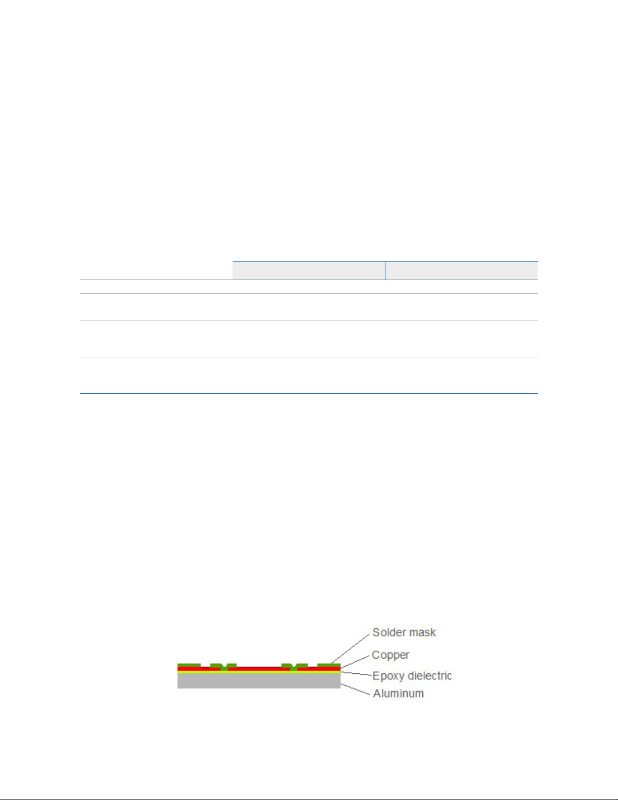
Metal Core PCB
The most common MCPCB construction consists of the following layers (Figure 4):
• A metal substrate, typically aluminum.
• Epoxy dielectric layer. This is the most important layer in the MCPCB construction as it aects the thermal
performance and electrical breakdown strength. The typical thermal conductivity of the dielectric layer on a MCPCB
is around 2Wm-1K-1. A higher value is better for good thermal performance. A thinner dielectric layer is better for
thermal performance but can negatively impact the ability of the MCPCB to withstand electrical insulation test to meet
minimum electrical safety standards as required in certain lighting markets. The typical dielectric thickness layer is
about 100µm.
• Top copper layer. A thicker copper layer improves heat spreading into the PCB but may pose challenges for PCB
manufacturers when fabricating narrow traces or spaces. A thickness of 1oz (35µm) or 2oz (70µm) is common. For
optimum thermal performance on both 1oz and 2oz copper design, the copper area should extend at least 4mm
away from the package outline.
• Use of white solder mask.
Figure 4. MCPCB typical cross section of the three-pad openings with aluminum substrate.