LUMILEDS LUXEON Neo User manual

AUTOMOTIVE
AB172 LUXEON Neo 0.5mm2Application Brief ©2018 Lumileds Holding B.V. All rights reserved.
LUXEON Neo 0.5mm2
Assembly and Handling Information
Introduction
This application brief addresses the recommended assembly and handling
procedures for LUXEON Neo emitters. LUXEON Neo emitters are designed to deliver
high luminous ux and ecacy in automotive exterior lighting applications. Due to the
small size and construction, they require special assembly and handling precautions.
Proper assembly, handling and thermal management, as outlined in this application
brief, ensures high optical output, long term lumen maintenance and high reliability
of LUXEON Neo emitters in automotive applications.
Scope
The assembly and handling guidelines in this application brief apply to LUXEON Neo
0.5mm2products.
Any assembly or handling requirements that are specic to a subset of LUXEON Neo
products is clearly marked. In the remainder of this document, the term LUXEON
Neo refers to any product in the LUXEON Neo product family.

AB172 LUXEON Neo 0.5mm2Application Brief 20180513 ©2018 Lumileds Holding B.V. All rights reserved. 2
Table of Contents
Introduction ...........................................................................1
Scope.................................................................................1
1. Component ........................................................................3
1.1 Reference Document .................................................................3
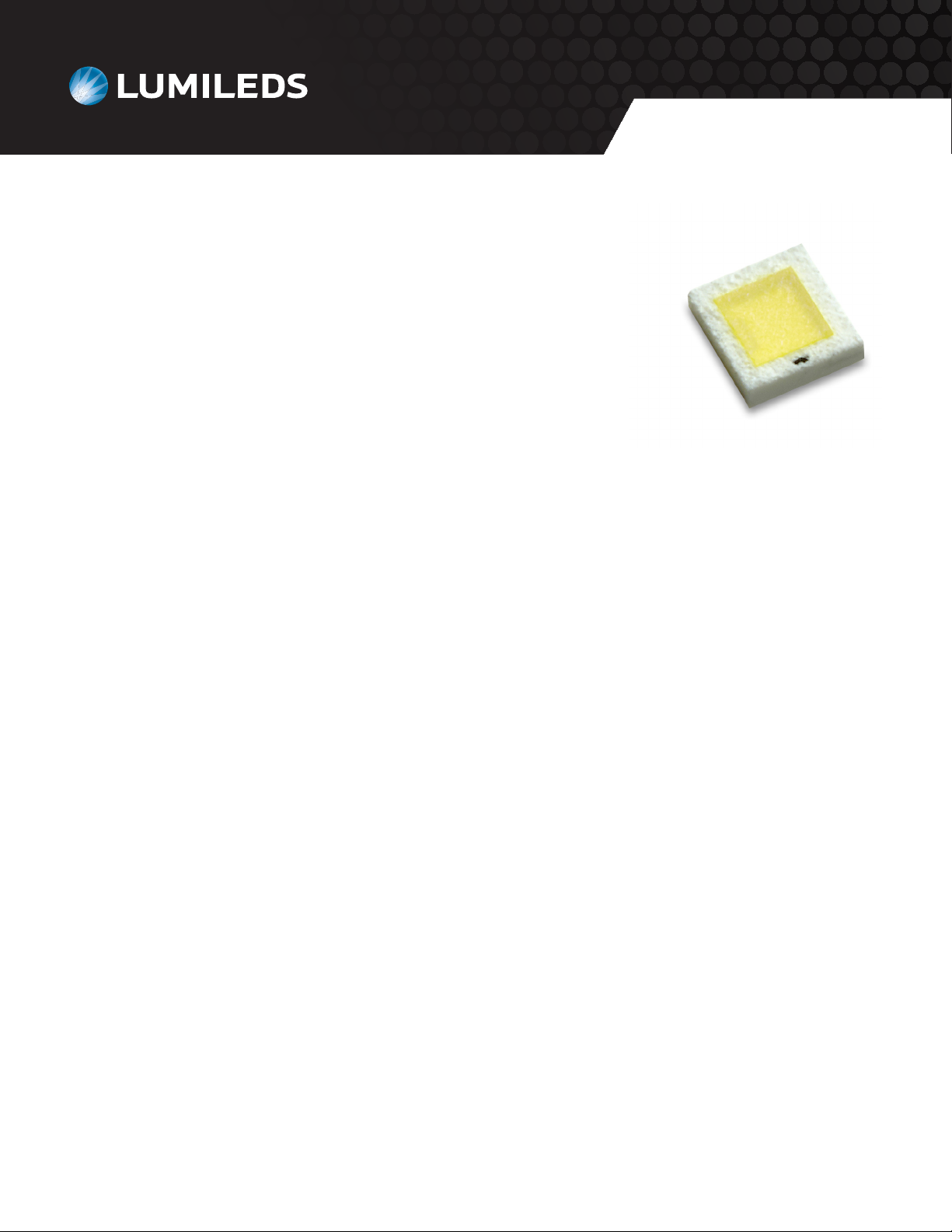
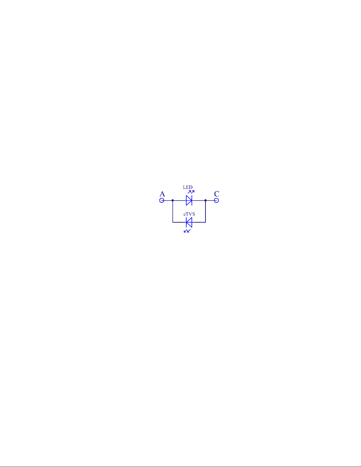
1.2 Description ..........................................................................3
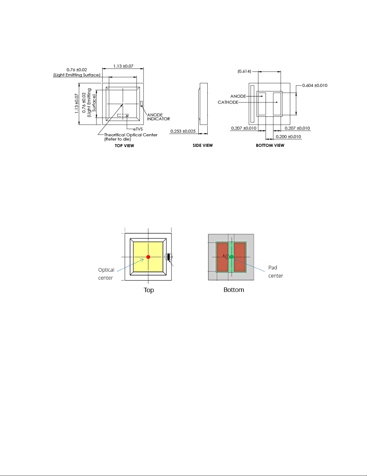
1.3 Form Factor .........................................................................4
1.4 Optical Center .......................................................................4
1.5 Polarity Marking......................................................................5
1.6 Side Coat Geometry ..................................................................5
1.7 Mechanical Files......................................................................6
2. Handling Precautions ................................................................6
2.1 Electrostatic Discharge Protection (ESD).................................................6
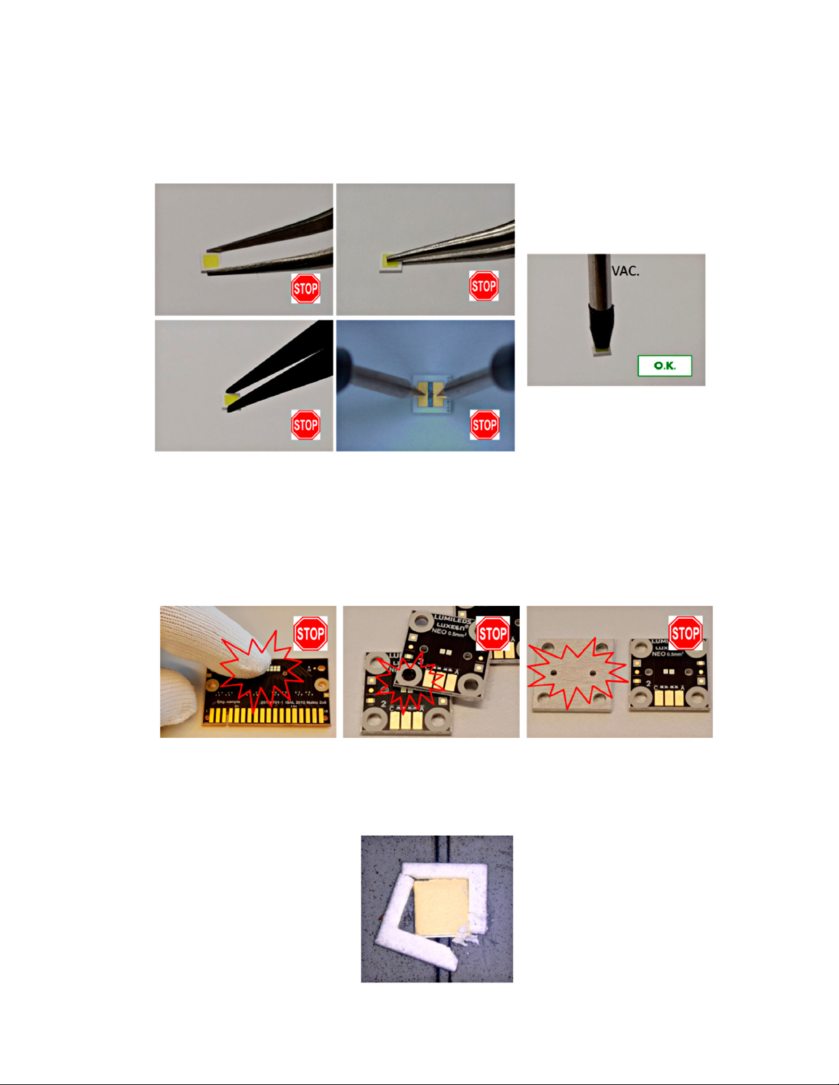
2.2 Component Handling .................................................................6
2.3 Cleaning ............................................................................8
3. Printed Circuit Board ................................................................8
3.1 PCB Requirements ...................................................................8
3.2 Footprint and Land Pattern............................................................8
3.3 Board Fiducial for Solder Mask Dened Footprint ........................................9
3.4 Array Conguration..................................................................10
3.5 Surface Finishing ....................................................................10
3.6 Solder Mask ........................................................................10
3.7 Silk Screen or Ink Printing ............................................................10
3.8 PCB Quality and Supplier.............................................................10
4. Thermal Management ..............................................................11
4.1 Thermal Resistance..................................................................11
4.2 Close-Proximity Thermal Performance .................................................13
4.3 Thermal Measurement Instructions ...................................................13
5. Assembly Process Recommendations and Parameters ..................................15
5.1 Solder Paste ........................................................................15
5.2 Stencil Design.......................................................................15
5.3 Stencil Printing......................................................................16
5.4 Pick and Place Nozzle ................................................................17
5.5 Placement Force/Height Control ......................................................18
5.6 Feed System........................................................................19
5.7 Vision Recognition...................................................................19
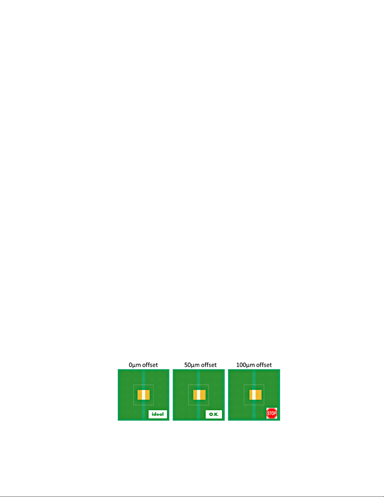
5.8 Placement Accuracy .................................................................20
5.9 Reow Prole .......................................................................20
5.10 Void Inspection ....................................................................21
5.11 Reow Accuracy ...................................................................22
5.12 Electrical Polarity Testing ............................................................23
5.13 Board Handling and Bending ........................................................23
5.14 Packing of Assembled LUXEON Neo Module...........................................24
6. Interconnect Reliability..............................................................24
7. JEDEC Moisture Sensitivity Level......................................................25
8. Packaging Considerations—Chemical Compatibility .....................................26

AB172 LUXEON Neo 0.5mm2Application Brief 20180513 ©2018 Lumileds Holding B.V. All rights reserved. 3
1. Component
1.1 Reference Document
The LUXEON Neo datasheet, DS172, is available upon request. Please contact your Lumileds sales representative.
1.2 Description
The LUXEON Neo emitter consists of a single LED chip combined with a phosphor converter to emit white light. It does not
contain any additional carrier substrate and electrical contacts are located directly underneath the die level. The outside of
the package is coated with white silicone to shield the chip from the environment and to prevent light leakage to the sides
(top emitter). The LUXEON Neo emitter includes an embedded transient voltage suppressor structure in the active layers
of the LED (eTVS) to protect the emitter against electrostatic discharges (ESD), see Figure 1.
Figure 1. Top view (left) and bottom view (right) of the LUXEON Neo emitter.
Table 1. Design features of LUXEON Neo.
PRODUCT PHOTO DESCRIPTION
LUXEON Neo 0.5mm2
Part number: A1N1-58500BH0xxxxx
Nominal drive current: 500mA
Die size: 0.5mm2
Light emitting area: 0.76mm x 0.76mm
Package size: 1.13mm x 1.13mm

AB172 LUXEON Neo 0.5mm2Application Brief 20180513 ©2018 Lumileds Holding B.V. All rights reserved. 4
1.3 Form Factor
The dimensional design for LUXEON Neo 0.5mm2 is outlined below in Figure 2. See the latest LUXEON Neo datasheet for
applicable tolerances.
Figure 2. Dimensions in millimeters for LUXEON Neo 0.5mm2.
1.4 Optical Center
The LUXEON Neo has no lens (primary optics). The optical center is at the center of the Lumiramic™ as indicated by the
red dot, and the solder pad center is indicated by the green dot, both shown in Figure 3 below. The optical center to solder
pad center tolerance is ±25µm (see datasheet for latest information on tolerances). Optical rayset data of each LUXEON
Neo part is available upon request.
Figure 3. Theoretical optical center and solder pad center for LUXEON Neo 0.5mm2.

AB172 LUXEON Neo 0.5mm2Application Brief 20180513 ©2018 Lumileds Holding B.V. All rights reserved. 5
1.5 Polarity Marking
The polarity of LUXEON Neo is marked on the top side with a black dot on the side where the anode pad is located
(Top view image in Figure 4). This marking can be used during assembly setup for manual polarity verication. On the
bottom anode side there is an alphanumeric OCR code (Bottom view image in Figure 4), which can be used to identify the
production batch and full test parameter traceability. This marking can also be used during pick and place assembly for
polarity check (see Chapter 5.7, “Vision recognition” for details).
Figure 4. Top side polarity mark (left) and bottom side OCR mark (right) for LUXEON Neo 0.5mm2.
1.6 Side Coat Geometry
The white side coat rim is designed to be lower than the light emitting surface (phosphor). Single particles protruding out
of the side coat material may occur. At these positions, the material can be a maximum of 25µm higher than the light
emitting surface at the hatched area (see Figure 5).
Figure 5. Side coat for LUXEON Neo 0.5mm2.
The side coat represents the package outline. The center of this geometry may have an oset to the pad center and should
not be used for referencing, shown in Figure 6 below (see latest datasheet for applicable tolerances).
Figure 6. Oset between pad center and outline center.

AB172 LUXEON Neo 0.5mm2Application Brief 20180513 ©2018 Lumileds Holding B.V. All rights reserved. 6
1.7 Mechanical Files
Mechanical drawings for LUXEON Neo (2D and 3D) are available upon request. For details, please contact your Lumileds
sales representative.
2. Handling Precautions
Like all electrical components, there are handling precautions that need to be taken into account when setting up
assembly procedures. These LUXEON Neo precautions are noted here in section 2.
2.1 Electrostatic Discharge Protection (ESD)
Electrostatic discharges, rapid transfers of charges between two bodies due to an electrical potential dierence between
those bodies, can cause unseen damage to electronic components. In LED devices, ESD events can result in a slow
degradation of light output and/or early catastrophic failures. In order to prevent ESDs from causing any damage, Lumileds
devices include a protection diode which is parallel to the chip and in reverse direction. This embedded diode (eTVS)
provides a current path for negative transient voltage (see Figure 7). Current through this eTVS structure will generate light,
as well, and should not be used for normal operation. This implies that polarity check for LUXEON Neo emitters should not
be done by testing light output under low current probing.
Figure 7. Electrical schematic of LUXEON Neo 0.5mm2.
Common causes of ESD include the direct transfer of charges from the human body or from a charged conductive object
to the LED component. In order to test the susceptibility of LEDs to these common causes of ESDs, three dierent models
are typically used:
• Human Body Model (HBM)
• Machine Model (MM)
• Charged Device Modell (CDM)
LUXEON Neo emitters have been independently veried to successfully pass ESD tests under HBM, MM and CDM
conditions. For the respective test voltages of these tests please refer to the latest LUXEON Neo Datasheet. Nevertheless,
Lumileds strongly recommends that customers adopt handling precautions for LEDs similar to those which are commonly
used for other electronic surface mount components which are susceptible to ESD events. Additional external ESD
protection for the LED may be needed if the LED is used in non ESD-protected environments and/or exposed to higher
ESD voltages and discharge energies, e.g. as described in ISO 10605 or IEC 61000-4-2 (severity level IV). For details please
contact your Lumileds sales representative.
2.2 Component Handling
Minimize all mechanical forces exerted onto the silicone package of LUXEON Neo. The white package consists of fragile
silicone material and should not be handled with tweezers that can lead to damage of the package, especially not with
metallic tweezers. Any force above 0.5 N may damage the silicone side coat and change optical performance. A vacuum
pen can be used instead of tweezers (see Figure 8).
The suction tip should be made of a soft material such as rubber to minimize the mechanical force exerted onto the
top surface of the LED and apply no forces to the silicone side coat layer. Avoid contaminating the top side surface of

AB172 LUXEON Neo 0.5mm2Application Brief 20180513 ©2018 Lumileds Holding B.V. All rights reserved. 7
the LED with the soft material. Do not stick any tape on top of the light emitting surface, such as capton- or UV-tape. A
contamination of glue or its invisible constituent parts may change the LED performance.
Electrical testing before assembly should be avoided. Probe tips may scratch or dent the pad surface and damage active
layers below. Avoid contact with the LED other than what is required for placement. Lumileds stongly recommends
handling with automatic assembly equipment only where forces to the component can be well controlled.
Figure 8. LED handling.
Do not touch the top surface with ngers or apply any pressure to it when handling nished boards containing LUXEON
Neo emitters. Do not stack nished boards because the LED can be damaged by the other board outlines. In addition, do
not put nished boards with LUXEON Neo emitters top side down on any surface. The surface of a workstation may be
rough or contaminated and may damage the LED.
Figure 9. Board handling.
Mishandling will lead to damages of side coat material shown in Figure 10 below (see Chapter 5.14 “Packing of assembled
LUXEON Neo Module” for proper handling of nished products).
Figure 10. Damaged LUXEON Neo emitter.

AB172 LUXEON Neo 0.5mm2Application Brief 20180513 ©2018 Lumileds Holding B.V. All rights reserved. 8
2.3 Cleaning
The surface of the LUXEON Neo emitter should not be exposed to dust and debris. Excessive dust and debris on the LED
chip array may cause a decrease in light output and optical behaviour. It is best to keep LUXEON Neo emitters in their
original shipping reel until actual use.
In the event that the surface requires cleaning, a compressed gas duster or an air gun with 1.4bar (at the nozzle tip), a
distance of 15cm will be sucient to remove the dust and debris. Make sure the parts are secured rst, taking above
handling precautions into account.
One can also rinse with isopropyl alcohol (IPA). Do not use solvents that are listed in Table 9, as they may adversely
react with the LED assembly. Extra care should be taken not to destroy the white silicone coating around the LED chips.
Lumileds does not recommend ultrasonic supported cleaning for LUXEON Neo emitters.
3. Printed Circuit Board
3.1 PCB Requirements
The LUXEON Neo can be mounted on multi-layer FR4 Printed Circuit Boards (PCB) or Insulated Metal Substrates (IMS).
To ensure optimal operation of the LUXEON Neo emitters, the thermal path between the LED package and the heatsink
should be optimized according to the application requirements. Please ensure that the PCB assembly complies to the
applicable IPC standards listed below.
General PCB Standards:
• IPC A-600H: Acceptability of Printed Boards
• IPC A-610F: Acceptability of Electronic Assemblies
• IPC 2221A: General Standard on Printed Board Design
• IPC 7093: Design and Assembly Process Implementation for Bottom Termination Components
Filled and Capped Via Boards:
• IPC 4761: Design Guide for Protection of Printed Board Via Structures
• IPC 2315: Design Guide for High Density Interconnects and Micro Vias
• IPC 2226: Design Standard for High Density Interconnect Printed Boards
3.2 Footprint and Land Pattern
Lumileds recommends using solder mask dened land pattern for LUXEON Neo, shown in Figure 11. Due to this, the
copper area can be extended as far as possible for better heat spreading, which results in lower thermal resistance.
However, a solder mask dened pad requires good mask quality and tight registration tolerances during PCB
manufacturing (see Chapter 3.8 “PCB Quality” for more details).
For the solder mask dened land pattern, the self-alignment of the component during reow soldering can be controlled
well by solder mask geometry in Y-direction. To compensate the solder mask registration tolerance, the X dimension is
slightly extended and the component can self-align in X-direction to the trench in the metal layer.

AB172 LUXEON Neo 0.5mm2Application Brief 20180513 ©2018 Lumileds Holding B.V. All rights reserved. 9
Figure 11. Solder mask dened land pattern for LUXEON Neo 0.5mm2.
For applications where requirements on thermal performance are less demanding, a lower solder mask quality may be
acceptable when using a metal dened pad geometry, shown in Figure 12. Self-alignment of the component during reow
is mainly dened by metal structure. The solder mask is retracted and serves to stop the solder wetting outside the LED
area and it may be removed if solder wetting can be limited by solder process.
Figure 12. Metal dened land pattern for LUXEON Neo 0.5mm2.
3.3 Board Fiducial for Solder Mask Dened Footprint
For the solder mask dened LUXEON Neo land pattern, an oset between metal and solder mask becomes critical during
solderpaste print and SMT assembly. The component aligns according to the soldermask in Y-direction and according to
metal in X-direction. In order to achieve best soldering accuracy, dedicated ducials for LEDs can be used, which represent
both layers shown in Figure 13. The shift of the shown ducial is dened by soldermask in Y-direction and by metal in
X-direction, identical to the shift of the LED. The ducial must be aligned in the same orientation as the LEDs. The vision
recognition in the SMT process must be programmed to detect the exposed metal square of 1mm x 1mm. A dark solder
mask color may be needed for proper contrast.
Figure 13. Solder mask and metal dened ducial.

AB172 LUXEON Neo 0.5mm2Application Brief 20180513 ©2018 Lumileds Holding B.V. All rights reserved. 10
3.4 Array Conguration
For applications that require low position tolerances between multiple LEDs, they should be oriented in the same direction.
Avoid 90 degree rotation within this array. Spacing of LEDs down to 0.2mm edge-to-edge for high density needs is feasible,
assuming capable processes. A spacing of 0.3mm or more is prefered to avoid mechanical contact.
3.5 Surface Finishing
Lumileds recommends using ENIG (Electroless Nickel Immersion Gold) plating according to IPC-4552. Other surface
nishes are possible but have not been tested by Lumileds. Surface nish Hot-Air-Solder-Leveling (HASL) may have
inhomogenious pad height and is not recommended for LUXEON Neo.
3.6 Solder Mask
A solder mask thickness of 21µm ±7µm on top of metal layer is desired. Mask and PCB vendors have to be evaluated for
proper quality. Systems with a photo lithographic structuring process are known to deliver better tolerances than screen
printed materials. Due to the small footprint of the LUXEON Neo emitters, this requirement is important in order to
achieve good assembly quality.
3.7 Silk Screen or Ink Printing
Silk screen markings within and around the LUXEON Neo outline should be avoided because the height of the ink may
interfere with the LUXEON Neo and solder stencil printing process. This can cause rotation, tilt and increased risk of solder
bridging (short circuit). If needed, the ink printing should be at least 2mm away from the LUXEON Neo outline.
3.8 PCB Quality and Supplier
Select only PCB suppliers that are capable of delivering the required level of quality. Leastwise, the PCBs must comply with
IPC standard IPC-A-600H, 2010 (“Acceptability of Printed Boards”).
A maximum mask registration tolerance of 50µm between the copper trace pattern and solder mask is desirable to
achieve optimum solder joint contact area using the recommended solder mask dened footprint as shown in Figure 14.
If the oset between the solder mask and the copper land pattern is large, one side of electrode pads will have less solder
joint contact area. This may aect package centering, tilting, and thermal performance and may increase risk of solder
bridging (short circuit) and solder balling if the stencil is not properly aligned to the solder mask during printing.
Figure 14 shows an example of the solder pad size for three dierent registration oset levels between the copper trace
pattern and the solder mask for LUXEON Neo 0.5mm² using the recommended footprint in Figure 11. Large misalignment
between solder mask opening and copper trace will cause one of the two copper land patterns to be smaller than the
other. Depending on the PCB manufacturer capability, PCB cost consideration and customer position tolerance needs, it
may be necessary to extend the area of the solder mask opening.
Figure 14. Solder mask registration oset to copper trace.

AB172 LUXEON Neo 0.5mm2Application Brief 20180513 ©2018 Lumileds Holding B.V. All rights reserved. 11
4. Thermal Management
4.1 Thermal Resistance
The thermal resistance between the junction of the LED and the bottom side of the PCB depends on the following key
design parameters of a PCB:
• PCB dielectic materials
• Cu plating thickness
• Solder pad pattern and solder thickness
• Distance to neighbogring heat source (LED spacing)
Lumileds conducted simulations to evaluate the thermal performance of LUXEON Neo on dierent PCB design concepts. Details
of the simulation model are given in Figure 15. The model geometry comprises the LUXEON Neo on a board (Cu-IMS or FR4
board) that is mounted on a plate Al heatsink. A thermal interface material (TIM) is assumed between board and heatsink. The
impact of dierent top-side Cu patterns, as shown in Figure 15, was investigated for the Cu-IMS boards. Here, pattern 1 represents
a solder mask dened layout, whereas pattern 2 uses metal-dened pads in y-direction. The thermal resistances junction-to-board
bottom Rth,j-b,el (thermal resistance based on electrical input power) are calculated as Rth,j-b,el = Rth,j-b,real/(1–WPE), where WPE denotes
the “wall plug-in eciency.” The WPE is not constant and depends on drive condition and ux binning class. The thermal resistance
Rth,j-b,real, based on thermal power, is obtained by Rth,j-b,real = (Tj-Tb)/Pth using the average junction temperature, Tj, and the maximum
temperature at the bottom side of the board, Tb, obtained from the simulations along with the thermal input power Pth.
Simulation Details
Simulation Model
• Neo on board and plate heat sink with TIM
• Heat conduction only
• Bottom of heat sink is assumed to be ideally heat-sunk to ambient
Heat Sink and TIM Parameters
• Heat sink size: 50mm x 50mm x 10mm
• Heat sink material: Al – 150W/(mK)
• TIM thickness: 100µm
• TIM th. cond.: 1W/(mK)
Board Parameters
• Board area: 20mm x 20mm
• Board thickness: 1.0mm (Cu-IMS) or 1.2–1.5mm (FR4)
• Cu layer thickness: 35µm or 70µm
• Solder mask: 20µm
• IMS diel. thickness: 100µm, 75µm, or 38µm
Board Thermal Conductivities
• Cu: 390W/(mK)
• IMS dielectric: 1.4W/(mK), 2.2W/(mK), or 3W/(mK)
• FR4 epoxy: 0.3W/(mK)
• Vias plating: 390W/(mK)
• Vias lling: 0.3W/(mK)
Solder Parameters
• Thickness (BLT): 50µm
• Th. conductivity: 56W/(mK)

AB172 LUXEON Neo 0.5mm2Application Brief 20180513 ©2018 Lumileds Holding B.V. All rights reserved. 12
Figure 15. Geometry and board parameters used in the simulations.
Simulation Results
Lumileds recommendation to optimize the thermal performance of the system is to use a Cu-based metal-core board with
a thermally well performing dielectric. The simulated thermal resistances (Rth,j-b,el) for dierent boards are given in Table 2
below. The values are based on electrical input power assuming an optical eciency (WPE) of 0.3.
Table 2. Simulated LED-juntion-to-board-bottom thermal resistances (Rth,j-b,el), assuming a WPE of 0.3, for dierent board types.
BOARD MATERIAL AND DIELECTRIC TOP-SIDE
Cu LAYOUT #
TOP Cu35µm TOP Cu70µm
Rth,j-b,el
1.5mm FR4 with lled and capped vias 120.9 K/W 16.3 K/W
1.2mm FR4 with lled and capped vias 120.4 K/W 15.7 K/W
1.0mm Cu-IMS, 3W/(mK) – 38µm dielectric 114.1 K/W 12.2 K/W
215.8 K/W 13.6 K/W
1.0mm Cu-IMS, 2.2W/(mK) – 75µm dielectric 116.6 K/W 13.8 K/W
219.9 K/W 15.9 K/W
1.0mm Cu-IMS, 1.4W/(mK) – 100µm dielectric 118.9 K/W 15.2 K/W
224.2 K/W 17.8 K/W

AB172 LUXEON Neo 0.5mm2Application Brief 20180513 ©2018 Lumileds Holding B.V. All rights reserved. 13
4.2 Close-Proximity Thermal Performance
For small distances between the individual LEDs, thermal crosstalk can occur, leading to enhanced junction temperatures.
Lumileds recommends using thermally well performing boards like Cu-IMS with high-conductivity dielectric to optimize the
thermal performance.
Lumileds conducted thermal simulations of 1x2, 1x3, and 2x3 LED arrangements of dierent pitches as schematically
shown in Figure 16. The thermal resistances (Rth,j-b,el) are given in the graphs in Figure 16. The same power was assigned
to all the LEDs in the simulations and the Rth,j-b,el values are based on the situation where all LEDs are switched on. An
optical eciency of 0.3 was assumed to calculate Rth,j-b,el. As the individual LEDs reach dierent temperatures, depending
on their position within the array, dierent Rth,j-b,el values are indicated for the outer and the center LEDs of the array. These
values have been calculated using the average junction temperature of the individual LED and the electrical power of the
individual LED. It can be seen that the Rth,j-b,el values referring to the center LEDs are higher than those referring to the
outer LEDs, indicating higher junction temperatures for the LEDs in the center. Note that the point of maximum board
bottom temperature can shift depending on the spacing between the LEDs and position of the LEDs with respect to the
board edges, which can cause a slightly non-monotonic behavior of the curves.
Figure 16. Top: 1x2, 1x3, and 2x3 array congurations with dierent pitch dbetween the LEDs;
Bottom: Simulated Rth,j-b,el of the individual LEDs within the array.
4.3 Thermal Measurement Instructions
The use of a temperature probe may be desirable to verify the overall system design model and expected thermal
performance. Depending on the required temperature measurement accuracy, dierent methods are possible to
determine the LED temperature in terms of case temperature (Tc). They are listed in Table 3 and enable an indirect
measurement of Tc. The more accurate the measurement is, the closer Tc can be designed to the maximum allowable Tcas
specied in the LUXEON Neo datasheet. Figure 17 schematically shows the LED soldered to a PCB, including the relevant
temperatures as dened for specic positions in the setup.

AB172 LUXEON Neo 0.5mm2Application Brief 20180513 ©2018 Lumileds Holding B.V. All rights reserved. 14
Table 3. Temperature measurement methods.
METHOD ACCURACY (°C) EFFORT EQUIPMENT COST
Thermo sensor (e.g. thin wire thermocouple) ±2.0 – ±5.0 [1] Low Low
Forward voltage measurement ±0.5 High High
Infrared thermal imaging ±2.0 – ±10.0 [2] Medium High
Notes for Table 3:
1. See section “Temperature Probing by Thermo Sensor” for parameters determining the measurement accuracy.
2. See section “Temperature Measurement by IR thermal imaging” for parameters determining the measurement accuracy.
Temperature Probing by Thermo Sensor
A practical way to verify the case temperature (Tc) is to measure the temperature Tsensor on a predened sensor pad
thermally close to the case by means of a thermocouple or a thermistor as shown in Figure 17. The solder mask must be
removed to ensure good thermal contact of the thermocouple to the board and to obtain accurate readings. In case of an
unsymmetrical layout, Tsensor should be placed at the pad of higher thermal impedance. In order to get a large signal, it is
recommended using the highest possible drive current for the application.
Figure 17. Temperature probing (schematically).
The case temperature (Tc) can be calculated according to the following equation:
Tc= Tsensor + Rth,c-sensor,el x Pelectrical
In this equation, Tsensor is the sensor temperature at the predened location and Pelectrical is the electrical power of the
LUXEON Neo emitters. The thermal resistance (Rth,c-sensor) is application-specic and can be determined with help of thermal
simulations and measurements. Lumileds has determined the typical Rth,c-sensor,el for LUXEON Neo on dierent board
types (see table 4). Here, the sensor has been mounted at a distance of 0.5mm to the edge of the package. The accuracy
of the measurement depends on the board type, the measurement accuracy of the thermocouple and the mounting
position. The temperature signal at the thermocouple measurement point is higher for boards with large heat spreading
in the top Cu layer (typically boards with large top Cu thickness and less conductive dielectric). LED boards with dierent
conguration, design or material than given in Table 4 may require additional thermal modeling or measurments to
determine the right Rth c-sensor,el. Please refer to section “Thermal Resistance” of this document for more detailed information
regarding the design parameters.
The Lumileds Application Support team oers support to determine Rth,c-sensor,el. Please contact your Lumileds sales
representative.
Table 4. Typical Rth,c-sensor,el values of dierent board concepts.
BOARD TYPE Rth,c-sensor,el
IMS with dielectric of 3W/(mK), 38µm thickness, 70µm Cu 10 K/W
IMS with dielectric of 2.2W/(mK), 75µm thickness, 35µm Cu 13 K/W

AB172 LUXEON Neo 0.5mm2Application Brief 20180513 ©2018 Lumileds Holding B.V. All rights reserved. 15
Temperature Probing by Forward Voltage Measurement
The forward voltage measurement uses the temperature dependency of the LEDs forward voltage. The forward voltage,
after switching o the thermally stabilized system, is measured and analyzed, yielding information on the LED junction
temperature. By using a thermal model of LUXEON Neo or the LED junction-to-case thermal resistance, as indicated in the
datasheet, the case temperature (Tc) can be estimated. To ensure high accuracy, a precise and fast voltage measurement
system is needed. In addition, the relationship between forward voltage (Vf) and temperature needs to be properly
characterized for each individual LED. Please contact your Lumileds sales representatives for further support in this topic.
Temperature Probing by Infrared Thermal Imaging
Infrared (IR) thermal imaging can be used to measure the surface temperature/phosphor temperature of the LED or the
board temperature. For an accurate determination of the absolute temperature, the determination of the exact emissivity
value is crucial. The emissivity generally depends on material, surface properties and temperature. It can be determined by
heating up the unbiased device to a dened temperature that can be, for example, measured with a thermocouple. Then, an
IR measurement can be taken of this setup, and the emissivity setting of the material of interest (typcially the phosphor or the
board surface) can be adjusted to match the thermocouple reading. The obtained emissivity value can be used to evaluate the
IR image of the device in operation to determine the temperature of interest. The temperature at which the emissivity value is
determined should be similar to the temperature in operation that is to be measured. During IR imaging, make sure that the
recorded image is not disturbed by unwanted background reections. Due to the small dimensions of the LUXEON Neo, an
imaging system with high magnication should be used in order to get a sucient resolution of the LED in the IR image.
Note that due to losses in the phosphor converter layer, the phosphor temperature is typcially higher by up to 5°C than the
LED junction temperature.
5. Assembly Process Recommendations and Parameters
5.1 Solder Paste
For reow soldering, a standard lead free SAC solder paste (SnAgCu) with no clean ux can be used. The majority of the
Lumileds internal testing has been conducted with the Indium 8.9HF SAC305 solder paste, which showed reasonable reow
and voiding performance for the given settings. Solder paste with powder type 4 is recommended for required stencil
thickness and aperture size.
5.2 Stencil Design
For solder mask dened land pattern, the appropriate stencil aperture is given in Figure 18. The corner radius of stencil
aperture should be selected according to paste particle size to improve paste release. For type 4 paste, a radius of 50µm is
recommended.
Figure 18. Stencil aperture design for LUXEON Neo 0.5mm2.

AB172 LUXEON Neo 0.5mm2Application Brief 20180513 ©2018 Lumileds Holding B.V. All rights reserved. 16
5.3 Stencil Printing
The recommended stencil thickness for LUXEON Neo 0.5mm² is 3 mils (75µm). It may be necessary to make some
adjustments to the stencil thickness (for example, with the use of thicker solder mask or the presence of other
components where stencil thickness is critical to that component) and aperture to optimize quality of the solder joint
under customer’s own assembly process. Several important factors need to be considered for obtaining good quality
stencil printing (see Figure 19). They are:
1. The aperture (stencil opening) wall should be smooth, free of debris, dirt, and/or burrs, and have a uniform
thickness throughout the stencil plate. Electro-polishing or nano-coating the aperture walls can aid smooth release
of solder paste.
2. Positional tolerance between the stencil plate and the PCB substrate must be small enough to ensure that the
solder paste is not printed outside the pad area. Hence, both the stencil plate and the PCB must be secured properly.
3. Solder mask thickness and atness has an impact on print quality.
4. During solder paste printing, the stencil plate must be ush with the top of the solder mask. Large particles between
the stencil plate and PCB may prevent a good contact (e.g. automatic stencil cleaning).
5. The PCB substrate must be mechanically supported from the bottom to prevent exing of the PCB during solder
paste printing.
Using an automatic stencil printing machine with proper ducials or guiding feature on the PCB and the stencil plate will
yield the best accuracy and repeatability for the solder paste deposition process. A manual stencil printing process is not
recommended for the small pad features of LUXEON Neo.
Figure 19. Stencil printing process.
Figure 20 shows some examples of good and bad solder paste printing processes. A good reference to acceptable solder
paste printing criteria can be found in the IPC-7527 “Requirements for Solder Paste Printing” document. If the solder paste
print process is in control, the dimensions of the solder paste on the PCB after print will match the size of the stencil
opening. Stencil printing direction should follow the long side of the pads to ensure that the stencil opening is being
completely lled with solder paste and equal size. Avoid print direction along the short side of the pads (see Figure 21).
Figure 20. Example of good and bad solder paste printing.

AB172 LUXEON Neo 0.5mm2Application Brief 20180513 ©2018 Lumileds Holding B.V. All rights reserved. 17
Figure 21. Orientate the PCB such that the stencil printing direction is along the long side of the pads.
5.4 Pick and Place Nozzle
The LUXEON Neo is packed in a tape and reel with the light emitting surface facing upwards. Automated pick and place
equipment provides the best handling and placement accuracy for LUXEON Neo emitters.
Lumileds recommends taking the following general pick and place guidelines into account:
1. The pick-up area is dened in Figure 22.
2. The nozzle tip should be clean and free of any particles since this may interact with the top surface coating of the
LUXEON Neo during pick and place.
3. During setup and the rst initial production run, it is good practice to inspect the top surface of LUXEON Neo
emitters under a microscope to ensure that the emitters are not accidentally damaged by the pick and place nozzle.
4. To avoid any mechanical overstress, it is a good choice to use soft material for pickup; rubber nozzles are available
from various suppliers.
5. Ceramic nozzle can be used for low mass nozzles.
6. Lower Z-axis velocity at the point of board contact to avoid LED damage.
Figure 22. Pick-up area for LUXEON Neo.
Since LUXEON Neo has no primary optics or lens which can act as a mechanical enclosure protection for the LED chip, the
pick-up and placement force applied to the top of the package should be minimized and kept well controlled.
Picking the component out of the carrier tape should be performed from a dened height position and should not apply
forces to the component and carrier tape, as this may damage the component. The LUXEON Neo is packed in a recess of the
carrier tape, and the nozzle geometry must be selected accordingly to not get in contact with carrier tape (see Figure 23).
Figure 23. Pick-up from carrier tape.

AB172 LUXEON Neo 0.5mm2Application Brief 20180513 ©2018 Lumileds Holding B.V. All rights reserved. 18
Standard Nozzle
Figures 24 and 25 show the standard pick and place nozzle designs for dierent SMT machine vendors, which can be used
to handle the LUXEON Neo emitters.
Figure 24. ASM Siplace nozzle recommendation for LUXEON Neo 0.5mm2.
Figure 25. Fuji machine nozzle recommendation for LUXEON Neo 0.5mm2.
Nozzles for specic equipment platforms are under analysis. Please contact your Lumileds sales representative if you need
support regarding pick and place nozzle selection.
5.5 Placement Force/Height Control
In order to avoid any damage of the LED and minimize squeeze-out of solder paste, placement process needs to be tightly
controlled. Lumileds recommends using low placement forces or a Z-height controlled placement during the pick and
place process. The force during pick and place should not exeed 1.0 N. An additional large dynamic peak force occurs if the
LED is placed with high Z-axis velocity at the point of touching the board and if the nozzle mass is high. Under worst case
conditions, the phosphor or the sensitive LED side coat can be damaged if, for example, large particles are underneath or,
due to a placement oset, the side coat touches the board surface (see Figure 26). Lower the Z-axis velocity if needed.
Figure 26. Placement control.

AB172 LUXEON Neo 0.5mm2Application Brief 20180513 ©2018 Lumileds Holding B.V. All rights reserved. 19
5.6 Feed System
Pick and place machines are typically equipped with special pneumatic or electric feeders to advance the tape containing
the LEDs. The indexing step in the pick and place process may cause some LEDs to accidentally jump out of the pocket
tape or may cause some LEDs to get misaligned inside the pocket tape, resulting in pick-up errors. Depending on the
feeder design, minor modications to the feeder can substantially improve the overall pick and place performance of the
machine and reduce/eliminate the likelihood of scratch or damage to the LEDs. Optimum situation will be given when
the pickup position is right after cover tape peel o. Do not leave index positions uncovered between peel o and pick
position. This will prevent the LEDs from tilting over or jumping out when indexing. Also, the cover tape peeling angle,
relative to the tape, should be small to reduce the vertical pulling force during indexing (see Figure 27).
Figure 27. Pick position and cover tape peeling.
5.7 Vision Recognition
For component alignment in pick & place machine, Lumileds recommends using bottom view pattern recognition. The
package outline should not be used as placement reference, because there can be a signicant oset between pad center
and outline center (see latest datasheet for applicable tolerances). During bottom view pattern recognition, the electrical
pads of LUXEON Neo should be used for alignment. Laser alignment of component outline in SMT assembly is not suitable.
Light settings are important for pads to be detectable. A coaxial lighting shows best contrast, and search algorithm can
detect inner pads as placing reference (see Figure 28). A high resolution of the vision system is required for proper
alignment, and a resolution of 15µm/pixel or less is desirable.
The visibility of inner dark trench between the solder pads may change depending on overow of white side coat material
(see Figure 29). This is a normal condition and the inner geometry cannot be used for proper component alignment.
Figure 28. Bottom vision for dierent light settings. Figure 29. Side coat between pads.
Polarity Check
During automated pick and place, the polarity could be checked before placing the component on the board, if required.
The laser mark on the bottom side (OCR code) can be used as polarity mark for this. It is marked at the anode side of the
LED. The light settings need to be adjusted in order to give good contrast. Modern SMT machines can recognize this by
measuring the grey level in a dened area or comparing the grey level between two measurement areas to deliver more
reliable results (see Figure 30).

AB172 LUXEON Neo 0.5mm2Application Brief 20180513 ©2018 Lumileds Holding B.V. All rights reserved. 20
Figure 30. Automatic polarity recognition.
5.8 Placement Accuracy
In order to achieve the highest placement accuracy, Lumileds recommends using an automated pick and place tool with
a vision system that can recognize the bottom metallization of a LUXEON Neo. Placement accuracy of used automated
equipment should be less than ±40µm according to IPC9850A.
5.9 Reow Prole
The LUXEON Neo is compatible with standard surface-mount and lead-free reow technologies. This greatly simplies the
manufacturing process by eliminating the need for adhesives and epoxies. The reow step itself is the most critical step
in the reow soldering process and occurs when the boards move through the oven and the solder paste melts, forming
the solder joints. To form good solder joints, the time and temperature prole throughout the reow process must be well
maintained.
A temperature prole consists of three primary phases:
1. Preheat: the board enters the reow oven and is warmed up to a temperature lower than the melting point of the
solder alloy.
2. Reow: the board is heated to a peak temperature above the melting point of the solder, but below the temperature
that would damage the components or the board.
3. Cool down: the board is cooled down rapidly, allowing the solder to freeze, before the board exits the oven.
As a point of reference, the melting temperature for SAC 305 is 217°C, and the minimum peak reow temperature is 235°C.
Lumileds successfully utilized the reow prole in Figure 31 and Table 5 for LUXEON Neo on MCPCB.
Figure 31. Reow prole denition according to JEDEC J-STD-020E.
Table of contents
Other LUMILEDS Lighting Equipment manuals
Popular Lighting Equipment manuals by other brands

NANLITE
NANLITE Forza 300 II user manual

JARDINICO
JARDINICO LUNA LED LIGHT Assembly and operation guide

MJ LED LIGHTNING
MJ LED LIGHTNING MJ-2042CR user manual

Larson Electronics
Larson Electronics EPL-HB-150LED-RT-100-EPP instruction manual

American DJ
American DJ INNO POCKET SPOT User instructions

Emos
Emos ZR2212 quick start guide

Sunforce
Sunforce 84010 manual

EuroLite
EuroLite 51937095 user manual

Larson Electronics
Larson Electronics WDL-12-70W-LED-SFC-WCM instruction manual

Kulzer
Kulzer Translux Wave Instructions for use

Energizer
Energizer EZLSPB10 user guide

ML Accessories
ML Accessories AX CCT Installation & maintenance manual