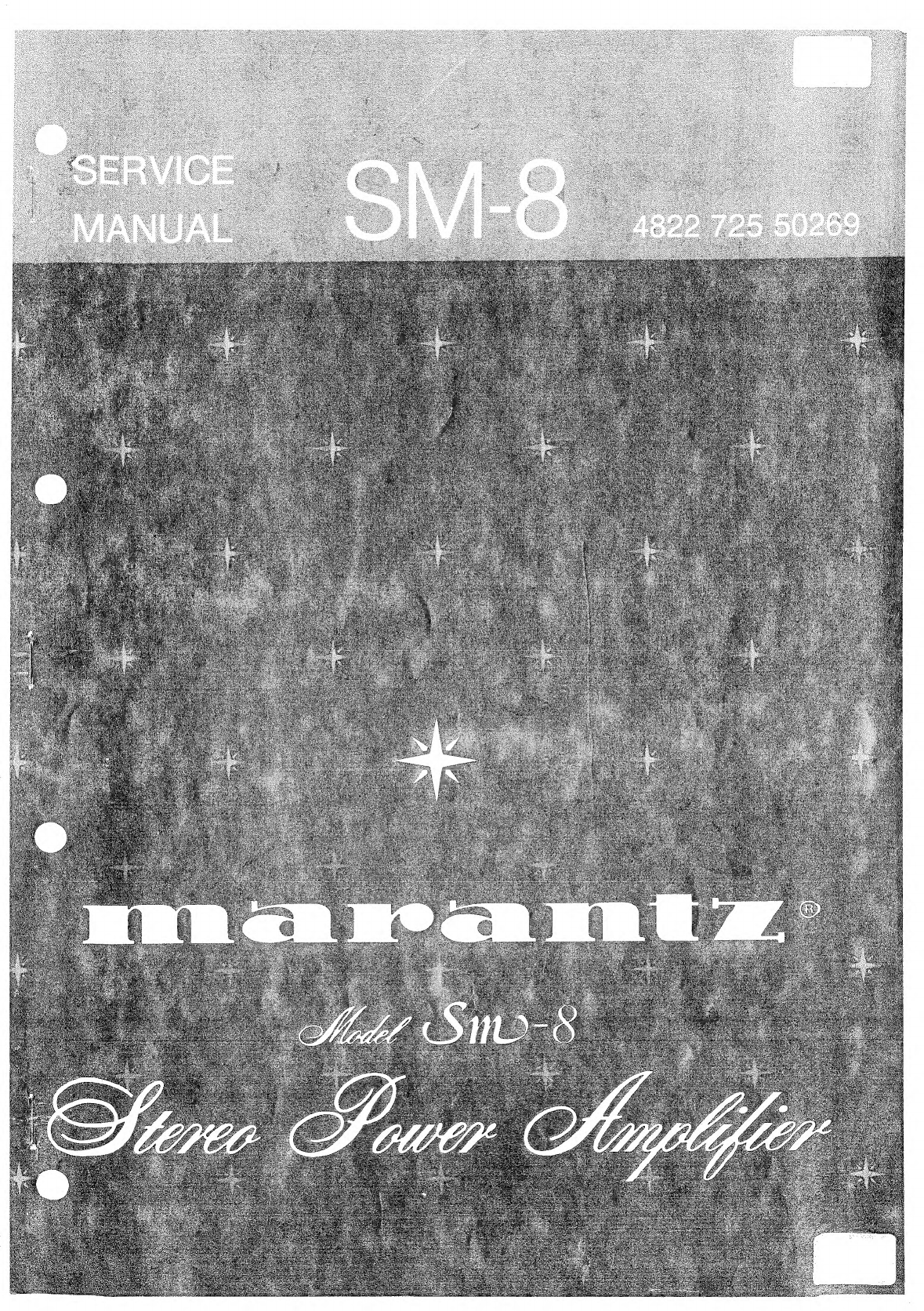
Marantz SM-8 User manual


MARANTZ
DESIGN
AND
SERVICE
Using
superior
design
and
selected
high
grade
components,
MARANTZ
company
has
created
the
ultimate
in
stereo
sound.
MARANTZ
INTERNATIONAL
Only
original
MARANTZ
parts
can
insure
that
your
MARANTZ
product
will
continue
to
perform
to
the
specifications
for
which
it
is
famous.
Parts
for
your
MARANTZ
equipment
are
generally
available
to
our
National
Marantz
Subsidiary
or
Agent.
ORDERING
PARTS:
Parts
can
be
ordered
either
by
mail
or
by
telex.
In
both
cases,
correct
part
number
has
to
be
specified.
The
following
information
must
be
supplied
to
eliminate
delays
in
processing
your
order:
.
Way
of
shipment
Onhwn
.
Complete
address
.
Complete
part
numbers
and
quantities
required
.
Description
of
parts
.
Model
number
for
which
part
is
required
Vestdijk
9
5600
MD_
Eindhoven
The
Netherlands
Phone:
+31/40.758290
.
Signature:
any
order
form
or
telex
must
be
signed
otherwise
such
part
order
will
be
considered
as
null
and
void.
PARTS
ORDERING
Parts
may
be
ordered
at
the
following
addresses:
AUSTRIA
MARANTZ
Hietzinger
Kai
137a
1130
Wien
BELGIUM
SVD
DIVISION
MARANTZ
Industrialaan
1
1720
Groot-Bijgaarden
Beigium
Telex:
24466
CHILE
MARANTZ
DIVISION
OF
PHILIPS
S.A.
AV.
Santa
Maria,
0760
Casilla
2687
Santiago
Telex:
240.239
DENMARK
MARANTZ
Horsvinget
5
2630
Tastrup
NORWAY
MARANTZ
Postboks
7034
Assiden
3007
Drammen
FRANCE
MARANTZ
FRANCE
4
Rue
Bernard
Palissy
92600
Asniéres
France
Telex:
611651
GERMANY
MARANTZ
GERMANY
GmbH
Alexanderstrasse
1
2000
Hamburg
Germany
THE
NETHERLANDS
Elpro
Marantz
Wint
Hontlaan
28
3526
KV
Utrecht
The
Netherlands
Telex:
4748
SWEDEN
MARANTZ
Box
1324
171
25
Solna
FINLAND
MARANTZ
Kuortanegatan
14
00520
Helsingfors
52
GREAT
BRITAIN
MARANTZ
HiFi
U.K.
Ltd
Kingsbridge
House
Padbury
oaks
575-583
Bath
Road
Long
ford
Middlesex
UB7
OEH
Faxnr.:
0753
680
428
GREECE
SHERTON
ELECTRONICS
S.A.
P.O,.Box
21025
Hippocratus
Street
188
Athens
11471
Greece
Telex:
216.795
JAPAN
MARANTZ
JAPAN,
Inc.
35-1,
7-chome,
Sagamiono
Sagamihara-shi,
Kanagawa
Japan
KUWAIT
AL
ALAMIAH
ELECTRONICS
Ussama
Building
Fahd
al
Saleem
Street
P.O.Box
23781
Safat-Kuwait
Telex:
22694
Telefax:
+31/40.75.82.99
Telex:
35000
PHTC
NL
routing
IND
NLMTFAT
ITALY
MARANTZ
ITALIANA
S.P.A.
Via
Chiese,
74
20126
Milano
Italy
SAUDI
ARABIA
AL
ALAMIAH
ELECTRONICS
P.O.Box
5954
University
Street
Riyadh
11432
Saudi
Arabia
Telex:
401530
SOUTH
AFRICA
MARANTZ
DIVISION
OF
PHILIPS
S.A.
Main
Road
Martindale
P.O.
Box.
58088
Newville
21114
South
Africa
SPAIN
Euroservice
S.A.
Bernardo
obrégon,
26
28012
Madrid
faxnr.:
3412
306
198
SWITZERLAND
MARANTZ
Technischer
Service
Duenstrasse
3
3186
Didingen
Switzerland
TURKEY
DOGRUOL
Ltd.
LM.C.
6
Blok
N°6310
Unkapani
Istanbul
Turkey
Telex:
22085
MALTA
CACHIA
&
GALEA
Republic
Street,
68D
Valetta
Telex:
1682
PORTUGAL
MARANTZ
Divisao
philips
S.A.
service
Outurela-carnaxide
2795
LinDA-A-VELHA
Telex:
43906
All
of
the
above
locations
are
fully
equipped
to
take
care
of
your
total
service
needs.
Because
various
countries
have
differing
configuration
requirements,
it
is
necessary
that
you
contact
the
service
facility
in
your
particular
country.
In
the
event
that
there
is
no
service
location
listed
for
your
country,
please,
contact
the
nearest
facility
for
the
necessary
In
case
of
difficulties,
do
not
hesitate
to
contact
the
Technical
Department
at
abovementioned
address.
assistance.

MARANTZ
MODEL
Sm-8
STEREO
POWER
AMPLIFIER
wenan
eran
cul.
INTRODUCTION
This
service
manual
was
prepared
for
use
by
Authorized
Warranty
Staions
and
contains
service
information
for
the
Marantz
Model
Sm-8
Stereo
Power
Amplifier.
Servicing
information
and
voltage
data
included
in
this
manual
are
intended
for
use
by
knowledgeable
and
ex-
perienced
personnel
only.
All
instructions
should
be
read
carefully.
No
attempt
should
be
made
to
proceed
without
a
good
understanding
of
circuitry
operation.
The
parts
list
furnishes
complete
ordering
information.
Most
replacement
parts
should
be
ordered
from
the
Marantz
Company.
However,
a
simple
description
is
included
for
parts
which
can
be
obtained
locally.
1.
SHOCK,
FIRE
HAZARD
SERVICE
TEST
CAUTION:
After
servicing
this
appliance
and
prior
to
returning
to
customer,
measure
the
resistance
between
either
primary
AC
cord
connector
pins
(with
unit
NOT
connected
to
AC
mains
and
its
Power
switch
ON),
and
the
face
or
front
Panel
of
product
and
controls
and
chassis
bottom.
Any
resistance
measurement
less
than
1
Megohms
should
cause
unit
to
be
repaired
or
corrected
before
AC
power
is
applied,
and
verfied
before
return
to
user/customer.
Ref.
UL
Standard
No.
1270.
Para.
66.
3.
D
(Mandatory
Test
after
servicing
Electrical
Appliances,
effective
7-1-83).
2.
FEATURES
@
High
power
—
120W
x
2
of
dynamic
“Marantz”
sound
From
the
line
input,
the
audio
signal
passes
to
the
dual
FETs
in
the
buffer
amp
and
then
to
the
first
stage
which
is
a
differential
amplifier
using
dual
transistors.
One
side
of
this
differential
output
is
phase
inverted,
while
the
output
of
the
buffer
amp
passes
to
a
pure
push-pull
amplifier
which
drives
the
final
output
stage.
The
power
amplifier
stage
uses
newly
developed
super
high
fT
power
transistors
in
parallel
three-stage
Darlington
connection.
This
makes
possible
handling
high
currents
with
sufficient
heat
radiating
capacity.

TABLE
OF
CONTENTS
SECTION
PAGE
INTRODUCTION)
2s
c55
2558
Se
Sak
Soe
ed
eee
ans
nals
SE
ices
eae
baa
oe
ee
SR
ee
ea
1
1.
SHOCK,
FIRE
HAZARD
SERVICE
TEST
..........
0...
0c cc
ccc
eee
eens
1
25
“FEATURES
(id
scnnitcaeeic
Be
eS
PR
eR
ee
a
Sieg
Be
ee
Bade
eS
hae
eee
Sd
1
3.
(PW:
BOARDS
iio
a5
Gees
ars
cette
ane
Boab
ol
wok
Dae
OG
Be
2
aah
ee
ae
be
ee
2
4.
TEST
EQUIPMENT
REQUIRED
FOR
SERVICING
....................
ccc
cee
cece
3
5.
ADJUSTMENT
PROCEDURES
.............
0.
ccc
cece
ec
eee
eee
eee
teen
eens
3
6.
VOLTAGE
-GONVERSION)
«3
c4-c:2-fh
dhcceb
ld
Ses,
Sb
oa
Serene
cans
Ble
ve
avg
Wed
See
ys
Wlaede
a
dee
ears
OS
4
7:
BEOCK
DIAGRAM
08
58
605
Nees
Sree
RE
re
Ree
be
a
ae
Ss
Re
5
8.
DIAGRAM
AND
COMPONENT
LOCATIONS
.............0..
0c
cece
cece
cence
ee ee
eens
6
8.1.
Voltage
Amp.
Assembly
(P700)
Schematic
Diagram
and
Component
Locations
...........
6000
ee
eee
6
8.2
Speaker
&
Meter
Switch
Assembly
(PSOO)
Schematic
Diagram
and
Component
Locations
.............+5
6
8.3
ASO
Protector-Assembly
(PNOO)
Schematic
Diagram
and
Component
Locations
............05
000008
7
8.4
A-B
Power
Switch
Assembly
(PKOO)
Schematic
Diagram
and
Component
Locations
..............+-+--
7
8.5
Power
Amp.
Assembly
(P600)
Schematic
Diagram
and
Component
Locations
.............0000ee0ee
8
8.6
Output
Network
Assembly
(PWOO)
Schematic
Diagram
and
Component
Locations
..............20005
8
8.7.
Test
Point
Assembly
(PJOO)
Schematic
Diagram
and
Component
Locations
..........0.0.
0000
ee
eee
8
8.8
Meter
&
Supply
Assembly
(PX00)
Schematic
Diagram
and
Component
Locations.............2.0080%
9
8.9
A-B
Detector
Assembly
(PLOO)
Schematic
Diagram
and
Component
Locations
.............00-2e00%
10
8.10
Connection
Assembly
(PP00)
Schematic
Diagram
and
Component
Locations
.............
000028088
10
9.
EXPLODED
VIEW
AND
PARTS
LIST
.....
0.0...
0.
ccc
ec
ce
eee
tenes
11
10.
(ELECTRICAL
PARTS
“UIST
>
vac
cee
iic5
concd:
oer
ae
arene
Sie
ESS
wie,
SME
ES
WE
WE
ta
Le
ads
as
18
11.
TECHNICAL
SPECIFICATIONS
.......
2.0...
0...
cc
ccc
ee
eee
eee
een
ne
aee
23
12.
SCHEMATIC
DIAGRAM
............
ccc
ccc
cect
eee
eee
tenn
e
tenet
seen
ee
eenes
24
Masts

@
Class
A
—
Class
AB
automatic
switching
circuit
3.
P.W
BOARDS
Quarter
A
allows
the
main
amplifier
to
operate
as
a
pure
class
A
amplifier
for
outputs
of
up
to
30W,
which
is
a
quarter
of
the
rated
output
120W
at
8Q,
at
the
switch
to
class
AB
for
outputs
larger
than
30W.
The
transition
from
class
A
to
class
AB
or
vice
versa
is
carried
out
by
switching
the
bias
current
and
the
power
supply
voltage.
As
can
be
seen
from
the
circuit
diagram
the
chassis
of
Mode
Sm-8
consists
of
the
following
units.
Each
unit
mounted
or
a
printed
circuit
board
is
descrided
within
the
square
enclosed
by
a
bold
dotted
line
on
the
circuit
diagram.
The
automatic
switching
circuit
monitors
the
input
volt-
1.
PowerAmp.
.......
mounted
on
P.W.
Board
P60C
age
of
the
main
amplifier
and
the
output
current
of
the
2.
Voltage
Amp.
.....-
mounted
on
P.W.
Board
P70C
speaker
in
order
to
detect
output
transitions.
Note
that
3.
Test
Point.........
mounted
on
P.W.
Board
PJOC
the
use
of
a
phase
correction
circuit
inside
the
detector
4.
A-B
Power
Switch.
..
.
mounted
on
P.W.
Board
PKOC
prevents
waveforms
including
those
with
a
steep
rising
5.
A-B
Detector.......
mounted
on
P.W.
Board
PLOC
edge
from
being
distorted.
The
automatic
switching
6.
ASO
Protector
......
mounted
on
P.W.
Board
PNOC
circuit
can
be
easily
used
for
amplifier
configurations
7.
Connection
........
mounted
on
P.W.
Board
PPOC
uniquely
designed
by
Marantz
by
merely
connecting
the
8.
Speaker
&
input
of
the
detector
to
the
signal
system.
Meter
Switch
.......
mounted
on
P.W.
Board
PSOC
9.
Output
Network.....
mounted
on
P.W.
Board
PWOC
10.
Meter
&
Supply
.....
mounted
on
P.W.
Board
PXOC
@
Large-sized
peak
power
meter
of
the
logarithmic
com-
pressed
type
Large-sized
power
meters
that
are
suitable
for
high
quality
power
amplifiers
are
available.
This
power
meter
can
be
used
to
check
the
output
level
and
the
balance
between
the
right
and
left
channels.
It
operates
by
detecting
signal
peaks,
but
it
displays
rms
values
which
directly
represent
the
outputs
of
the
amplifier
to
an
8Q
load.
In
addition,
since
a
circuit
generating
logarithmic
com-
pressed
displayes
is
used,
outputs
of
small
to
large
quantities
can
be
monitored
without
changing
the
range.
This
power
meter
can
also
be
used
as a
peak
holder
by
setting
appropriate
switches
on
the
panel.
@
Protective
circuit
which
does
not
degrade
tone
quality
The
overload
protective
circuit
detects
both
overvoltage
and
overcurrent
conditions,
while
in
the
area
of
safe
operation
(A.S.O.)
does
not
degrade
the
operation
of
the
drive
transistors.
The
protective
circuit
has
adaptable
characteristics
so
that
its
operation
does
not
interfere
with
the
program
and
its
operation
is
always
constant.
e
Plus
The
power
output
circuit
is
equipped
with
high
efficiency
heat
sinks
to
cool
the
power
transistors,
thus
providing
continuous
high
output
power.

4.
TEST
EQUIPMENT
REQUIRED
FOR
SERVICING
This
table
lists
the
test
equipment
required
for
servicing
the
Model
Sm-8
Stereo
Power
Amplifier.
Distortion
Analyzer
Distortion
measurements
Audio
Oscillator
AC
VTVM
Oscilloscope
Sinewave
and
squarewave
signal
source
Voltage
measurements
(AC)
Waveform
analysis
and
trouble
shooting
and
ASO
alignment
|
Circuit
Tester
DC
VTVM
Trouble
shooting
Voltage
measurements
(DC)
AC
Wattmeter
Line
Voltmeter
Variable
Autotransformer
(0
~
140V
AC,
10A)
Monitors
primary
power
to
amplifier
Monitors
potential
of
primary
power
to
amplifier
Adjust
level
of
primery
power
to
amplifier
Shorting
Plug
5.
ADJUSTMENT
PROCEDURES
1.
Class
B
idting
adjustment
a)
Apply
a
sine
wave
signal
of
1
to
2
VRMS
to
JL14
from
an
audio
oscillator
in
order
to
forcibly
make
it
Operate
as
a
class
B
amplifier.
b)
Adjust
RL43
and
RL44
so
as
to
give
DC
voltage
of
7
mV
at
the
JJO1-02
and
JJ03-04
test
points.
NOTE:
Carry
out
the
adjustment
one
minute
after
the
switch
is
turned
on.
After
the
set
is
stabilized,
the
voltage
should
be
27
mV
(50
mA).
2.
Class
A
idling
adjustment
a)
Disconnect
the
input
to
JL14.
b)
Adjust
RL39
and
RL40
so
as
to
give
DC
voltage
of
440
mV
at
the
JJO1-02
and
JJ03-04
test
points.
NOTE:
Carry
out
the
adjustment
one
minute
after
the
input
to
JL14
is
disconnected.
The
class
B
ad-
justment
must
be
done
first.
After
the
unit
is
stabilized,
the
voltage
should
be
370
mV
(655
mA).
3.
Comparator
balance
adjustment
a)
Connect
a
trigger
oscilloscope
to
JL14.
b)
Set
the
load
of
the
device
to
OPEN,
apply
a
signal
with
a
frequency
of
1
kHz
and
increase
it
gradually.
c)
While
observing
the
output
waveform
of
the
unit
and
pulses
at
JL14,
adjust
RL31
so
as
to
generate
two
pulses
per
output
waveform
period.
Shorts
amplifier
input
to
eliminate
noise
pickup
rae
acs
Output
waveform
+5V
|
|
JL14
T.P
Ov
4.
Switching
level
adjustment
a)
Connect
a
trigger
oscilloscope
to
JL14.
b)
Set
the
load
of
the
unit
to
OPEN
and
apply
a
signal
having
a
frequency
of
1
kHz
to
the
L
channel.
c)
With
the
output
set
to
15.5V,
adjust
RLOQ
so
as
to
generate
pulses
at
JL14.
d)
Apply
a
signal
to
the
R
channel
and,
similarly,
adjust
RL10.
5.
Power
meter
adjustment
a)
Set
the
load
of
the
unit
to
8Q,
apply
a
signal
having
a
frequency
of
1
kHz
and
increase
the
input
signal
to
30.9V.
b)
Adjust
the
following
so
as
to
give
a
reading
of
120V
on
the
meter.
For
the
L
channel,
adjust
R
X05.
For
the
R
channel,
adjust
RX06.

6.
VOLTAGE
CONVERSION
7.
BLOCK
DIAGRAM
@
EUROPEAN
MODEL
ONLY
OUTLET
BEFORE
CONVERTING
VOLTAGE.
™N
nd
OOOO
S
>
To
convert
the
unit
to
a
different
power
source
voltage,
oS
oe
oe
a
is
change
the
position
as
illustrated
in
the
drawing
below.
7
CAUTION
=5
fy.
3
¥e
=
DISCONNECT
POWER
SUPPLY
CORD
FROM
AC
==
5
a=
OOOO
=
>
n
2
oO
—
oO
Lhd
=
oOo
co
a.
oc
SZ
>
Sos
oO
cw
nac
Voltage
Conversion
Chart
o
=
==
oO
ES
Be
[Sei
Ocry
xoa
sSusa
we
Secs
o
=S>an
Oo
_
r=}
o
=
s
1
a.
'
I
Bea
l
t
!
!
!
|
2
|
YW
io=
I
S26r
*
1s
pa
bbl
—
efbs
=o
oF
aoe
n=
SaaaG
s=
oD
12
ox
wc
==
t=
aa
2a
\
e
1s
n
Mo
i]
—
=
4
[aad
(<<
2s
=
1s
a?
oc
oc <z
1c
uy
WH
kd
[oad
=>
oe
>=
=>
=<
<<
VOLTAGE
uo
ES
ea
1
a
we
-—2
<=
D
SELECTOR
oo
oa
3
1
<
oo
2a
=
'
{
t
!
t
x
|
oad
=z
Lon
'
=
=
'
=
©
{
[we
co
{
wey
a
!
—
oa
|
_——_—
Note
on
safety:
Symbol!
A\
Fire
or
electrical
shock
hazard.
Only
orignal
parts
should
be
used
to
replace
any
part
marked
with
symbol
A
.
Any
other
component
substitution
(other
than
original
type),
may
increase
risk
of
fire
or
electrical
shock
hazard.

8.
DIAGRAM
AND
COMPONENT
LOCATIONS
330
0729
R739
2s
(-1.69V)
(-2.08V)
7h
€65.6V)
R749
12k
8.1
Voltage
Amp.
Assembly
(P700)
Schematic
Diagram
and
Component
Locations
8.3
ASO
Protector
Assembly
(PNO0)
BrOG
VOLTAGE
ANE
LASSY.
a
Schematic
Diagram
and
Component
Locations
me
moe’
R74)
R782
4a.7k
4.7K
330
47k
|
(63.4V)
R785
33k
|
(630v)
Or"
own
cr
109780
0]
|
|
C67)
(2.08V)
20
P
t
Q709
S
Q713
‘E
|
3
4
le
75
ike
|
oy
am
eatin
hes
K
a7i9
C74.0V)
(620V)
CK)
R248
|
5
—O
om
O
©
ae)
©
©
O
~O
O
|
[oy
R738S
R742
(eD.BY,
|
|
4.7K
S
330
(F)
ONLY
220/100V
0718
_|
[e775
+,,100/80Vv
G3.5v)
cex00l
(¥
C777_0.001
aval
K)
R779,\.
47k
ve
167)
(2.08V)
O77)
A
KC)
aria
=p
Q710
OH
:
777
KH
:
PS
ee
x
D>
a8
‘NO
8
C4077
ey
ee
&
Or73
‘aidan
(ov)
9779
7)
c779
1000p
Q716
61.69V)
R732
A
m3
ed
J
708
UN
0720
Rr
eu)
R735
C143)
4.7K
(63.0V),
K)
R744
740
Ul
i
663.3)
656)
C7I2
0.47/00V
R
|
Q722
2/2
PSOO

8.5
Power
Amp.
Assembly
(P600)
Schematic
Diagram
and
Component
Locations
8.6
Output
Network
ilariall
wisbbeas
Schematic
Diagram
and
pompuren
Locations
|
P60O0
POWER
AMP
and
PROTECTOR
|
|
R6EIZ
47
wy
Kk
saa
iy
R607
|
REO!
Q603
C60!
27k
270p
623
0.047
rR
O
Oo
A
..
é
5
On
So
os
=
O
rae
O
O
3
5
Oo
a
5
O
A
5
O
2°
|
rf
JOS
9)
(Sw)
R626
R644
wze|
f°
cer
sas
(WQ61
9636
|
ee
(43.50)
R646
We
K)
raw
Visine
47k
er,
5s?
Q6i8
L___
3
or
A
We
y
a
a
nett
3
S080)
(-L46V)
2
|
jeosow
an
:
CE05UN-270V)
(-0.79V)
Q620
TT
\
oe
Bore
art
oe
2
iw
oe
R
"Sens
anmeestectonseonr
cc
ene
sreamestrit
onetime
aeenteaner
enn
22.0)
Q640
Q624
&
&
%&
ret
6
ov
tes”
os
8.8
Meter
&
Supply
Assembly
re:
Schematic
ee
and
Component
Locations
220780v
|
[COV
5s
leech
€74.0V)
2
[|
|
Olvliolz
ee
HO
00
OO
eee
OD
L
[
BS
of
O~
t
=
x
5
rr)
Yo
x
5S
8.7
Test
Point
Assembly
(PJ00)
Schematic
Diagram
and
Component
Locations
JJO1
JJO2

9.
EXPLODED
VIEW
AND
PARTS
LIST
8.9
A-B
Detector
Assembly
(PLO0)
Schematic
Diagram
and
Component
Locations
@
[C01-99]
Front
Panel
0058
7)
-“@
Be
Ge
QLO3-1/4
021B
,
@(U):
for
U.S.A
e
(E):
for
Europe
e(F):
for
Japan
PART
NO.
DESCRIPTION
222H063400
Front
Panel
Assembly
222H063010
Escutcheon,
Front
Panel
2461063030
Escutcheon,
Pocket
Frame
2144160020
Bracket
222H063020
Escutcheon,
Pocket
Panel
51060305A9
|
P.H.M.
Screw
P3
x5
2461271010
Holder
51042610A0
F.H.M.
Screw
F2.6
x
10
53112603A0
|
Hexagon
Nut
M2.6
51100204E0
B.H.M.
Screw
B2x4
1143259010
Bushing,
Pin
Holder
2978259110
Bushing,
Push
Switch
201H158010
|
Window,
Meter
2461063420
Pocket
Cover
Assembly
2144063410
Pocket
Cover
Assembly
2461063050
Escutcheon,
Pocket
Cover
2461253010
Handle
2461253210
Handle
2461254010
Pin
2461254020
Pin
53110303E9
Hexagon
Nut
2461107020
Sheet
][]
P
ABH
NNN
|
oa
oo
oa
a
[|=
RPRANNNA
DY
BW
ean
a
—"-
PEPNNNAHND
awa
wa
51500308Z0
F.H.
Tapped
Screw
F3
x
6
51280308Z0
B.H.
Tapped
Screw
B3
x
8
10

@
[C02-99]
Top
Cover
(F)
TYPE
¢(U):
for
U.S.A.
+(E):
for
Europe
¢(F):
for
Japan
Q'ty
PART
NO.
DESCRIP
TION
Lid,
Top
Cover
Case
Wood
Spacer
Punched
Plate
Bushing
Punched
Plate
B.T.
Screw
B3
x8
B.H.
Tapped
Screw
B4
x
30
Labe
2911861140
2911861110
2461257010
222H064500
2965118010
2996003010
2991259110
222H003010
5126030820
51280430U0
222H861020
5148040629
F4x6
54080400R0
59030805S0
53250503A0
222H861010
2144257010
2759057010
51280410U0
51280406U0
2759057010
51570410U0
51524116A0
F.Washer
Screw
T.L
Washer
Washer
Special
Nut
Label
Lid,
Bottom
Cover
Leg
B.H.
Tapped
Screw
B4
x
10
B.H.
Tapped
Screw
B4
x6
Leg
P.
Taptite
Screw
P4x
10
R.H.
Wood
Screw
12

@
[C03-99]
Rear
Panel
@(U):
for
U.S.A.
@(E):
for
Europe
@(F):
for
Japan
N=
P=NNN=O
“hon
PART
NO.
DESCRIPTION
vie
Oe
eee
222H160230
Bracket,
Rear
Panel
222H160220
|
Bracket,
Rear
Panel
222H160210
|
Bracket,
Rear
Panel
51100308Z9
|
B.H.M.
Screw
B3
x8
51260308ZO
|
B.T.
Screw
B3
x8
1455259090
Bushing,
AC
Power
Cord
1455259050
Bushing,
AC
Power
Cord
1455259120
Bushing
51260308Z0
|;
B.T.
Screw
B3
x8
62040029W0
|
Lug,
GND
54040502A0
|
Spring
Washer
201H053030
Cover,
Voltage
Selector
51280308U0
|
B.H.
Tapped
Screw
B3
x
8
51280308U0
|
B.H.
Tapped
Screw
B3
x
8
51260308Z0
B.T.
Screw
B3
x8
221H267010
|
Heatsink
51780312Z0
B.T.
Screw,
Fin
Neck
B3
x
12
5402030120
Flat
Washsr,
P
2112265010
4581861010
Indicator,
Serial
No.
Label
Bracket
B.T.
Screw
B.T.
Screw
404H160030
51260308Z0
51260306Z0
B3x8
B3
x6
+10%
+10%
+10%
+£10%
%”W
DF76104120
DF76332570
DF76332570
RC10104120
Film
Cap.
0.1pF
Film
Cap.
3300pF
Film
Cap.
3300pF
Resistor
100K2
DESCRIPTION
PART
NO.
FS10800020
FS10400900
FS10800600
YJ08000310
YJ08000290
YJ08000300
YJ04000910
YJ04000910
BY05080010
YT01010050
YT02020170
Y¥T01010100
YT01010710
YT01010100
Y¥T01010110
Y¥T01010100
YT01010110
YT01010100
YT01010110
1
1
1
1
1
1
1
1
-
oe
ek
ot
oe
os
YC02000160
YC01900090
YC01800240
13
8A
4A
8A
250V
250V
250V
Fuse
Fuse
Fuse
Jack,
Fuse
Holder
Jack,
Fuse
Holder
Jack,
Fuse
Holder
Jack,
AC
Outlet
Jack,
AC
Outlet
Voltage
Selector
Terminal,
GND
Terminal,
(2P)
RCA
Pin
Jack
Terminal,
SPK
System
1;
Red
Terminal,
SPK
System
1;
Black
Terminal,
SPK
System
1;
Red
Terminal,
SPK
System
1;
Black
Terminal,
SPK
System
2;
Red
Terminal,
SPK
System
2;
Black
Terminal,
SPK
System
2;
Red
Terminal,
SPK
System
2;
Black
A.C.
Power
Cord
A.C.
Power
Cord
A.C.
Power
Cord

e@
[P01-99]
Front
Chassis
and
General
Parts
PART
NO.
|
DESCRIPTION
2970154630
Knob,
Push
Switch
201H160010
201H160110
51100306A9
5110030829
201H118010
222H063030
201H053120
51260308Z0
201H053010
201H274010
Bracket,
Front
Chassis
Bracket,
Front
Chassis
B.H.M.
Screw
B3
x6
B.H.M.
Screw
B3
x
8
Spacer
Escutcheon,
Meter
Cover
B.T.
Screw
Cover,
Meter
Reflector,
Meter
NNNNANN
A
NNNNANN
AS
NNNNANNA
=
201
H274020
5126030820
51280312Z0
5126030620
201H303010
205H160110
51400335P0
205H120010
Reflector,
Meter
B.T.
Screw
B3
x8
B.H.
Tapped
Screw
B3
x
12
B.T.
Screw
B3
x6
Mask,
Meter
Bracket
B.H.
Tapped
Screw
B3
x
35
Insulator
NNPAPN
NNA
AN
Pe
PNNAHPN
vlelF|
ee
oe
bd
ot ob
ot
od
O19G
q
PART
NO.
1M11098020
1IM11098020
1N10080540
1N10080540
BF10400030
DK18103840
DF
16104510
SP01010550
SP01010560
SP01010540
5128031220
DF17104520
DF17104520
DF17104520
DF17104520
EC68710010
EC68710010
HD20004290
HD20022290
.
DESCRIPTION
S&S
0266
a
ae
028G
0(U):
for
U.S.A.
»°(£):
for
Europe
0(F):
for
Japan
D.C.
Meter
D.C.
Meter
Lamp,
8V
300nA
Lamp,
8V
300nA
Cap.
Comp.
0.3
uF
+1202
Ceramic
0.4
uF
Film
Cap.
0.BuF
+10%
Push
Switch,
Pewer
Push
Switch,
Power
Push
Switch,
Pewer
B.H.
Tapped
Scew
B3
x
12
Film
Cap.
0.4
+20%
200V
Film
Cap.
0.4
+20%
200V
Film
Cap.
O.uF
+20% 200V
Film
Cap.
0.4
+20%
200V
Elect
Cap.
680,
100V
Elect
Cap.
680:
100V
Diode
$5\B
-20
Diode
S4\B
-20

e@
[P02-99]
Main
Amp.
P.W.
Board
and
Heatsink
042L
OOSR
028E
dd
Ys
Ee
t06r
OO5F
SS
.
15

e@(U):
for
U.S.A.
@(E):
for
Europe
e
(F):
for
Japan
PART
NO.
DESCRIPTION
[ue]
F|
2144105010
|
Chassis,
Center
O53L
{1/1/11}
2144123040
|
Contactor
2144105110
|
Chassis,
Center
054L
|1|111/
2144123050
|
Contactor
2979105220
|
Chassis,
Side
(R)
O55L
|1/1/1{|
2144123060
|
Contactor
11
2979105120
|
Chassis,
Side
(R)
o60L
|1/1/]1/|
222H267030
|
Heatsink
(1)
1
2979105230
|
Chassis,
Side
(L)
061L
|2|
2]
2]
51100308Z9
|
B.H.M.
Screw
B3
x8
1|
2979105130
|
Chassis,
Side
(L)
062L
|1|1|1)
222H267040
|
Heatsink
(2)
6|6|
5126040820
|
B.T.
Screw
B4x8
063L
|3/3)3/
51280312Z0
|
B.H.
Tapped
Screw
B3
x
12
41
4|
51260308Z0
|
B.T.
Screw
B3
x8
064L
1414/4!
51280312Z0
|
B.H.
Tapped
Screw
B3
x
12
4|
4|
5148040629
F.
Washer
Screw
F4ax6
O65L
4|
222H053010
|
Cover
4}
4]
5126030820
B.T.
Screw
B3
x8
1|1)1]
221H123010
|
Contactor
027E
11
62030039WO
|
Lug
1|1]
1]
221H160010
|
Bracket
028E
1|
51280308Z0
|
B.H.
Tapped
Screw
B3
x
8
021F
|1/1|
1)
221HO67010
|
Cap
O44F
|1/14|1{
51260308Z0
|
B.T.
Screw
B3x8
O45F
|2|2|
2]
51260308Z0
|
B.T.
Screw
B3
x8
005R
1
2882861020
Label
O5SO0F
|1/1
2144160090
|
Bracket
O50F
1|
2144160190
|
Bracket
O51F
|2)2]|
2]
51500308Z0
|
F.H.
Tapped
Screw
F3x8
coo1
|1/1/1)
€C22907520
|
Elect
Cap.
22000uF
75V
052F
|2|2j)
2|
51280306Z0
|
B.H.
Tapped
Screw
B3
x6
cooz
|1/1/1]
EC22907520
|
Elect
Cap.
22000uF
75V
O54F
|1/1)
1)
62030049W0
|
Lug
coo3
|1/1/|1)/
EC20903510
|
Elect
Cap.
20000uF
35V
2]
222HO53020
|
Cover
cooa
|1/11/1|
EC20903510
|
Elect
Cap.
20000uF
35V
62030039WO
|
Lug
51280308B0
|
B.H.
Tapped
Screw
ALOO1
|1
TS60508080
|
Power
Transformer
ALOO1
1
TS60508070
Power
Transformer
ALOO1
1
|
TS60508060
Power
Transformer
oot
|1 1] 1]
222H267020
|
Heatsink
o02L
[1]
1
2144160040
|
Bracket
ROO1
|1
1/1]
GS10222030
|
Resistor
2.2K9
+10%
3W
002L
1]
2144160140
|
Bracket
R002
|1/1]|1|
GS10222030
|
Resistor
2.2K9
+10%
3W
oo3L
|
141
2144160050
|
Bracket
AROO3
|1/1|1
|
GJ05332020
|
Resistor
3.3K0
+10%
2W
003L
1|
2144160150
|
Bracket
AROO4
|1
1/111]
GJ05132020
|
Resistor
1.3K9
+£10%
2W
004L
+
|4/]
4]
4]
51260306Z0
|
8.T.
Screw
B3
x6
OO6L
|2/2|
2]
201H120010
|
Insulator
woo2
|1/
11]
YU08200260
|
Jumper
Lead,
(8?)
200mm
008L_
|8/|8}|
8]
5273031029
|
H.S.
Heat
Bolt
H3
x
10
woo3
|1/1
1]
YU06200260
|
Jumper
Lead,
(6?)
200mm
009.
|8/8]
8]
54020301E0
|
Flat
Washer,
P.
010L.
18/8]
8|
54040302NO
|
Spring
Washer
Q601
|1/1/1]|HT315681S0
|
Transistor
2SCi681(S)
a6o2
|1/1/1|HT315681S0
|
Transistor
2SCi681(S)
oul
|1/1
222H160030
|
Bracket
0771
|1/1|1/|HT322382E0
|
Transistor
2SC2238(O
or
Y)
O11L
1|
222H160130
|
Bracket
Q772
11/111]
HT109682E0
|
Transistor
2SC68(O
or
Y)
012L
|2|2/
2}
51260308Z0
|
B.T.
Screw
B3x8
013L_
[2/2]
2}
51260308Z0
|
8.T.
Screw
B3
x8
O16L
|
1114]
1}
2886005020
Clamper
019L
|
2]|2]|
2|
2990267080
|
Heatsink
020L
|
2|2]|
2|
201H115010
|
Spring
022L
|4|4]|
4}
2212267020
|
Heatsink
023L
|4/|4|
4]
51260308Z0
|
B.T.
Screw
B3x8
024L
«=|
4/4)
4)
5128030820
B.H.
Tapped
Screw
B3
x
8
032L
|2|2|
2|
51260308Z0
|
B.T.
Screw
B3x8
033L
«}1/1/]
1)
2887005110
Clamper
034L
+|1/1/1/
51280308Z0
|
B.H.
Tapped
Screw
B3
x
8
O40L
|1/|1/|1]
2144160160
|
Bracket
041L
|3|3|
3]
51260308Z0
|
B.T.
Screw
B3x8
042L
+|2/|2/
2]
51260308Z0
|
B.T.
Screw
B3x8
047L
~+|2)
2]
2|
51260306Z0
|
B.T.
Screw
B3x6
o4sL
|4|4]|
4|
51260306Z0
|
B.TappedScrew
B3x6
o50L
|
4}|4|
4}
S59030808PO
|
Washer
051L
|
2|2|
2|
2144118010
|
Spacer
16

@
[H01-99]
Packing
Materials
222H801020
222H801010
222H801030
9090808030
9091111030
2144809020
204H053010
2864804010
2864804010
2139809010
205H809010
2139809020
9526019010
9526019060
9526019040
2144807010
205H807010
2731821010
Packing
Case
Packing
Case
Packing
Case
Polyethylene
Sheet
Polyethylene
Sheet
Cushion
Cover
Sleeve
Sheet
Cushion,
(R)
Cushion
Cushion,
(L)
Serial
No.
Card
Serial
No.
Card
Serial
No.
Card
Reinforcing
Reinforcing
Silicagel
009S
007T
SC
\
003S
004S
020S
ol2s
ools
(U,E)
TYPE
@
(U):
for
U.S.A.
@
(E):
for
Europe
@
(F):
for
Japan
PART
NO.
DESCRIPTION
ULE]
F
222H851010
|
Instructions
222H851310
|
Instructions
222H851110
|
[Instructions
222H851020
|
Instruction,
Spec
222H851320
|
Instruction,
Spec
9631000130
Guarantee
Card
103H854010
|
Guarantee
Card
222H856010
|
Circuit
Diagram
2225813010
Envelope
128T854010
Guarantee
Card
9560000100
Hang
Tag
9611000030
|
User's
Card
17

10.
ELECTRICAL
PARTS
LIST
PART
NO.
DESCRIPTION
YK222H1310
Z22222H8310
Peoo
j1/1/1
c6o1
|1/1)
1)
DF55271510
C602
|
1/41)
1)
DF55271510
cé6o3
|111/]1/
EA10703560
C604
|1
41]
1}
EA10703560
C605
{1
/1}|
1}
OF16104350
c606
=j|1/1/)
1)
DF16104350
C613.
|
141)
1}
EA10505030
c6i4.
|1/1/|
1}
EA47602530
C615
|111)
1}
EA22601630
cé16
«|
1/1
EA22710030
C617
«|
1/1
EA22710030
C623.
{1
/1)
1)
OF
16473350
C624
+
|1{1)
1)
DF16473350
C626
«|
1
1)1/|
1)
EA10602530
c629
|
1/1]
1|
DF16473350
c630
|
1/1)
1)
DF16473350
C632.
«|
1:
|
1]
1)
DF16222350
C633.
«|
1:|
1] 1)
DF16105540
c634.
41]
1/1)
DF16105540
R601
|1
|1]
1|
GDO5472140
R602
|1 1)
1)
GD05472140
R603
|
1/1)
1|
GD05153140
R604
|1
11)
1}
GD05153140
R605
|1 1) 1)
GD05103140
R606
{1
|1/
1|
GDO5103140
R607
|1
|1|
1}
GD05273140
R608
|1
11}
1}
GD05273140
R609
|1
11]
1)
GDO05273140
R610
1
|1|1]
1|
GD05273140
R611
|1
11]
1)
GDOS821140
R612
|1
11]
1|
GDOS821140
R613
|
141}
1)
GGO5470140
R614
|1
|1]
1)
GGO5470140
R615
{111}
1}
GGO5470140
R616
|1
11)
1)
GGO5470140
R617.
|
111]
1|
GGO5471140
R618
|
1)1|
1)
GGO5471140
R619
{1
|1}
1)
GA05562010
R620
|1/1]
1|
GAO5562010
R621
1111]
1|
GGO5330140
R622
1111/1]
GGO5330140
R623.
|
111]
1|
GGO5330140
R624
|1
1/1)
GGOS330140
R625
|
111}
1)
GGO5470140
R626
|1
11]
1}
GGO5470140
R627
|
1/1]
1}
75061001P0
R628
|1|1
|
1|
75061001P0
R629
[1
|1|
1!
GGO6220140
R630
|1
11]
1|
GGO5220140
P600-POWER
AMP.
CIRCUIT
BOARD
P.W.
Board,
Power
Amp.
P.W.
Board
Assembly
PG600-CAPACITORS
Film
270pF
+5%
Film
270pF
+5%
Elect
100uF
35V
Elect
100uF
35V
Film
O.1uF
+10%
Film
O.1uF
+10%
Elect
wr
50V
Elect
47uF
25V
Elect
22uF
16V
Elect
220uF
10V
Elect
220uF
10V
Film
0.047uF
+10%
Film
0.047uF
+10%
Elect
-
10uF
25V
Film
0.047uF
+10%
Film
0.047uF
+10%
Film
2200pF
+10%
Film
tuF
+10%
Film
ipF
+10%
P600-RESISTORS
(All
Resistors
are
+5%
and
%W)
4.7KQ
4.7K2
15K2
15K2
10KQ
10K
27K
27K2
27KQ
27KQ
8202
8202
472.
472.
472
472
4702
4702
5.6KQ
5.6KQ
332
332
332
332
472
472
Jumper
Jumper
222
222
18
Q’TY
e
(U):
for
U.S.A.
e
(E):
for
Europe
e
(F):
for
Japan
REF.
DESIG.
ul
EIE
PART
NO.
DESCRIPTION
——
R631
1111/1}
GG05220140
222
R632
|1/1/
1)
GGO5220140
222,
R633
|1}1
|
1)
GG05220140
222.
R634
|1}1]
1)
GGO05220140
222
R635.
|
1/1]
1)
GG05220140
222
R636
{1/1
|
1|
GGO5220140
222
R637.
|1/11
|
1)
GO10272050
0.272
+10%°
SW
R638
|}1/1
|
1}
GO10272050
0.272
+10%
5W
R639
11/111}
GO10272050
0.272
+10%
5W
R640
|1
1141)
GO19272050
0.272
+10%
5W
R641
111]
1]
GO10272050
0.272
+10%
5W
R642
|1/1
|
1}
GO10272050
0.272
+10%
5W
R643
{1
|
111)
GO10272050
0.272
+10%
5W
R644
{1/141
)
GO10272050
0.272
+10%
SW
R645
[1/1]
1)
GD05472140
4.7KQ
R646
|1/}1
|
1|
GD05472140
4.7KQ
R649
1111/1)
GDO5682140
6.8KQ
R650
|1/1/|
1)
GD05102140
1K
R651
1
|1|1}
GD05273140
27K2
R652
|1/1
|
171)
GD05273140
27KQ
R657.
|1
|
111)
GDO5823140
82K
R658
{1/1
|1/|
GD05823140
82K
R659
+|1/1
|
1)
GD05154140
150KQ
R660
|1/1
|
1)
GDO5183140
18K
R661
|1
11}
1)
GD05473140
47KQ
R662
|1/1/
1)
GD05473140
47K
R663
|1/1|
1)
GD05474140
470KQ
R664
{1/1}
1)
GD05273140
27KQ
R666
{1/1
|
1|
GDO5223140
22K2
R667
_|1|1
|
1}
GGO5183120
18K2
~W
R671
[1
}1
|
1|
GAO05562010
5.6K2
iW
R672
|1|1]
1}
GA05562010
5.6K
IW
R673
|1
|
1}
1}
GJO5100010
102
Iw
R679
|141/1}
GD05471140
4702
R680
j1/)1)1]
GD05471140
4709
P600-SEMICONDUCTORS
a6o1
|141/1]|HT315681S0
|
Transistor
28(1568(S)
a602
|1/111|H1T315681S0
|
Transistor
2S¢1568(S)
Q603
|1/}11|1)HT110152A0]
Transistor
2S41015(0
or
Y)
a604
111/141]
HT110152A0]
Transistor
2SA1
O15(0
or
Y)
a605
|1
1/1/11}
HT326322R0|
Transistor
2$(2632(R
or
S)
a606
|1/1/}1)HT326322RO0;
Transistor
2S(2632(R
or
§)
0607
|111|1|HT111242R0|
Transistor
25414
24(R
or
S)
asos
[1
/11/1]HT111242RO|
Transistor
2S\19
24{(R
or
S)
a6o9
|1/1/1]HT325912B0
|
Transistor
2S¢2&91(Q
or
R)
0610
{1/1/14
|H1T111112B0
|
Transistor
2541411
(Q
or
R)

e@(U):
for
U.S.A.
e(E):
for
Europe
@(F):
for
Japan
ee
[rn
EA47701630
|
Elect
470nF
EA47701630
|
Elect
470uF
EA47601630
|
Elect
47uF
EA10710030
|
Elect
100u
F
EA22710060
|
Elect
220uF
EA10710030
|
Elect
100u
F
EA22710060
|
Elect
220uF
DF16102510
|
Film
1000pF
+10%
DF16102510
|
Film
1000pF
+10%
DF16102510
|
Film
1000pF
+10%
DF16102510
|
Film
1000pF
+10%
Q’TY
oss,
ater
PART
NO.
DESCRIPTION
HT325912B0
|
Transistor
2SC2591(Q
or
R)
HT111112B0
|
Transistor
2SA7111(Q
or
R)
HT328372A0
|
Transistor
2SC2837(R
or
O)
HT111862A0
|
Transistor
2SA1186(R
or
O)
HT328372A0
|
Transistor
2SC2837(R
or
O)
HT111862A0
|
Transistor
2SA1186(R
or
O)
HT328372A0
|
Transistor
2SC2837(R
or
O)
HT111862A0
|
Transistor
2SA1186(R
or
O)
HT328372A0
|
Transistor
2SC2837(R
or
O)
HT111862A0
|
Transistor
2SA1186(R
or
O)
ee
ee
es
HT318152A0
|
Transistor
25C1815(O
or
Y)
HT318152A0]|
Transistor
2SC1815(O
or
Y)
HT110152A0]|
Transistor
2SA1015(O
or
Y)
HC10042050
|
IC
TA7317P
HD20014010
|
Diode
182471G
HD20014010
|
Diode
182471G
HD20014010
|
Diode
182471G
HD20014010
|
Diode
182471G
HD20022030
|
Diode
DSF-10C-BT
HD20022030
|
Diode
DSF-10C-BT
P700-RESISTOR
(Alt
Resistor
are
+5%
and
%W)
GD05473140
47KQ
GD05473140
47KQ
GM21410010
1KQ
GM21410010
1KQ
GD05561140
5602
GD05561
140
5602
GD05561140
5602
GD05561140
5602
GD05222140
2.2KQ
GD05222140
2.2KQ
ee
ee
ee
ee
ee
ee
ee
ee
ee
HD20022030
|
Diode
DSF-10C-BT
HD20022030
|
Diode
DSF-10C-BT
HD20011010
|
Diode
WO6C
HD20011010
|
Diode
Wwo6cC
HD20011010
|}
Diode
WO6C
HD20011010
|
Diode
WO6C
HD20011050
|
Diode
181555
HD20025100
|
Diode
10DF-2
HD20011010
|
Diode
WO6C
HD20011010
|
Diode
WO6C
ee
ee
ee
re
ee
ery
we
eee
or
oo
er
er
se
eee
er
or or
2
or
GD05222140
2.2KQ
GD05222140
2.2K2
GD05102140
1KQ
GD05102140
1KQ
GD05102140
1KQ
GD05102140
1KQ
GD05473140
47KQ
GD05473140
47KQ
GD05101140
10082
GD05101140
1002
ce
ee
ee ee
ee ee
a
a
ee
ee
HD20011010
|
Diode
WO6C
HD20011010
|
Diode
WO6C
HD20011050
|
Diode
181555
HD20011050
|
Diode
181555
HD30064090
|
Zener
BZ-240
ee
ee ee
ee
ee
ee
ee
ee
ee ee
ey
1
1
1
1
1
1
1
1
1
1
GD05561140
5602
GD05561140
5602
GD05154140
150KQ
GD05154140
150KQ
GD05682140
6.8KQ2
GD05682140
6.8K
GD05181140
1802
GD05181140
1802
GD05561140
5602
GD05561140
5602
1/1
1\1
1:1
1/1
1/1
P600-MISCELLANEOUS
LY20480060
|
Relay,
48V
DC
AR3423
P700-VOLTAGE
AMP.
CIRCUIT
BOARD
YK222H1320;
P.W.
Board,
Voltage
Amp.
2ZZ222H8320
|
P.W.
Board
Assembiy
ee
ee
ee
ee
Bw
Oo
ee
a
ee
ee
ey
GD05472140
4.7KQ
GD05472140
4.7KQ
GD05472140
4.7KQ
GD05472140
4.7KQ
GD05472140
4.7KQ
GD05472140
4.7KQ
GD05472140
4.7KQ
GD05472140
4.7K2
GG05331140
3302
GG05331140
3302
P700-CAPACITORS
DF55221520
|
Film
220pF
145%
DF55221520
|
Film
220pF
+5%
DF55271520
|
Film
270pF
+5%
DF§5271520
|
Film
270pF
+5%
DF35270520
|
Mica
27pF
+10%
DF35270520
|
Mica
27pF
+10%
DF16474520
|
Film
0.47pF
DF16474520
|
Film
0.47uF
DF16102350
|
Film
0.001
uF
DF16102350
|
Film
0.001pF
ee
ee
Y
see
oom
wr
or
or
do
a
oo
oo
ee
ee

PART
NO.
DESCRIPTION
es
ee
ee
ee
ae
ee
ee ee ee
so
Be
oe
ew So
mo
ee
ee
ree
eee
ee
a
a
ees
2
eB
oom
eo
mo
ae
ee
ee
ee
ee
ee
ee
eee
ee
ee
ee
ey
sew
eo
eo
war
oo
a
ee
ee
ee ee ee
ee
ee
eee
eee
ee
ee
a
ee
ee oe
ae
ey
sero
own
oro
ae
ee
ee
ee
ee
ey
GG05331140
GG05331140
GD05123140
GD05123140
GA05272020
GA05182020
GD05473140
GD05473140
GD05222140
GD05222140
GD05222140
GD05222140
GD05102140
GD05102140
GD05474140
GD05474140
GD05474140
GD05474140
GD05102140
GD05102140
GA05153010
GD05123140
GD05473140
GD05332140
GD05473140
GD05821140
GD05333140
GD05333140
HC10042060
HC10042060
HT322592F0
HT322592F0
HT108722B0
HT
10872280
HT322402A0
HT322402A0
HT109702A0
HT109702A0
HT109702A0
HT109702A0
HT322402A0
HT322402A0
HT111242RO
HT111242RO
HT326322R0
HT326322R0
HC10019020
HC10019020
P700-SEMICONDUCTORS
Ic
uPA68H
Ic
uPA68H
Transistor
2SC2259(F
or
G)
Transistor
2SC2259(F
or
G)
Transistor
2SA872(D
or
E)
x2
Transistor
2SA872(D
or
E)
x2
Transistor
2SC2240(GR
or
BL)
Transistor
2SC2240(GR
or
BL)
Transistor
2SA970(GR
or
BL)
Transistor
2SA970(GR
or
BL)
Transistor
2SA970(GR
or
BL)
Transistor
2SA970(GR
or
BL)
Transistor
2SC2240(GR
or
BL)
Transistor
2SC2240(GR
or
BL)
Transistor
2SA1124(R
or
S)
Transistor
2SA1124(R
or
S)
Transistor
2SC2632(R
or
S)
Transistor
2SC2632(R
or
S)
tc
AN6552
ic
AN6552
ee
ee
ey
PART
NO.
e(U):
for
U.S.A.
e
(E):
for
Europe
e@(F):
for
Japan
DESCRIPTION
eae
oe
oer
wooo
pare
ee
ee
ee
ee
ed
HD30025090
HD30025090
HD2001
1050
HD20011050
HD2001
1050
HD2001
1050
HD20011050
HD2001
1050
HT322382E0
HT109682E0
HT317752D0
HT108722D0
HT317752D0
H7T108722D0
HD30009010
HD60002100
HD60002100
YK222H1430
YK222H1420
ZZ222H8420
DD15220370
GD05222140
GD05102140
GD05152140
GD05152140
GD05222140
GD05222140
HT317752D0
HT168722D0
HT309452B0
HT107332A0
HT322382E0
HT109682E0
HT328372A0
HT111862A0
HT328372A0
HT111862A0
HD20027100
HD20027100
WZ150
W2Z150
181555
181555
181555
181555
Diode
181555
Diode
181555
Transistor
2SC2238(0
or
Y)
Transistor
2SC968(O
or
Y)}
Zener
Zener
Diode
Diode
Diode
Diode
Transistor
2SC1775A(D
or
E)
Transistor
2SA872A(D
or
E)
Transistor
2SC1775A(D
or
E)
Transistor
2SA872A(D
or
E)
Zener
HZ12B2L
C.R
Diode
C.R
Diode
PJOO-TEST
POINT
CIRCUIT
BOARD
P.W.
Board,
Test
Point
PKOO-A-B
POWER
SWITCH
CIRCUIT
BOARD
P.W.
Board,
A-B
Power
Switch
P.W.
Board
Assembly
PKOO-CAPACITOR
22pF
+5%
Ceramic
PKOO-RESISTORS
(All
Resistors
are
+5%
and
“W)
2.2K2
1KQ
1.5KQ
1.5K2
2.2KQ
2.2KQ
PKOO-MISCELLANEOUS
Transistor
2SC1775A\(D
or
E}
Transistor
2SA872(D
or
E)
Transistor
2SC%455(P
or
Q)
Transistor
2SA?323(P
or
Q)
Transistor
2SC12228(0
or
Y)
Transistor
2SAI68(O
or
Y)
Transistor
2SC1?8237(R
or
O)
Transistor
2SA!1S6(R
or
O)
Transistor
2SC8237(R
or
O)
Transistor
2SA'186(R
or
O)
Diode
30DF-2
Diode
300F-2

e(U):
for
U.S.A.
e
(E):
for
Europe
@(F):
for
Japan
Qa’TY
PART
NO.
DESCRIPTION
E|
F|
U
PART
NO.
DESCRIPTION
RA0Q2220100
2.2KQ,
Trimming
GD05104140
100KQ
GD05473140
47KQ
GDO05104140
100K
GD05471140
4702
GD05222140
2.2KQ
GD05123140
12K
GD05123140
12KQ2
RA0O1030070
10KQ,
Trimming
RA01030070
10KQ,
Trimming
PLOO-A-B
DETECTOR
CIRCUIT
BOARD
YK222H1410|
P.W.
Board,
A-B
Detector
Z2Z222H8410
|
P.W.
Board
Assembly
PLOO-CAPACITORS
DF15471550
|
Film
470pF
+5%
DF15471550
|
Film
470pF
+5%
EA10601630
|
Elect
10nF
EA10601630
|
Elect
10uF
DK16221300
|
Ceramic
220pF
+10%
DK16221300
|
Ceramic
220pF
+10%
DD15220370
|
Ceramic
22pF
45%
DD15220370
|
Ceramic
22pF
+5%
EA10701030
|
Elect
100uF
16V
EA10701030
|
Elect
100uF
16V
DF16182300
|
Film
1800pF
+10%
DF16182300
|
Film
1800PF
+10%
DD15220370
|;
Ceramic
22pF
+5%
EA10601630
Elect
10pF
EA10602530
|
Elect
10uF
EA10602530
|
Elect
10uF
DD15101370
|
Ceramic
100pF
+5%
DD15101370
|
Ceramic
100pF
+5%
PLOO-RESISTORS
(All
Resistors
are
+5%
and
%W)
GD05103140
10K2Q
GD05103140
10KQ
GD05472140
4.7KQ
GD05472140
4.7KQ
GD05472140
4.7KQ
GD05472140
4.7KQ
GD05103140
10K2
GD05103140
10KQ
RA05020130
4.7KQ,
Trimming
RA05020130
4.7KQ.,
Trimming
i
ee
ee
ee
ee
eee
oan
in
ona
Se
ie
ee
ee
ee
GD05223140
22KQ
GD05223140
22K2.
RA02230040
22KQ,
Trimming
RA02230040
22KQ,
Trimming
ot
om
a
oe
oy
~~
ot
PLOO-SEMICONDUCTORS
HC10007090
4560
HC10013370
TL4558
HC10009090
NJM2901
HC712200A0
HD74LS122
HW10001320
|
Photo
Unit
PC627
HD20001210
|
Diode
182473
HD20001210
|
Diode
182473
HD20001210
|
Diode
182473
HD20001210
|
Diode
182473
HD20001210
|
Diode
182473
tee
i
ee
ee
ee
ee
ee
ee
ee
ee
soo
ee
wes
Sm
es
wr
or
or
os
os
~~
ow
mm
mm
me mS
oe
om
er
wr
os
as
ater
or or
or
ee
ee
ee ee ee ee
a
ee
ee
ee
HD20001210
|
Diode
182473
HD20001210
|
Diode
182473
HD20001210
|
Diode
182473
HD20001210
|
Diode
182473
HT309452B0
|
Transistor
2SC945(P
on
Q)
eee
ee
ree
ee
ee
es
ee
ee
ee
ee
Y
a
es
a
a
a
es
G005222140
2.2KQ
GD05222140
2.2KQ
GD05104140
100KQ
GD05104140
100KQ
GD05104140
100K2
GD05104140
100KQ
GD05103140
10KQ
GD05103140
10KQ.
GD05102140
1K2
GD05102140
1KQ
_
oo
oe
oe
os
es
Se
)
GD05153140
15KQ
GD05153140
15KQ
GD05222140
2.2KQ
GD05222140
2.2KQ,
GD05104140
100K
GD05104140
100K
GD05104140
100K2
GD05104140
100K2
GD05223140
22KQ
GD05223140
22KQ
sw
ee
ew eo
mm
om
or
wk
etd
dd td
od
wt
dd
od od
Other Marantz Amplifier manuals

Marantz
Marantz MM9000/K1G User manual

Marantz
Marantz MA500 User manual

Marantz
Marantz 1070 User manual

Marantz
Marantz PM-KI-PEARL User manual

Marantz
Marantz PM250 User manual

Marantz
Marantz MM8077 User manual

Marantz
Marantz Icemaker User manual

Marantz
Marantz PM8006 User manual

Marantz
Marantz PA02 User manual

Marantz
Marantz MM-9000 User manual

Marantz
Marantz MA700 User manual

Marantz
Marantz 1300DC User manual

Marantz
Marantz PM551 User manual

Marantz
Marantz PM7005 User manual

Marantz
Marantz MA-9S1 User manual

Marantz
Marantz 74 PM52/00B User manual

Marantz
Marantz SM-11S1 User manual

Marantz
Marantz PM5004 User manual

Marantz
Marantz PM6003/N1SG User manual

Marantz
Marantz PM-11S2 User manual