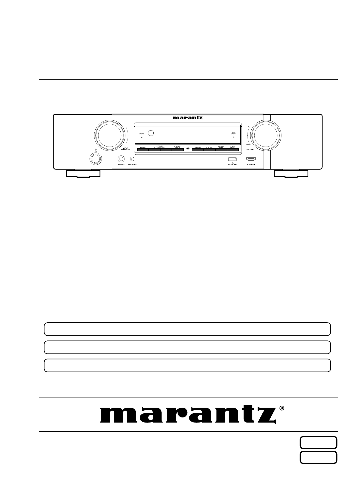
Marantz NR1506 /U1B User manual

AV SURROUND RECEIVER
NR1506 /U1B/N1B/N1SG/K1B
NR1506
S1214V03DM/DG1603
Copyright 2016 D&M Holdings Inc. All rights reserved.
WARNING: Violators will be prosecuted to the maximum extent possible.
Ver. 3
•Some illustrations using in this service manual are slightly different from the actual set.
•Please use this service manual with referring to the operating instructions without fail.
•For purposes of improvement, specications and design are subject to change without notice.
Please refer to the
MODIFICATION NOTICE.
Service
Manual

Contents
ABOUT THIS MANUAL................................................................3
What you can do with this manual ...........................................3
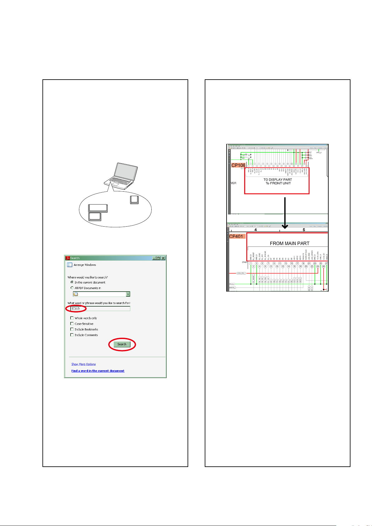
Using Adobe Reader (Windows version)...................................4
SAFETY PRECAUTIONS...............................................................6
NOTE FOR SCHEMATIC DIAGRAM..............................................7
NOTE FOR PARTS LIST................................................................7
INSTRUCTIONS
FOR HANDLING SEMI-CONDUCTORS AND OPTICAL UNIT........7
1. Ground for Human Body......................................................7
2. Ground for Workbench ........................................................7
SPECIFICATIONS ........................................................................9
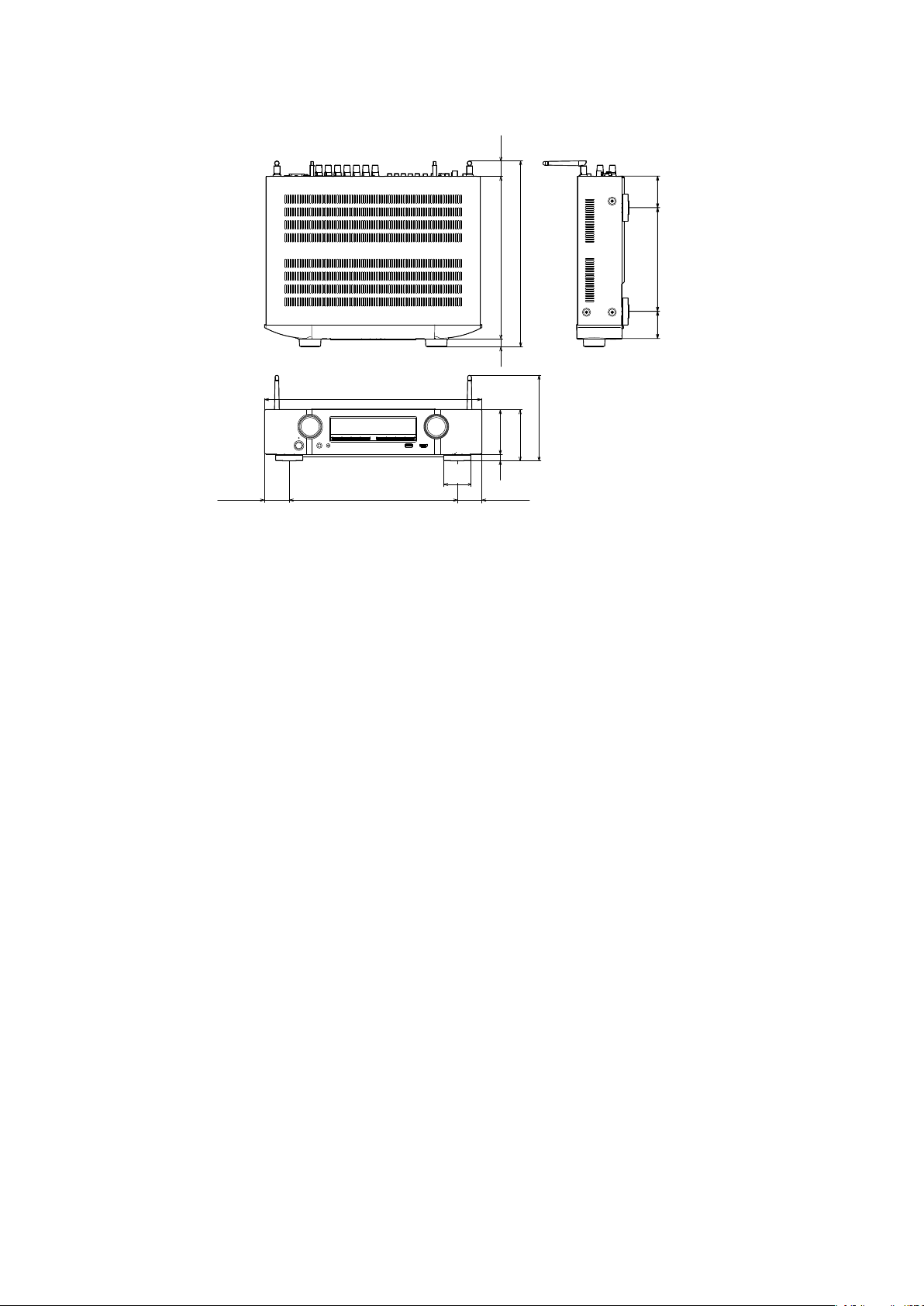
DIMENSION ..............................................................................10
CAUTION IN SERVICING ...........................................................11
Initializing This Unit.................................................................11
JIG FOR SERVICING ..................................................................11
DISASSEMBLY ..........................................................................12
1. FRONT PANEL ASSY............................................................14
2. RADIATOR ASSY .................................................................14
3. HDMI PCB...........................................................................15
4. SPK PCB..............................................................................15
5. TRANS ................................................................................16
6. SMPS PCB...........................................................................16
7. REG PCB..............................................................................16
8. AV PCB ...............................................................................16
SPECIAL MODE.........................................................................17
Special mode setting button ..................................................17
1. Version Display Mode ........................................................18
2. PANEL / REMOTE LOCK Selection Mode ............................22
3. Selecting the Mode for Service-related Operations...........23
DIAGNOSTIC PATH DIAGRAM ............................................26
4. Protection Pass Mode ........................................................44
5. CY920 Reboot Mode ..........................................................44
6. CY920 Initialization Mode ..................................................45
JIG FOR SERVICING ..................................................................46
PROCEDURE AFTER REPLACING
THE MICROPROCESSOR, ETC...................................................48
FIRMWARE UPDATE PROCEDURE............................................49
1. Updating via USB ...............................................................49
2. Updating via DPMS ............................................................58
ADJUSTMENT...........................................................................65
SURROUND MODES AND PARAMETERS..................................66
TROUBLE SHOOTING................................................................68
1. POWER ...............................................................................68
2. Analog video......................................................................69
3. HDMI/DVI ...........................................................................70
4. AUDIO ................................................................................72
5. Network / Bluetooth / USB.................................................75
6. SMPS ..................................................................................80
CLOCK FLOW & WAVE FORM IN DIGITAL BLOCK.....................82
LEVEL DIAGRAM.......................................................................83
BLOCK DIAGRAM .....................................................................87
POWER DIAGRAM ....................................................................90
WIRING DIAGRAM....................................................................91
PRINTED Circuit BOARDS.........................................................92
SCHEMATIC DIAGRAMS (1/23).................................................97
01-FRONT HDMI ......................................................................97
02-MN864788A .......................................................................98
03-NET_MN864788 .................................................................99
04-ADV7623 ..........................................................................100
05-CPU ..................................................................................101
06-CPU LEVEL CHG................................................................102
07-DIGITAL CNT.....................................................................103
08-DIR A.PLD .........................................................................104
09-MAIN DAC ........................................................................105
10-DSP...................................................................................106
11-NET PHY ...........................................................................107
12-D.SUPPLY .........................................................................108
13-SPK...................................................................................109
14-CNT ..................................................................................110
15-INPUT ............................................................................... 111
16-VIDEO...............................................................................112
17-TUNER ..............................................................................113
18-FRONT..............................................................................114
19-AMP1................................................................................115
20-AMP2................................................................................116
21-SMPS ................................................................................117
22-REG...................................................................................118
23-FRONT CNT.......................................................................119
EXPLODED VIEW ....................................................................121
PACKING VIEW .......................................................................122
SEMICONDUCTORS ................................................................123
1. IC's....................................................................................123
2. FL DISPLAY.......................................................................137
2

Jump to the target of a schematic
diagram connector
Click the Ref. No. of the target connector in the red
box around a schematic diagram connector.
•The screen jumps to the target connector.
•Pagemagnicationstaysthesameasbeforethe
jump.
CP401
CP106
v
ABOUT THIS MANUAL
Readthefollowinginformationbeforeusingtheservicemanual.
What you can do with this manual
Search for a Ref. No. (phrase)
(Ctrl+Shift+F)
YoucanusethesearchfunctioninAcrobatReaderto
searchforaRef.No.inschematicdiagrams,printed
wiringcircuitdiagrams,blockdiagrams,andparts
lists.
1.PressCtrl+Shift+Fonthekeyboard.
• TheSearchwindowappears.
2.EntertheRef.No.youwanttosearchforinthe
Searchwindow,andthenclicktheSearchbutton.
•Alistofsearchresultsappears.
3.Clickanitemonthelist.
•Thescreenjumpstothepageforthatitem,andthe
searchphraseisdisplayed.
Ctrl
Shift
F
3

Using Adobe Reader (Windows version)
• Properties
Clickthisbuttonandcheckthattheprinterissettoa
suitablepapersize.
• Page to print
Selectthefollowingcheckbox.
"More Options":"Current View"
• Page Sizing & Handling
Selectthefollowingcheckbox.
"Size"/"Size Options" :"Fit"
Add notes to this data (Sign)
TheSignfunctionletsyouaddnotestothedatain
thismanual.
Savetheleonceyouhavenishedaddingnotes.
[Example using Adobe Reader X]
Onthe"View"menu,click"Sign".
• TheSignpaneappears.
[Example using Adobe Reader 9]
Onthe "Document"menu,click"Sign".
Magnify schematic / printed circuit board
diagrams - 1
(Ctrl+Space, mouse operation)
PressCtrl+Space onthekeyboardanddragthe
mousetoselecttheareayouwanttoview.
• Theselectedareaismagnied.
• Whenyouwanttomovetheareashown,hold
downSpaceanddragthemouse.
• Whenyouwanttoshowafullpageview,press
Ctrl+0onthekeyboard.
Ctrl Space
0
Print a magnied part of the manual
ThePropertiesdialogboxandfunctionswillvarydependingonyourprinter.
1. Dragthemousetomagnifythepartyouwanttoprint.
2. Onthe"File"menu,click"Print".
3. CongurethefollowingsettingsinthePrintdialog
box.
4. ClickthePrintbuttontostartprinting.
4

Magnify schematic / printed circuit board
diagrams - 2
(Pan & Zoom function)
ThePan&Zoomfunctionletsyouseewhichpartof
amagnieddiagramisbeingshowninaseparate
window.
[Example using Adobe Reader X]
Onthe"View"menu,pointto"Zoom",andthenclick
"Pan & Zoom".
• ThePan&Zoomwindowappearsonthescreen.
[Example using Adobe Reader 9]
Onthe"Tools"menu,pointto "Select & Zoom",and
thenclick"Pan & Zoom Window".
Magnify schematic / printed circuit board
diagrams - 3
(Loupe Tool function)
TheLoupeToolfunctionletsyoumagnifyaspecic
partofadiagraminaseparatewindow.
[ExampleusingAdobeReaderX]
Onthe"View"menu,pointto"Zoom",andthenclick
"Loupe Tool".
• TheLoupeToolwindowappearsonthescreen.
[Example using Adobe Reader 9]
Onthe"Tools"menu,pointto"Select & Zoom",and
thenclick"Loupe Tool Window".
5

SAFETY PRECAUTIONS
The following items should be checked for continued protection of the customer and the service technician.
leakage current check
Before returning the set to the customer, be sure to carry out either (1) a leakage current check or (2) a line to chassis
resistance check. If the leakage current exceeds 0.5 milliamps, or if the resistance from chassis to either side of the
power cord is less than 460 kohms, the set is defective.
Be sure to test for leakage current with the AC plug in both polarities, in addition, when the set's power is in each state
(on, off and standby mode), if applicable.
CAUTION Please heed the following cautions and instructions during servicing and
inspection.
◎Heed the cautions!
Cautions which are delicate in particular for servicing
are labeled on the cabinets, the parts and the chassis,
etc. Be sure to heed these cautions and the cautions
described in the handling instructions.
◎Cautions concerning electric shock!
(1) An AC voltage is impressed on this set, so if you
touch internal metal parts when the set is energized,
you may get an electric shock. Avoid getting an
electric shock, by using an isolating transformer
and wearing gloves when servicing while the set is
energized, or by unplugging the power cord when
replacing parts, for example.
(2) There are high voltage parts inside. Handle with
extra care when the set is energized.
◎Caution concerning disassembly and
assembly!
Through great care is taken when parts were
manufactured from sheet metal, there may be burrs on
the edges of parts. The burrs could cause injury if ngers
are moved across them in some rare cases. Wear gloves
to protect your hands.
◎Use only designated parts!
The set's parts have specic safety properties (re
resistance, voltage resistance, etc.). Be sure to use parts
which have the same properties for replacement. The
burrs have the same properties. In particular, for the
important safety parts that are indicated by the zmark
on schematic diagrams and parts lists, be sure to use
the designated parts.
◎Be sure to mount parts and arrange the wires
as they were originally placed!
For safety seasons, some parts use tapes, tubes or other
insulating materials, and some parts are mounted away
from the surface of printed circuit boards. Care is also
taken with the positions of the wires by arranging them
and using clamps to keep them away from heating and
high voltage parts, so be sure to set everything back as
it was originally placed.
◎Make a safety check after servicing!
Check that all screws, parts and wires removed or
disconnected when servicing have been put back in their
original positions, check that no serviced parts have
deteriorate the area around. Then make an insulation
check on the external metal connectors and between
the blades of the power plug, and otherwise check that
safety is ensured.
(Insulation check procedure)
Unplug the power cord from the power outlet, disconnect
the antenna, plugs, etc., and on the power. Using a 500V
insulation resistance tester, check that the insulation
resistance value between the inplug and the externally
exposed metal parts (antenna terminal, headphones
terminal, input terminal, etc.) is 1MΩ or greater. If it is
less, the set must be inspected and repaired.
Many of the electric and the structural parts used in the
set have special safety properties. In most cases these
properties are difcult to distinguish by sight, and the use
of replacement parts with higher ratings (rated power
and withstand voltage) does not necessarily guarantee
that safety performance will be preserved. Parts with
safety properties are indicated as shown below on the
wiring diagrams and the parts list in this service manual.
Be sure to replace them with the parts which have the
designated part number.
(1) Schematic diagrams.......Indicated by the z mark.
(2) Parts lists.......Indicated by the zmark.
The use of parts other than the
designated parts could cause electric
shocks, res or other dangerous
situations.
CAUTION Concerning important
safety parts
6

NOTE FOR SCHEMATIC DIAGRAM
WARNING:
Parts indicated by the zmark have critical characteristics. Use ONLY replacement parts recommended by the manufacturer.
CAUTION:
Before returning the set to the customer, be sure to carry out either (1) a leakage current check or (2) a line to chassis resistance check.
If the leakage current exceeds 0.5 milliamps, or if the resistance from chassis to either side of the power cord is less than 460 kohms, the
set is defective.
WARNING:
DO NOT return the set to the customer unless the problem is identied and remedied.
NOTICE:
ALL RESISTANCE VALUES IN OHM. k=1,000 OHM / M=1,000,000 OHM
ALL CAPACITANCE VALUES ARE EXPRESSED IN MICRO FARAD, UNLESS OTHERWISE INDICATED. P INDICATES MICRO-MICRO
FARAD. EACH VOLTAGE AND CURRENT ARE MEASURED AT NO SIGNAL INPUT CONDITION. CIRCUIT AND PARTS ARE SUBJECT
TO CHANGE WITHOUT PRIOR NOTICE.
NOTE FOR PARTS LIST
1. Parts indicated by "nsp" on this table cannot be supplied.
2. When ordering a part, make a clear distinction between "1" and "I" (i) to avoid mis-supplying.
3. A part ordered without specifying its part number can not be supplied.
4. Part indicated by " ★" mark is not illustrated in the exploded view.
WARNING: Parts indicated by the zmark have critical characteristics. Use ONLY replacement parts recommended by the manufacturer.
INSTRUCTIONS FOR HANDLING SEMI-CONDUCTORS AND OPTICAL UNIT
Electrostatic breakdown of the semi-conductors or optical pickup may occur due to a potential difference caused by
electrostatic charge during unpacking or repair work.
1. Ground for Human Body
Be sure to wear a grounding band (1 MΩ) that is properly grounded to remove any static electricity that may be
charged on the body.
2. Ground for Workbench
Be sure to place a conductive sheet or copper plate with proper grounding (1 MΩ) on the workbench or other surface,
where the semi-conductors are to be placed. Because the static electricity charge on clothing will not escape through
the body grounding band, be careful to avoid contacting semi-conductors with your clothing
<Incorrect>
CBA
Grounding Band
Conductive Sheet or
Copper Plate
1MΩ
1MΩ
<Correct>
CBA
7

8
Personal notes:

n
50 W + 50 W (8 Ω, 20 Hz – 20 kHz with 0.08 % T.H.D.)
60 W + 60 W (6 Ω, 1 kHz with 0.7 % T.H.D.)
50 W (8 Ω, 20 Hz – 20 kHz with 0.08 % T.H.D.)
60 W (6 Ω, 1 kHz with 0.7 % T.H.D.)
50 W + 50 W (8 Ω, 20 Hz – 20 kHz with 0.08 % T.H.D.)
60 W + 60 W (6 Ω, 1 kHz with 0.7 % T.H.D.)
4 – 16 Ω
n
130 mV / 47 kΩ
10 Hz – 100 kHz — +1, –3 dB (Direct mode)
98 dB(IHF-A, weighted, Direct mode)
n
1 Vp-p, 75 Ω
5 Hz - 10 MHz — 0, -3 dB
n
(Note : μV at 75 Ω, 0 dBf = 1 x 10 –15 W)
87.5 MHz - 107.9 MHz (for U)
87.5 MHz - 108.0 MHz (for N, K)
520 kHz - 1710 kHz (for U)
522 kHz - 1611 kHz (for N, K)
1.2 μV (12.8 dBf)
18 μV
MONO―2.8μV(20.2dBf)
MONO ― 70 dB (IHF-A weighted, Direct mode)
STEREO ― 67 dB (IHF-A weighted, Direct mode)
MONO ― 0.7 % (1 kHz)
SRETEO ― 1.0 % (1 kHz)
n
Conforming to IEEE 802.11b
Conforming to IEEE 802.11g
Conforming to IEEE 802.11n
(Wi-Fi® compliant)z1
WEP 64 bit, WEP 128 bit
WPA/WPA2-PSK (AES)
WPA/WPA2-PSK (TKIP)
2.4 GHz
1 - 11 ch (for U)
1 - 13 ch (for N, K)
z1 The Wi-Fi® CERTIFIED Logo and the Wi-Fi CERTIFIED On-Product Logo
are registered trademarks of the Wi-Fi Alliance.
n
Bluetooth Version 2.1 + EDR
(Enhanced Data Rate)
Maximum2.5 mW (Class 2)
Approx. 32.8 ft/10 m in line of sightz2
2.4 GHz band
FHSS (Frequency-Hopping Spread
Spectrum)
A2DP (Advanced Audio Distribution Prole) 1.2
AVRCP (Audio Video Remote Control Prole) 1.4
SBC, AAC
20Hz-20,000Hz
z2 The actual communication range varies depending on the inuence of
such factors as obstructions between devices, electromagnetic waves
from microwave ovens, static electricity, cordless phones, reception
sensitivity, antenna performance, operating system, application
software etc.
n
(for U) : AC 120 V, 60 Hz
(for N) : AC 230 V, 50 Hz / 60 Hz
(for K) : AC 220 V, 50 Hz
180 W
0.2 W
0.5 W
2.7 W
For purposes of improvement, specications and design are subject to
change without notice.
9

17 5/16 (440)
2 3/16
(55) 2 1/2
(63)
9/16
(14)
13 3/8 (340)
2 3/16
(55)
1 15/16 (50)1 15/16 (50)
5/8
(16)
1 1/4
(32)
8 1/4 (210)
12 15/16 (328)
14 13/16 (376)
3 9/16
(91)
4 1/8 (105)
6 13/16 (173)
DIMENSION
Unit : in. (mm)
Weight : 18 lbs 1 oz (8.2 kg)
10

CAUTION IN SERVICING
Initializing This Unit
Make sure to initialize this unit after replacing the microcomputer or any peripheral equipment, or the digital PCB.
1. Press the power button to turn off the power.
2. While holding down buttons "TUNER PRESET CH +" and "INTERNET RADIO" simultaneously, press the power but-
ton to turn on the power.
3. Release the buttons after conrming that the display ashes at 1-second intervals.
* The unit is initialized.
NOTE:• If the unit fails to enter the service mode in step 3, repeat the procedure from step 1.
• Initializing the device restores the customized settings to the factory settings. Write down your settings in advance and
recongure the settings after initialization.
JIG FOR SERVICING
Use the following jigs (extension cable kit) when repairing the PCBs.
Order with your dealer for the jigs your dealer if necessary.
8U-110084S : EXTENSION UNIT KIT : 1Set
8U-110136S : EXTENSION UNIT KIT : 1Set
(See page 46)
INTERNET RADIOPRESET CH +POWER
11

FRONT PANEL ASSY
See "DISASSEMBLY"
1. FRONT PANEL ASSY
and "EXPLODED VIEW"
FRONT PCB
Ref. No. of EXPLODED VIEW : 14
HP PCB
Ref. No. of EXPLODED VIEW : 9
USB PCB
Ref. No. of EXPLODED VIEW : 42
FRONT-HDMI PCB
Ref. No. of EXPLODED VIEW : 12
HDMI_GUIDE_B PCB
Ref. No. of EXPLODED VIEW : 15
HDMI_GUIDE_A PCB
Ref. No. of EXPLODED VIEW : 16
TOP COVER
REG PCB
See "DISASSEMBLY"
7. REG PCB
and "EXPLODED VIEW"
REG PCB
Ref. No. of EXPLODED VIEW : 40
AV PCB
See "DISASSEMBLY"
8. AV PCB
and "EXPLODED VIEW"
AV PCB
Ref. No. of EXPLODED VIEW : 45
FRONT_CNT PCB
Ref. No. of EXPLODED VIEW : 43
SIDE_CNT PCB
Ref. No. of EXPLODED VIEW : 46
RADIATOR ASSY
See "DISASSEMBLY"
2. RADIATOR ASSY
and "EXPLODED VIEW"
5CH_AMP PCB
Ref. No. of EXPLODED VIEW : 24
GUIDE_L PCB
Ref. No. of EXPLODED VIEW : 18
HDMI PCB
See "DISASSEMBLY"
3. HDMI PCB
and "EXPLODED VIEW"
HDMI PCB
Ref. No. of EXPLODED VIEW : 47
CY920, MODULE
Ref. No. of EXPLODED VIEW : 57
TRANS
See "DISASSEMBLY"
5. TRANS
and "EXPLODED VIEW"
POWER TRANS
Ref. No. of EXPLODED VIEW : 31
SMPS PCB
See "DISASSEMBLY"
6. SMPS PCB
and "EXPLODED VIEW"
SMPS PCB
Ref. No. of EXPLODED VIEW : 37
SPK PCB
See "DISASSEMBLY"
4. SPK PCB
and "EXPLODED VIEW"
SPK PCB
Ref. No. of EXPLODED VIEW : 38
DISASSEMBLY
• Remove each part following the ow below.
• Reassemble the removed parts in the reverse order.
• Read "Precautions During Work" before reassembling the removed parts.
• If wire bundles are removed or moved during adjustment or part replacement, reshape the wires after completing
the work. Failure to shape the wires correctly may cause problems such as noise.
12

Explanatory Photos for DISASSEMBLY
• For the shooting direction of each photos used in this manual, see the photo below.
• A, B, C and D in the photo below indicate the shooting directions of photos.
• The photographs with no shooting direction indicated were taken from the top of the unit.
• Photos of NR1506 K1B are used in this manual.
The viewpoint of each photograph
(Shooting direction : X) [View from the top]
↑Shooting direction: A↑
↓Shooting direction: B↓
↓Shooting direction: D↓
↑Shooting direction: C↑
Front side
s
13

1. FRONT PANEL ASSY
Proceeding : TOP COVER →FRONT PANEL ASSY
(1) Remove the screws.
(2) Remove the screws. Remove the CORD HOLDERs and connector wires. Remove the FFC.
2. RADIATOR ASSY
Proceeding : TOP COVER →RADIATOR ASSY
(1) Remove the screws.
(2) Remove the screws. Cut the wire clamp, then remove the connector. Remove the FFC.
View from the bottom
x4
x1 x1
FFC
FFC
N1023
CP4401
x4
CORD HOLDER
View from the bottom
x7
x4
N1023
FFC FFC
CP4802
CP4800
CP4401
CP4801
CORD HOLDERx3
CUT
s
s
14

3. HDMI PCB
Proceeding : TOP COVER →HDMI PCB
(1) Remove the screws.
(2) Remove the CORD HOLDERs. Cut the wire clamp, then remove the connector. Remove the FFC.
4. SPK PCB
Proceeding : TOP COVER →DIGITAL PCB →SPK PCB
(1) Remove the screws.
(2) Remove the screws. Remove the CORD HOLDERs and connector wires.
Shooting direction: A
x6
x2
FFC FFC
N1023
N1021
N1006 N1005
CORD HOLDER
N1001
N1003
N1002
CORD HOLDER x 3
CUT
CUT
Shooting direction: A
x3
x5
x1
CP4802
CP4000
CP4002
CP4801
CORD HOLDERx4
s
15

5. TRANS
Proceeding : TOP COVER →DIGITAL PCB →TRANS
(1) Remove the CORD HOLDERs and connector wires.
(2) Remove the screws.
NOTE : It will separate and TRANS will fall from SET, if screws is removed.
6. SMPS PCB
Proceeding : TOP COVER →SMPS PCB
See "EXPLODED VIEW" for instructions on removing the SMPS PCB.
7. REG PCB
Proceeding : TOP COVER →REG PCB
See "EXPLODED VIEW" for instructions on removing the REG PCB.
8. AV PCB
Proceeding : TOP COVER →AV PCB
See "EXPLODED VIEW" for instructions on removing the AV PCB.
CP4001
CP4401
CP4607
CP4142
CORD HOLDERx5
View from the bottom
x4
16

SPECIAL MODE
Special mode setting button
b No. 1 - 6, 9 : While holding down buttons "A", "B" and "C" simultaneously, press the power button to turn on the power.
b No. 7, 8 : While the power is on, hold down buttons "A" and "B" for at least 3 seconds .
b No. 10 : While holding down buttons "A" and "B" simultaneously, insert the AC plug into the wall outlet to turn on the power.
No. Mode Button A Button B Button C Descriptions
1Version Display
(u-COM / DSP Error Display) DIMMER STATUS –
Displays the version of rmware such as the main rmware or
DSP. Errors that have occurred are displayed.
(See page 18)
2Selecting the Mode for Service-related PRESET
CH + STATUS - This is a display for turning on each service-related mode.
Service-related modes: No. 2-1 - No. 2-5
2-1 Protection history display mode ↑ ↑ - Displays the protection occurrence history.
(See page 40)
2-2 Check the Video/Audio path Mode ↑ ↑ -
This is a special mode for service conrmation used during
repair work to simplify the conrmation work for the Audio
channel / video channel.
(See page 23)
2-3 TUNER STEP Mode
(U and N model only) ↑ ↑ - Enables reception STEP of the ANALOG TUNER to be changed.
(See page 43)
2-4 Operation Info Mode ↑ ↑ -
Displays the accumulated operating time of the unit, the num-
ber of times the power was switched on, and the number of
occurrences of each protection.
(See page 42)
3User Initialization Mode M-DAX PRESET
CH + -Initializes backup data.
(Settings for the Installer Setup are not initialized.)
4Factory Initialization Mode PRESET
CH +
INTERNET
RADIO -Initializes backup data.
(The settings for the Installer Setup is also initialized.)
5PANEL / REMOTE LOCK Selection Mode M-DAX DIMMER -
Start this unit in the PANEL/REMOTE LOCK selection mode so
that PANEL LOCK and Remote Lock can be switched between
ON and OFF.
(See page 22)
6Protection Pass Mode DIMMER STATUS SOUND
MODE
Enables the power to be turned on when protection detection
is disabled.
(See page 44)
7CY920 Reboot Mode DIMMER SOUND
MODE -Reboot CY920.(See page 44)
8CY920 Initialization Mode DIMMER STATUS -
Enter this mode only after replacing Flash for CY920 and rewrit-
ing the rmware.
(See page 45)
9USB Update Mode DIMMER SOUND
MODE -Switches this unit to USB Update mode.
(See page 49)
10 Forced USB All Device Write Mode DIMMER SOUND
MODE -
Mode used when this unit cannot be recovered.
Forcibly switches this unit to USB update mode.
(See page 51)
PRESET CH +PRESET CH -
INTERNET RADIO
M-DAX
STATUS
DIMMER
SOUND MODE
POWER
17

1. Version Display Mode
1.1. Actions
Version information is displayed when the device is started in this mode.
1.2. Starting up
While holding down buttons "DIMMER" and "STATUS" simultaneously, press the power button to turn on the power.
then press the "STATUS" button to display the information in section 1.3 on the display.
b The version list is also displayed on GUI while the version is displayed on the display.
1.3. Display Order
q Firmware Package Version → w Firmware Package Version
→ e Main µ-com → r Main 1st Boot Loader → t DSP ROM → y Audio PLD → u GUI SFLASH
→ i Ethernet 1st Boot Loader, Hardware ID → o Ethernet 2nd Boot Loader, Rhapsody Flag
→ Q0 Ethernet IMAGE → Q1 Ethernet MAC ADDRESS information → Q2 BT MAC ADDRESS information
q Model destination information :
FLD N R 1 5 0 6 U *
FLD N R 1 5 0 6 N *
FLD N R 1 5 0 6 K *
w Firmware Package Version:
FLD Package :****
e Main µ-com Version information :
FLD Main :****####*
*
: Main version, #: Sub version
r Main 1st Boot Loader :
FLD Main FBL :**.**
t DSP ROM :
FLD DSP :**.**
y Audio PLD :
FLD Audio PLD:**.**
u GUI SFLASH :
FLD GUI :@@$\****
@
: Model code, $
: Brand code, \
: Region code, *
: version
18

i Ethernet 1st Boot Loader, Hardware ID :
FLD Ethernet FBL
Press "STATUS" button.
FLD ******-bd
o Ethernet 2nd Boot Loader, Rhapsody Flag :
FLD Ethernet SBL
Press "STATUS" button.
FLD B************-0A
Q0 Ethernet IMAGE :
FLD Ethernet IMG
Press "STATUS" button.
FLD I************
Q1 Ethernet MAC ADDRESS information:
FLD * N E T M A C A d d r e s s
Press "STATUS" button.
FLD ******-******
Q2 BT MAC ADDRESS information:
FLD *BT MAC Address
Press "STATUS" button.
FLD ******-******
19

1.4. Error display
See the table below for descriptions of the displayed errors and countermeasures for these.
If multiple errors occur, only one item is displayed.
The priority order is w, e, r, t, q.
Condition States Display TROUBLE SHOOTING
q
Firm Check
NG
The model name, brand name and region
information written in the rmware are
compared to the region settings in the
PCB. This error is displayed if the informa-
tion does not match.
" ▲ " or " ▼ " is displayed as the rst char-
acter if the rmware is not correct (see the
illustrations on the right).
FIRM ERROR
–
Main :********
–
DSP :**.**
–
Audio PLD:**.**
–
GUI :********
• Check the resistor
for setting the re-
gion(R1202 / R1206,
HDMI PCB).
• Write the rmware for
the correct region.
w
GUI Serial
Flash NG
If the Main CPU version is not supported
by the GUI Serial Flash ," ▼ " is displayed
as the rst character of the GUI rmware
version.
GUI VER. ERROR
•
GUI :********
• Check the rmware
version.
e
DIR NG
This error is displayed if there is no re-
sponse from the DIR. DIR ERROR 01
• Check the DIR (U1016,
HDMI PCB) and sur-
rounding circuits.
r
DSP NG
The DSP FLAG0 port does not enter "Hi"
status while booting a DSP code even
after resetting DSP.
DSP ERROR 01
• Check the DSP (U1021,
HDMI PCB) and sur-
rounding circuits.
The DSP FLAG0 port does not enter "Hi"
status before issuing a DSP command. DSP ERROR 02
Setting WRITE to "Lo" does not set ACK to
"Hi" during DSP data reading. DSP ERROR 03
Setting REQ to "Lo" does not set ACK to
"Lo" during DSP data reading. DSP ERROR 04
Setting WRITE to "Hi" does not set ACK to
"Hi" during DSP data writing. DSP ERROR 05
Setting REQ to "Lo" does not set ACK to
"Lo" during DSP data writing. DSP ERROR 06
t
EEPROM NG
An error occurred in a checksum of the
EEPROM(*** is a block address number). E2PROM ERR***
20
This manual suits for next models
3
Table of contents
Other Marantz Stereo Receiver manuals

Marantz
Marantz SR9600 User manual

Marantz
Marantz 2250B User manual

Marantz
Marantz 2285B User manual

Marantz
Marantz 4270 User manual

Marantz
Marantz SR7007 User manual

Marantz
Marantz 2285 User manual

Marantz
Marantz SR5007 User manual

Marantz
Marantz SR6003 User manual

Marantz
Marantz SR-63 User manual

Marantz
Marantz SR8500 User manual

Marantz
Marantz 2215 User manual

Marantz
Marantz SR-4320 User manual

Marantz
Marantz SR8200 User manual

Marantz
Marantz SR7300 User manual

Marantz
Marantz 2270 User manual

Marantz
Marantz SR7010 User manual

Marantz
Marantz SR5008 User manual

Marantz
Marantz 4230 User manual

Marantz
Marantz 2275 User manual

Marantz
Marantz SR4003 User manual