Marvell 88E3016 User manual

Marvell. Moving Forward Faster
Doc. No. MV-S103164-00, Rev. A
January 4, 2008
Document Classification: Proprietary Information
88E3016
Integrated 10/100 Fast Ethernet Transceiver

Document Status
Advance
Information
This document contains design specifications for initial product development. Specifications may
change without notice. Contact Marvell Field Application Engineers for more information.
Preliminary
Information
This document contains preliminary data, and a revision of this document will be published at a later
date. Specifications may change without notice. Contact Marvell Field Application Engineers for
more information.
Final
Information
This document contains specifications on a product that is in final release. Specifications may
change without notice. Contact Marvell Field Application Engineers for more information.
Revision Code: Rev. A
Advance Technical Publication: 1.10
Document Conventions
Note: Provides related information or information of special importance.
Caution: Indicates potential damage to hardware or software, or loss of data.
Warning: Indicates a risk of personal injury.
For more information, visit our website at: www.marvell.com
Disclaimer
No part of this document may be reproduced or transmitted in any form or by any means, electronic or mechanical, including photocopying and recording, for any purpose,
without the express written permission of Marvell. Marvell retains the right to make changes to this document at any time, without notice. Marvell makes no warranty of any
kind, expressed or implied, with regard to any information contained in this document, including, but not limited to, the implied warranties of merchantability or fitness for any
particular purpose. Further, Marvell does not warrant the accuracy or completeness of the information, text, graphics, or other items contained within this document.
Marvell products are not designed for use in life-support equipment or applications that would cause a life-threatening situation if any such products failed. Do not use
Marvell products in these types of equipment or applications.
With respect to the products described herein, the user or recipient, in the absence of appropriate U.S. government authorization, agrees:
1) Not to re-export or release any such information consisting of technology, software or source code controlled for national security reasons by the U.S. Export Control
Regulations ("EAR"), to a national of EAR Country Groups D:1 or E:2;
2) Not to export the direct product of such technology or such software, to EAR Country Groups D:1 or E:2, if such technology or software and direct products thereof are
controlled for national security reasons by the EAR; and,
3) In the case of technology controlled for national security reasons under the EAR where the direct product of the technology is a complete plant or component of a plant,
not to export to EAR Country Groups D:1 or E:2 the direct product of the plant or major component thereof, if such direct product is controlled for national security reasons
by the EAR, or is subject to controls under the U.S. Munitions List ("USML").
At all times hereunder, the recipient of any such information agrees that they shall be deemed to have manually signed this document in connection with their receipt of any
such information.
Copyright © 2008. Marvell International Ltd. All rights reserved. Marvell, the Marvell logo, Moving Forward Faster, Alaska, Fastwriter, Datacom Systems on Silicon, Libertas,
Link Street, NetGX, PHYAdvantage, Prestera, Raising The Technology Bar, The Technology Within, Virtual Cable Tester, and Yukon are registered trademarks of Marvell.
Ants, AnyVoltage, Discovery, DSP Switcher, Feroceon, GalNet, GalTis, Horizon, Marvell Makes It All Possible, RADLAN, UniMAC, and VCT are trademarks of Marvell. All
other trademarks are the property of their respective owners.
88E3016
Integrated 10/100 Fast Ethernet Transceiver
Doc. No. MV-S103164-00 Rev. A Copyright © 2008 Marvell
Page 2 Document Classification: Proprietary Information January 4, 2008, Advance
88E3016
Integrated 10/100 Fast Ethernet Transceiver
Copyright © 2008 Marvell Doc. No. MV-S103164-00, Rev. A
January 4, 2008, Advance Document Classification: Proprietary Information Page 3
OVERVIEW
The Marvell® 88E3016 device is the fourth generation
Marvell®DSP-based physical layer transceiver for
Fast Ethernet applications. The device contains all the
active circuitry to convert data streams to and from a
Media Access Controller (MAC) and the physical
media. The 88E3016 device incorporates IEEE 802.3u
Auto-Negotiation in support of both 100BASE-TX and
10BASE-T networks over twisted-pair cable in full-
duplex or half-duplex mode.
The 88E3016 device supports the Reduced Gigabit
Media Independent Interface (RGMII).
The 88E3016 device features a mode of operation
supporting IEEE compliant 100BASE-FX fiber-optic
networks. Additionally, the 88E3016 device imple-
ments Far-End Fault Indication (FEFI) in order to pro-
vide a mechanism for transferring information from the
local station to the link partner that indicates a remote
fault has occurred in 100BASE-FX mode.
The 88E3016 device features the Marvell Virtual Cable
Tester ®(VCT™) technology, which enables IT manag-
ers and networking equipment manufacturers to
remotely analyze the quality and characteristics of the
attached cable plant.
The 88E3016 device uses advanced mixed-signal pro-
cessing and power management techniques for
extremely low power dissipation and high port count
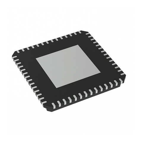
system integration. The 88E3016 device is manufac-
tured in an all CMOS process and packaged in a 64-
pin QFN package.
FEATURES
•IEEE 802.3 compliant 100BASE-TX and
10BASE-T ports
•Reduced Gigabit Media Independent Interface
(RGMII)
•Virtual Cable Tester®(VCT™) Technology
•PECL interface supporting 100BASE-FX applica-
tions
•Automatic MDI/MDIX crossover for 10BASE-T
and 100BASE-TX
•Jumbo frame support to 10 Kbytes with up to
±150 ppm clock frequency difference
•IEEE 802.3u Auto-Negotiation support for auto-
matic speed and duplex selection
•Far-End Fault Indication (FEFI) support for
100BASE-FX applications
•Supports 802.3ah Unidirectional Enable
•Energy detect feature
•Baseline wander correction
•Auto-Calibration for MAC Interface outputs
•COMA Mode support
•Flexible serial management interface (MDC/
MDIO) for register access
•Programmable interrupt to minimize polling
•IEEE 1149.1 Standard Test Access Port and
boundary scan compatible
•Supports three (3) LEDs per port
•0.15 μm standard digital CMOS process
•64-pin QFN 9 mm x 9 mm package

88E3016
Integrated 10/100 Fast Ethernet Transceiver
Doc. No. MV-S103164-00, Rev. A Copyright © 2008 Marvell
Page 4 Document Classification: Proprietary Information January 4, 2008, Advance
88E3016 Device Functional Block Diagram
MDIP/N[1]
MDIP/N[0]
SIGDET
Auto MDIX
Crossover
DAC
ADC
Digital
Adaptive
Equalizer
Baseline
Wander
Canceller
10 Mbps
Receiver 10/100
Mbps
Receive
PCS
10/100
Mbps
Transmit
PCS
FX Link
& Auto
Negotiation
RGMII
RXD[3:0]
RX_CTRL
TX_CTRL
TXD[3:0]
Management
Interface
MDC
MDIO
LED/
Configuration
LED[2:0]
TX_CLK
RX_CLK
CONFIG[3:0]
JTAG Boundary
Scan
XTAL_IN
Clock/
Reset
XTAL_OUT
RESETn
COMAn
2.5V
Regulator
1.2V
Regulator
CTRL25
DIS_REG12
VREF

Copyright © 2008 Marvell Doc. No. MV-S103164-00, Rev. A
January 4, 2008, Advance Document Classification: Proprietary Information Page 5
Table of Contents
SECTION 1. SIGNAL DESCRIPTION ...................................................................8
1.1 88E3016 Device 64-Pin QFN Pinout ............................................................................. 8
1.2 Pin Description............................................................................................................... 9
1.2.1 Pin Type Definitions ........................................................................................................... 9
1.2.2 88E3016 64-Pin QFN Assignments - Alphabetical by Signal Name ................................ 16
SECTION 2. FUNCTIONAL DESCRIPTION..........................................................17
2.1 Reduced Gigabit Media Independent Interface (RGMII) ........................................... 18
2.2 Serial Management Interface ...................................................................................... 19
2.2.1 MDC/MDIO Read and Write Operations .......................................................................... 19
2.2.2 Preamble Suppression ..................................................................................................... 20
2.2.3 Programming Interrupts.................................................................................................... 20
2.3 Transmit and Receive Functions................................................................................ 21
2.3.1 Transmit Side Network Interface ...................................................................................... 21
2.3.2 Encoder ............................................................................................................................ 21
2.3.3 Receive Side Network Interface ....................................................................................... 21
2.3.4 Decoder............................................................................................................................ 22
2.3.5 Auto-Negotiation............................................................................................................... 23
2.4 Power Management ..................................................................................................... 24
2.4.1 IEEE Power Down Mode.................................................................................................. 24
2.4.2 Energy Detect +TM ..........................................................................................................24
2.4.3 Normal 10/100 Mbps Operation ....................................................................................... 24
2.4.4 COMA Mode..................................................................................................................... 25
2.5 Regulators and Power Supplies ................................................................................. 26
2.5.1 AVDD ............................................................................................................................... 26
2.5.2 AVDDC............................................................................................................................. 26
2.5.3 AVDDR............................................................................................................................. 26
2.5.4 AVDDX ............................................................................................................................. 27
2.5.5 DVDD ............................................................................................................................... 27
2.5.6 VDDO ............................................................................................................................... 27
2.5.7 VDDOR ............................................................................................................................ 27
2.6 Hardware Configuration .............................................................................................. 28
2.7 Far End Fault Indication (FEFI)................................................................................... 30
2.8 802.3ah Unidirectional Enable .................................................................................... 30
2.9 Virtual Cable Tester® Feature..................................................................................... 31
2.10 Auto MDI/MDIX Crossover .......................................................................................... 32

Doc. No. MV-S103164-00, Rev. A Copyright © 2008 Marvell
Page 6 Document Classification: Proprietary Information January 4, 2008, Advance
88E3016
Integrated 10/100 Fast Ethernet Transceiver
2.11 LED Interface ................................................................................................................33
2.11.1 Manual Override ............................................................................................................... 33
2.11.2 PHY Control...................................................................................................................... 34
2.11.3 LED Polarity...................................................................................................................... 38
2.11.4 Stretching and Blinking..................................................................................................... 38
2.12 Automatic and Manual Impedance Calibration..........................................................39
2.12.1 MAC Interface Calibration Circuit ..................................................................................... 39
2.12.2 MAC Interface Calibration Register Definitions ................................................................ 39
2.12.3 Changing Auto Calibration Targets .................................................................................. 40
2.12.4 Manual Settings to The Calibration Registers .................................................................. 40
2.13 CRC Error Counter .......................................................................................................44
2.13.1 Enabling The CRC Error Counter..................................................................................... 44
2.14 IEEE 1149.1 Controller ................................................................................................45
2.14.1 Bypass Instruction ............................................................................................................ 45
2.14.2 Sample/Preload Instruction .............................................................................................. 45
2.14.3 Extest Instruction .............................................................................................................. 46
2.14.4 The Clamp Instruction ...................................................................................................... 47
2.14.5 The HIGH-Z Instruction ....................................................................................................47
2.14.6 ID CODE Instruction ......................................................................................................... 47
SECTION 3. REGISTER DESCRIPTION ............................................................. 48
SECTION 4. ELECTRICAL SPECIFICATIONS ..................................................... 78
4.1. Absolute Maximum Ratings ........................................................................................78
4.2. Recommended Operating Conditions ........................................................................79
4.3 Package Thermal Information .....................................................................................80
4.3.1 88E3016 Device 64-Pin QFN package............................................................................. 80
4.4 Current Consumption ..................................................................................................81
4.4.1 Current Consumption AVDD + Center Tap ...................................................................... 81
4.4.2 Current Consumption AVDDC.......................................................................................... 81
4.4.3 Current Consumption DVDD ............................................................................................ 82
4.4.4 Current Consumption VDDO + VDDOR........................................................................... 82
4.5. DC Operating Conditions.............................................................................................83
4.5.1 Non-RGMII Digital Pins .................................................................................................... 83
4.5.2 Stub-Series Transceiver Logic (SSTL_2) ......................................................................... 84
4.5.3 IEEE DC Transceiver Parameters.................................................................................... 86
4.6 AC Electrical Specifications ........................................................................................87
4.6.1 Reset and Configuration Timing ....................................................................................... 87
4.6.2 XTAL_IN Input Clock Timing ............................................................................................ 88
4.7 RGMII Interface Timing ................................................................................................89
4.7.1 RGMII Transmit Timing .................................................................................................... 89
4.7.2 RGMII Receive Timing ..................................................................................................... 90

Copyright © 2008 Marvell Doc. No. MV-S103164-00, Rev. A
January 4, 2008, Advance Document Classification: Proprietary Information Page 7
4.8 Latency Timing............................................................................................................. 92
4.8.1 RGMII to 100BASE-TX Transmit Latency Timing ............................................................ 92
4.8.2 RGMII to 10BASE-T Transmit Latency Timing................................................................. 92
4.8.3 100BASE-TX to RGMII Receive Latency Timing ............................................................ 93
4.8.4 10BASE-T to RGMII Receive Latency Timing................................................................. 93
4.9 Serial Management Timing ......................................................................................... 94
4.10 JTAG Timing.................................................................................................................95
SECTION 5. PACKAGE MECHANICAL DIMENSIONS ..........................................96
5.1 88E3016 Package Mechanical Dimensions ............................................................... 96
SECTION 6. APPLICATION EXAMPLES.............................................................98
6.1 10BASE-T/100BASE-TX Circuit Application .............................................................. 98
6.2 FX Interface to 3.3V Fiber Transceiver....................................................................... 99
6.3 Transmitter - Receiver Diagram................................................................................ 100
6.4 88E3016 to 88E3016 Backplane Connection - 100BASE-FX Interface .................. 101
6.5 88E3016 to Another Vendor’s PHY - 100BASE-FX Interface through a Backplane102
6.6 Marvell® PHY to Marvell PHY Direct Connection ................................................... 103
SECTION 7. ORDER INFORMATION ...............................................................104
7.1 Ordering Part Numbers and Package Markings ..................................................... 104

Doc. No. MV-S103164-00, Rev. A Copyright © 2008 Marvell
Page 8 Document Classification: Proprietary Information January 4, 2008, Advance

88E3016
Integrated 10/100 Fast Ethernet Transceiver
Section 1. Signal Description
1.1 88E3016 Device 64-Pin QFN Pinout
The 88E3016 is manufactured in a 64-pin QFN.
Figure 1: 88E3016 Integrated 10BASE-T/100BASE-TX Fast Ethernet Transceiver 64-Pin QFN
Package
1
2
3
4
5
6
7
8
9
10
11
12
13
14
15
16
Top View
33
34
35
36
37
38
39
40
41
42
43
44
45
46
47
48
NC
AVDD
NC
MDIP[1]
MDIN[1]
NC
NC
NC
NC
NC
SIGDET
CTRL25
NC
MDIN[0]
MDIP[0]
TSTPT
VDDOR
RX_CLK
RXD[2]
RXD[3]
VDDOR
TXD[1]
TXD[2]
TXD[3]
TX_CTRL
CONFIG[0]
VREF
RXD[1]
RXD[0]
RX_CTRL
17
18
19
20
21
22
23
24
25
26
30
31
32
27
28
29
64
63
62
61
60
59
58
57
56
55
51
50
49
54
53
52
CONFIG[1]
CONFIG[2]
CONFIG[3]
COMAn
LED[0]
VDDO
LED[1]
LED[2]
RESETn
AVDDR
AVDDR
AVDDX
DVDD
TRSTn
DIS_REG12
DVDD
MDC
NC
VDDO
MDIO
TDI
TCK
TMS
DVDD
XTAL_OUT
HSDACN
AVDDC
RSET
TDO
XTAL_IN
NC
HSDACP
TX_CLK
TXD[0]
88E3016
EPAD - VSS

Copyright © 2008 Marvell Doc. No. MV-S103164-00, Rev. A
January 4, 2008, Advance Document Classification: Proprietary Information Page 9
Signal Description
Pin Description
1.2 Pin Description
1.2.1 Pin Type Definitions
Pin Type Definition
H Input with hysteresis
I/O Input and output
I Input only
O Output only
PU Internal pull up
PD Internal pull down
D Open drain output
Z Tri-state output
mA DC sink capability

Doc. No. MV-S103164-00, Rev. A Copyright © 2008 Marvell
Page 10 Document Classification: Proprietary Information January 4, 2008, Advance
88E3016
Integrated 10/100 Fast Ethernet Transceiver
Table 1: RGMII Interface
88E3016 Pin Name Type Description
60 TX_CLK/TXC I RGMII Transmit Clock provides a 25 MHz or 2.5 MHz reference
clock with ± 50 ppm tolerance depending on speed. In RGMII
mode, TX_CLK is used as TXC.
63 TX_CTRL/TX_CTL I RGMII Transmit Control. TX_EN is presented on the rising edge of
TX_CLK. In RGMII mode, TX_CTRL is used as TX_CTL.
A logical derivative of TX_EN and TX_ER is presented on the fall-
ing edge of TX_CLK.
62
61
59
58
TXD[3]/TD[3]
TXD[2]/TD[2]
TXD[1]/TD[1]
TXD[0]/TD[0]
I RGMII Transmit Data. In RGMII mode, TXD[3:0] are used as
TD[3:0].
The transmit data nibble is presented on TXD[3:0] on the rising
edge of TX_CLK.
53 RX_CLK/RXC O RGMII Receive Clock provides a 25 MHz or 2.5 MHz reference
clock with ± 50 ppm tolerance derived from the received data
stream depending on speed. In RGMII mode, RX_CLK is used as
RXC.
49 RX_CTRL/
RX_CTL
O RGMII Receive Control. RX_DV is presented on the rising edge of
RX_CLK. In RGMII mode, RX_CTRL is used as RX_CTL.
A logical derivative of RX_DV and RX_ER is presented on the fall-
ing edge of RX_CLK.
55
54
51
50
RXD[3]/RD[3]
RXD[2]/RD[2]
RXD[1]/RD[1]
RXD[0]/RD[0]
O RGMII Receive Data. In RGMII mode, RXD[3:0] are used as
RD[3:0].
The receive data nibble is presented on RXD[3:0] on the rising
edge of RX_CLK.

Copyright © 2008 Marvell Doc. No. MV-S103164-00, Rev. A
January 4, 2008, Advance Document Classification: Proprietary Information Page 11
Signal Description
Pin Description
Table 2: Network Interface
88E3016 Pin Name Type Description
31
30
MDIP[0]
MDIN[0]
I/O Media Dependent Interface[0].
In MDI configuration, MDI[0]± is used for the transmit pair. In MDIX
configuration, MDI[0]± is used for the receive pair.
26
25
MDIP[1]
MDIN[1]
I/O Media Dependent Interface[1].
In MDI configuration, MDI[1]± is used for the receive pair. In MDIX
configuration, MDI[1]± is used for the transmit pair.
18 SIGDET I In 100BASE-FX mode, SIGDET indicates whether a signal is
detected by the fiber optic transceiver.
In 100BASE-TX/10BASE-T modes, this pin should not be left
floating. It should be tied either high or low.
Table 3: Serial Management Interface
88E3016 Pin Name Type Description
48 MDC I MDC is the clock reference for the serial management interface. A
continuous clock stream is not required (i.e., MDC can be stopped
when the MDC/MDIO master is not sending a command). The
maximum frequency supported is 8.33 MHz.
45 MDIO I/O MDIO is the management data. MDIO is used to transfer manage-
ment data in and out of the device synchronously to MDC. This pin
requires a pull-up resistor in a range from 1.5 kohm to 10 kohm.
Table 4: LED
88E3016 Pin Name Type Description
9 LED[2]/Interrupt O Parallel LED outputs. See Section 2.11 "LED Interface" on page
33 for LED interface details. See Section 2.2.3 "Programming
Interrupts" on page 20 for interrupt details.
8 LED[1] O Parallel LED outputs. See Section 2.11 "LED Interface" on page
33 for LED interface details.
6 LED[0] O Parallel LED outputs. See Section 2.11 "LED Interface" on page
33 for LED interface details.

Doc. No. MV-S103164-00, Rev. A Copyright © 2008 Marvell
Page 12 Document Classification: Proprietary Information January 4, 2008, Advance
88E3016
Integrated 10/100 Fast Ethernet Transceiver
Table 5: JTAG
88E3016 Pin Name Type Description
43 TDI I Boundary scan test data input. TDI contains an internal 150 kohm
pull-up resistor.
41 TMS I Boundary scan test mode select input. TMS contains an internal
150 kohm pull-up resistor.
42 TCK I Boundary scan test clock input. TCK contains an internal 150
kohm pull-up resistor.
11 TRSTn I Boundary scan test reset input. Active low. TRSTn contains an
internal 150 kohm pull-up resistor as per the 1149.1 specification.
After power up, the JTAG state machine should be reset by apply-
ing a low signal on this pin, or by keeping TMS high and applying
5 TCK pulses, or by pulling this pin low by a 4.7 kohm resistor.
44 TDO O Boundary scan test data output.
Table 6: Clock/Configuration/Reset
88E3016 Pin Name Type Description
38 XTAL_IN I Reference Clock. 25 MHz ± 50 ppm tolerance crystal reference or
oscillator input.
39 XTAL_OUT O Reference Clock. 25 MHz ± 50 ppm tolerance crystal reference.
When the XTAL_OUT pin is not connected, it should be left float-
ing. XTAL_OUT is used for crystal only. This pin should be left
floating when an oscillator input is connected to XTAL_IN.
3
2
1
64
CONFIG[3]
CONFIG[2]
CONFIG[1]
CONFIG[0]
I Hardware Configuration.
See “Hardware Configuration” on page 28.
10 RESETn I Hardware reset. Active low.
XTAL_IN/XTAL_OUT must be active for a minimum of 10 clock
cycles before the rising edge of RESETn.
RESETn must be pulled high for normal operation.
57 VREF I RGMII input voltage reference.
Must be set to VDDOR/2 when used as 2.5V SSTL_2.
Set to VDDOR when used as 2.5V/3.3V LVCMOS.
4 COMAn I COMA Control. Active low. If RESETn is low then COMAn has no
effect. COMAn contains an internal 150 kohm pull-up resistor.
0 = In power saving mode
1 = Normal operation

Copyright © 2008 Marvell Doc. No. MV-S103164-00, Rev. A
January 4, 2008, Advance Document Classification: Proprietary Information Page 13
Signal Description
Pin Description
Table 7: Regulator & Reference
88E3016 Pin Name Type Description
33 RSET I Constant voltage reference.
External 2 kohm 1% resistor connection to VSS is required for this
pin.
12 DIS_REG12 I 1.2V Regulator Disable.
Tie to VDDO to disable, Tie to VSS to enable.
17 CTRL25 O 2.5V Regulator Control.
This signal ties to the base of the BJT. If the 2.5V regulator is not
used it can be left floating.
Table 8: Test
88E3016 Pin Name Type Description
36 HSDACP O Test Pin.
These pins have 49.9 ohm internal termination. They should be
brought out to a via or pad to facilitate debug. If debug is not
important and there are board space constraints, this pin can be
left floating.
35 HSDACN O Test Pin.
These pins have 49.9 ohm internal termination. They should be
brought out to a via or pad to facilitate debug. If debug is not
important and there are board space constraints, this pin can be
left floating.
32 TSTPT O Test point. Leave unconnected.

Doc. No. MV-S103164-00, Rev. A Copyright © 2008 Marvell
Page 14 Document Classification: Proprietary Information January 4, 2008, Advance
88E3016
Integrated 10/100 Fast Ethernet Transceiver
Table 9: Power & Ground
88E3016 Pin Name Type Description
28 AVDD Power Analog supply. 2.5V1. AVDD can be supplied externally with 2.5V,
or via the 2.5V regulator.
1. AVDD supplies the MDIP/N[1:0] pins.
34 AVDDC Power Analog supply - 2.5V or 3.3V2.
AVDDC must be supplied externally. Do not use the 2.5V regulator
to power AVDDC.
2. AVDDC supplies the XTAL_IN and XTAL_OUT pins.
14
15
AVDDR Power 1.2V Regulator supply - 2.5V
AVDDR can be supplied externally with 2.5V, or via the 2.5V regu-
lator. If the 1.2V regulator is not used, AVDDR must still be tied to
2.5V.
16 AVDDX Power 2.5V Regulator supply - 3.3V.
AVDDX must be supplied externally. Note that this supply must be
the same voltage as AVDDC.
If the 2.5V regulator is not used, then it means a 2.5V supply is in
the system. AVDDX (along with AVDDC) should be left floating.
5
13
40
DVDD Digital core supply - 1.2V.
DVDD can be supplied externally with 1.2V, or via the 1.2V regula-
tor.
7
46
VDDO Power 2.5V or 3.3V non-RGMII digital I/O supply3.
VDDO must be supplied externally. Do not use the 2.5V regulator
to power VDDO.
3. VDDO supplies the SIGDET, MDC, MDIO, RESETn, LED[2:0], CONFIG[3:0], TDI, TMS, TCK, TRSTn, TDO, COMAn, DIS_REG12,
CTRL25, HSDAC, and TSTPT pins.
52
56
VDDOR Power 2.5V or 3.3V RGMII digital I/O supply4.
VDDOR must be supplied externally. Do not use the 2.5V regula-
tor to power VDDOR.
4. VDDOR supplies the TXD[3:0], TX_CLK, TX_CTRL, RXD[3:0], RX_CLK, and RX_CTRL pins.
EPAD VSS Ground Ground to digital core.
The 64-pin QFN package has an exposed die pad (E-PAD) at its
base. This E-PAD must be soldered to VSS. Refer to the package
mechanical drawings for the exact location and dimensions of the
EPAD.
19
20
21
22
23
24
27
29
37
47
NC NC No Connect. These pins are not bonded to the die and can be tied
to anything.

Copyright © 2008 Marvell Doc. No. MV-S103164-00, Rev. A
January 4, 2008, Advance Document Classification: Proprietary Information Page 15
Signal Description
Pin Description
Table 10: I/O State at Various Test or Reset Modes
Pin(s) Isolate Loopback Software
Reset
Hardware
Reset
Power Down Power
Down and
Isolate
MDIP/
N[1:0]
Active Active Tri-state Tri-state Tri-state Tri-state
TX_CLK Tri-state Active Active Tri-state Active Tri-state
RXD[0]
RXD[2]
RXD[3]
RXD[1]
RX_DV
RX_ER
CRS
COL
Tri-state Active Low Low Low Tri-state
RX_CLK Tri-state Active Reg. 28.1 state
1 = Active
0 = Low
Low Reg. 28.1 state
1 = Active
0 = Low
Tri-state
MDIO Active Active Active Tri-state Active Active
LED Active Active Active High High High
TDO Tri-state Tri-state Tri-state Tri-state Tri-state Tri-state

Doc. No. MV-S103164-00, Rev. A Copyright © 2008 Marvell
Page 16 Document Classification: Proprietary Information January 4, 2008, Advance
88E3016
Integrated 10/100 Fast Ethernet Transceiver
1.2.2 88E3016 64-Pin QFN Assignments - Alphabetical by Signal
Name
Pin # Pin Name Pin # Pin Name
28 AVDD 29 NC
34 AVDDC 37 NC
14 AVDDR 47 NC
15 AVDDR 10 RESETn
16 AVDDX 33 RSET
4 COMAn 53 RX_CLK
64 CONFIG[0] 49 RX_CTRL
1 CONFIG[1] 50 RXD[0]
2 CONFIG[2] 51 RXD[1]
3 CONFIG[3] 54 RXD[2]
17 CTRL25 55 RXD[3]
12 DIS_REG12 18 SIGDET
5DVDD 42TCK
13 DVDD 43 TDI
40 DVDD 44 TDO
35 HSDACN 41 TMS
36 HSDACP 11 TRSTn
6 LED[0] 32 TSTPT
8 LED[1] 60 TX_CLK
9 LED[2] 63 TX_CTRL
48 MDC 58 TXD[0]
30 MDIN[0] 59 TXD[1]
25 MDIN[1] 61 TXD[2]
45 MDIO 62 TXD[3]
31 MDIP[0] 7 VDDO
26 MDIP[1] 46 VDDO
19 NC 52 VDDOR
20 NC 56 VDDOR
21 NC 57 VREF
22 NC EPAD VSS
23 NC 38 XTAL_IN
24 NC 39 XTAL_OUT
27 NC

Functional Description
Copyright © 2008 Marvell Doc. No. MV-S103164-00, Rev. A
January 4, 2008, Advance Document Classification: Proprietary Information Page 17
Section 2. Functional Description
Figure 2 shows the functional block for the 88E3016 device. The transmitter and transmit PCS block are fully
described on page 21. The receiver and receive PCS block are fully described on page 21.
Figure 2: 88E3016 Device Functional Block Diagram
MDIP/N[1]
MDIP/N[0]
SIGDET
Auto MDIX
Crossover
DAC
ADC
Digital
Adaptive
Equalizer
Baseline
Wander
Canceller
10 Mbps
Receiver 10/100
Mbps
Receive
PCS
10/100
Mbps
Transmit
PCS
FX Link
& Auto
Negotiation
RGMII
RXD[3:0]
RX_CTRL
TX_CTRL
TXD[3:0]
Management
Interface
MDC
MDIO
LED/
Configuration
LED[2:0]
TX_CLK
RX_CLK
CONFIG[3:0]
JTAG Boundary
Scan
XTAL_IN
Clock/
Reset
XTAL_OUT
RESETn
COMAn
2.5V
Regulator
1.2V
Regulator
CTRL25
DIS_REG12
VREF

Doc. No. MV-S103164-00, Rev. A Copyright © 2008 Marvell
Page 18 Document Classification: Proprietary Information January 4, 2008, Advance
88E3016
Integrated 10/100 Fast Ethernet Transceiver
2.1 Reduced Gigabit Media Independent Interface (RGMII)
The 88E3016 device supports the RGMII specification (Version 1.2a, 9/22/2000, version 2.0, 04/2002 - except
instead of HSTL, it supports 2.5V SSTL_2).
Figure 3: RGMII Signal Diagram
The interface runs at 2.5 MHz for 10 Mbps and 25 MHz for 100 Mbps. The TX_CLK signal is always generated by
the MAC, and the RX_CLK signal is generated by the PHY.
During packet reception, RX_CLK may be stretched on either the positive or negative pulse to accommodate the
transition from the free running clock to a data synchronous clock domain. When the speed of the PHY changes,
a similar stretching of the positive or negative pulse is allowed. No glitching of the clocks is allowed during speed
transitions.
The MAC must hold TX_CTRL low until the MAC has ensured that TX_CTRL is operating at the same speed as
the PHY.
TX_CLK
TXD[3:0]
RXD[3:0]
TX_CTRL
RX_CTRL
RX_CLK
MAC PHY
TXC
TD[3:0]
RD[3:0]
TX_CTL
RX_CTL
RXC
RGMII Interface

Functional Description
Serial Management Interface
Copyright © 2008 Marvell Doc. No. MV-S103164-00, Rev. A
January 4, 2008, Advance Document Classification: Proprietary Information Page 19
2.2 Serial Management Interface
The serial management interface provides access to the internal registers via the MDC and MDIO pins and is
compliant to IEEE 802.3u section 22. MDC is the management data clock input and can run from DC to a maxi-
mum rate of 8.33 MHz. MDIO is the management data input/output and is a bi-directional signal that runs synchro-
nously to MDC. The MDIO pin requires a 1.5 kohm pull-up resistor that pulls the MDIO high during idle and
turnaround times.
2.2.1 MDC/MDIO Read and Write Operations
All the relevant serial management registers are implemented as well as several optional registers. A description
of the registers can be found in Section 3. "Register Description" on page 48.
Figure 4: Typical MDC/MDIO Read Operation
Figure 5: Typical MDC/MDIO Write Operation
Table 11 is an example of a read operation.
Table 11: Serial Management Interface Protocol
32-Bit
Preamble
Start of
Frame
Opcode
Read = 10
Write = 01
5-Bit Phy
Device
Address
5-Bit Phy
Register
Address
2-Bit
Turn-
around
Read = z0
Write = 10
16-Bit Data Field Idle
11111111 01 10 01100 00000 z0 0001001100000000 11111111
MDC
MDIO
(STA)
01100110000000z0
0 0 0 0 1 01 0 0 0 0 0 0 0
zz
MDIO
(PHY)
z
z
zz
Idle Start Opcode
(Read)
PHY Address Register Address TA Register Data Idle
example 10
MDC
MDIO
(STA)
0101011000000010000000000110000
z z
Idle Start Opcode
(Write) PHY Address Register Address TA Register Data Idle
0
z
example
z

Doc. No. MV-S103164-00, Rev. A Copyright © 2008 Marvell
Page 20 Document Classification: Proprietary Information January 4, 2008, Advance
88E3016
Integrated 10/100 Fast Ethernet Transceiver
2.2.2 Preamble Suppression
The 88E3016 devices are permanently programmed for preamble suppression. A minimum of one idle bit is
required between operations.
2.2.3 Programming Interrupts
When Register 22:11:8 is set to 1110, the interrupt functionality is mapped to the LED[2] pin.The interrupt function
drives the LED[2] pin active whenever an interrupt event is enabled by programming register 18. The polarity of
the interrupt signal is determined by Register 25.14. This function minimizes the need for polling via the serial
management interface. Table 12 shows the interrupts that may be programmed.
Register 18 determines whether the LED[2] pin is asserted when an interrupt event occurs. Register 19 reports
interrupt status. When an interrupt event occurs, the corresponding bit in register 19 is set and remains set until
register 19 is read via the serial management interface. When interrupt enable bits are not set in register 18, inter-
rupt status bits in register 19 are still set when the corresponding interrupt events occur. However, the LED[2] pin
is not asserted.
The LED[2] pin is active as long as at least one interrupt status bit is set in register 19 with its corresponding inter-
rupt enable bit set in register 18, and Register 22:11:8 = 1110.
To de-assert the LED[2] pin:
•Clear of register 19 via a serial management read
•Disable the interrupt enable by writing register 18
Table 12: Programmable Interrupts
Register
Address
Programmable Interrupts
18.14 Speed Changed Interrupt Enable
18.13 Duplex Changed Interrupt Enable
18.12 Page Received Interrupt Enable
18.11 Auto-Negotiation Completed Interrupt Enable
18.10 Link Status Changed Interrupt Enable
18.9 Symbol Error Interrupt Enable
18.8 False Carrier Interrupt Enable
18.7 FIFO Over/Underflow Interrupt Enable
18.6 MDI/MDIX Crossover Changed Enable
18.4 Energy Detect Changed Enable
18.1 Polarity Changed Enable
18.0 Jabber Interrupt Enable
Table of contents
Other Marvell Transceiver manuals