MICROBEE FTM-3SE User manual
Microbee Technology
FTM-3SE
Freescale Tower System Compatible
Field Programmable Gate Array Module
TWR-K70 Demo Quick Start Guide
The flexibility that programmable logic brings to hardware design has now arrived for the Freescale Tower System.
Now you can get even closer to your end product design through rapid prototyping by including FPGA design along
with your choice of processor and other system building blocks.
In this Demo / Quick Start Guide we demonstrate the use of the FTM-3SE FPGA board along with the TWR-K70
Kinetis processor board, the TWR-SER serial comms board & the TWR-LCD-RGB.
The purpose of this demonstration is to show the basics of loading a pre-compiled Xilinx logic design into the FPGA
and how to work with the K70’s Flexbus interface to access the registers within the Xilinx Logic design.
To do this, the demonstration code that runs on the K70 processor takes the following steps:
•Initialise internal peripherals, DRAM controller, LCD controller, I/O pin control, pull-ups, drive strength
•Log the SDcard and test to see if the Xilinx logic configuration file exists on the card
•Start the initialisation sequence for the Xilinx FPGA (strobe N_PROG)
•Load blocks of 128 bytes from the file on the SDcard (FTM3SECI.BIN) into the FPGA until end of file
•Test ‘DONE’ signal from the Xilinx FPGA is HIGH (signifying configuration complete)
•Test the memory on the FTM-3SE board via the Flexbus via the internal signal routing in the FPGA
•Toggle the I/O pins on the FTM-3SE board via the registers within the logic design loaded into the FPGA
Configuring your Freescale Tower System
The configuration for the TWR-K70 board is the same as in the quick start guide for that board – all configuration
jumpers remain as initially set to work with the TWR-SER module in the tower. Note that as per the K70 quick start
guide, the 50Mhz Oscillator clock is generated by the TWR-SER board.
The configuration for the TWR-LCD-RGB display is unmodified as well – all jumpers on this board are set as per the
standard configuration.
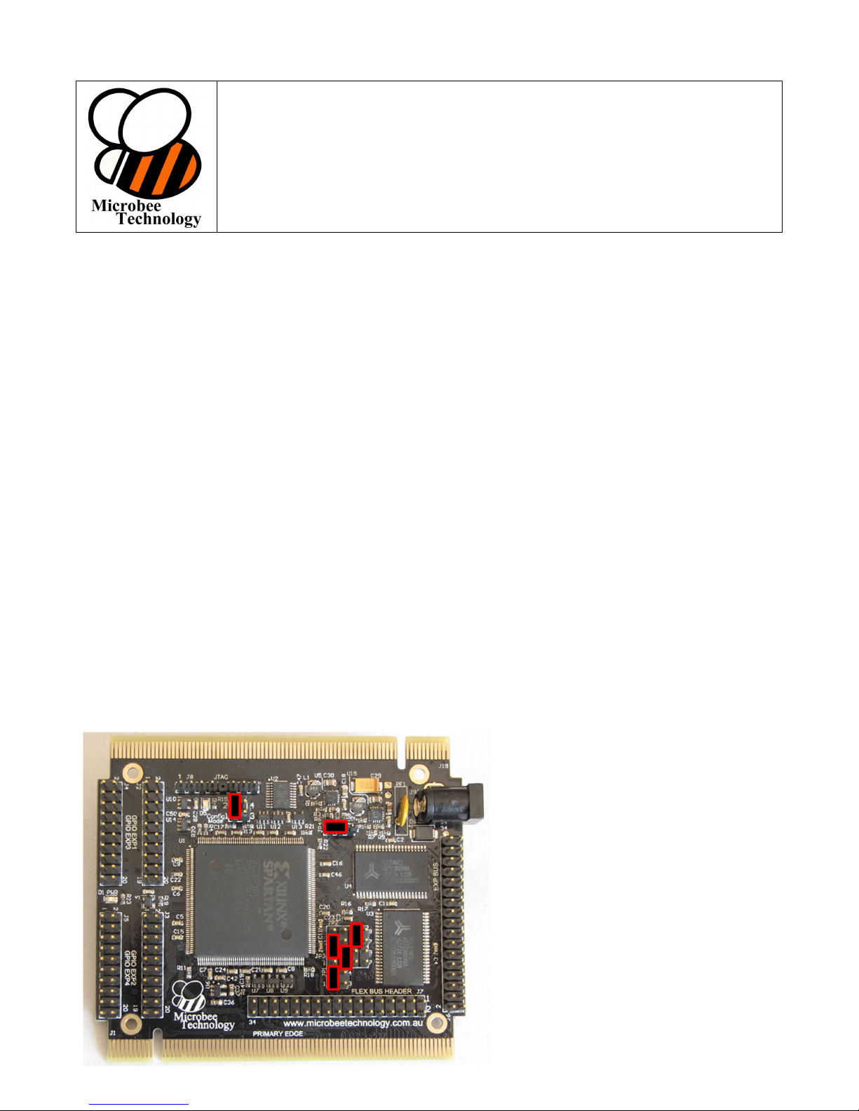
Configuring the FTM-3SE module Check that the jumpers on the FTM-3SE module are set as follows:
Jumper JP27 (Config Mode)
1-2 on, 3-4 off
(Slave parallel configuration)
Jumper JP4 (Power Enable)
1-2 on (closest to JP4 label)
N_PROG & DONE signal allocation:
JP2 – jumper pins 5 & 6
JP3 – jumper pins 3 & 4
LINK JP2 pin 1 to JP3 pin 2
FlexBus Chip select – select CS0
JP1 – jumper pins 1 & 2

Assemble the Tower System, ensuring that
the ‘Primary Side of each module is plugged
into the Primary elevator board.
The TWR-LCD-RGB elevator is the
‘Secondary’ side elevator in this stack.
[A] Insert the Power (Barrel type) connector
for the FTM-3SE module and turn on the
power. Note that the FTM-3SE does not
power up until power is detected from the
rest of the Tower system – this mode is set
by Jumper JP4. Please ensure that power
is applied via the Barrel connector prior to
powering the rest of the tower, otherwise
some bus contention may occur.
[B] Insert the Mini-USB cable into the
TWR-K70’s power / debug connector, but
leave the computer end of the cable out of
the computer for now (unpowered).
[C] Insert a Micro-SD card into the
TWR-K70 board with the FTM3SECI.BIN file
on it. This is the file that contains the Xilinx
Logic design that gets loaded into the FPGA.
Demonstration code
Requirements: CodeWarrior Eclipse Version 10.5.
If you have not already installed CodeWarrior, install this now, along with the drivers for the OSJTAG flash / debug
interface. Import the fb_xil_demo project into your workspace:

Connect the Tower System to the computer – the USB cable connected to the TWR-K70 is now connected ready for
programming the K70 Microcontroller. At this point the power lights on the Tower, the K70 & FTM-3SE modules
should light up, and the display backlight should also come on.
Press the debug button within CodeWarrior (the little green BUG symbol) and the project should compile and attempt
to program the K70 controller. If this is the first time downloading to the K70 within this session of CodeWarrior the
attempt will fail because of an error in the MK70FN1M0.mem memory definition file and you will get an error like this:
Select the MK70FN1M0.mem file within CodeWarrior and change the following line
From this:
…
reserved 0x20010000 0x5FFFFFFF
…
To this:
…
reserved 0x20010000 0x3FFFFFFF
…
and save the file.
Now you can press the debug button again & all should go well. You should see the status indicating that the K70 is
being programmed and the debugger will be ready to execute the code. Press the green ‘Play’ button to run the code.
Start the code running by
pressing the green ‘PLAY’
button.

At this point, the LCD screen should clear & you should see messages start appearing relating the progress of the
code through its routines. You should see black text on a light blue background as per the screen shot below.
If you watch carefully during the startup of the code, while the configuration file is being loaded from the SDcard, the
orange LED in one of the touch sensor pads on the TWR-K70 board shows SDcard activity. Also, at the end of
loading the configuration file into the Xilinx FPGA, the ‘DONE’ LED on the FTM-3SE will light, indicating that the
configuration has been successfully loaded into the FPGA. Now that the code is running if you were to attach LED’s to
the IO pins on the GPIO headers of the FTM-3SE board, you would see the LEDS going on and off in patterns as
related on the last line of the LCD display.
Demonstration complete.
While this demonstration is not very complex (testing on board SRAM and toggling I/O pins) it gives details of the
software & procedures required to load your own more complex FPGA designs into the FTM-3SE board & how to
interface to your logic via the FlexBus on the K70 processor.
Reference material:
The schematic of the Xilinx Logic for this demonstration has been included at the end of this Quick Start guide and
shows how to interface the K70 Flexbus in Multiplexed mode (8 bit data, latched address with ALE on CS1) and use
registers within the Xilinx logic design. The schematic was put together with Altium Designer (free trial available at
www.altium.com) , but can also be duplicated on the free Xilinx Webpack tools (see www.xilinx.com and search for
Webpack 14.7 download).

Here is the address map that is enabled within the sample Xilinx logic design:
Flexbus base address (0x60000000) + offset
Offset Read Access Write Access
0x0 SRAM 512K bank SRAM 512K bank
…
0x0007FFFF
0x0008XXX0 Pin Status GPIO-0 bits 0..7 Output register GPIO-0 bits 0..7
0x0008XXX1 Data direction GPIO-0 bits 0..7 Data direction GPIO-0 bits 0..7
0x0008XXX2 Pin Status GPIO-1 bits 0..7 Output register GPIO-1 bits 0..7
0x0008XXX3 Data direction GPIO-1 bits 0..7 Data direction GPIO-1 bits 0..7
0x0008XXX4 Pin Status GPIO-2 bits 0..7 Output register GPIO-2 bits 0..7
0x0008XXX5 Data direction GPIO-2 bits 0..7 Data direction GPIO-2 bits 0..7
0x0008XXX6 Pin Status GPIO-3 bits 0..7 Output register GPIO-3 bits 0..7
0x0008XXX7 Data direction GPIO-3 bits 0..7 Data direction GPIO-3 bits 0..7
0x0008XXX8 Pin Status GPIO-4 bits 0..7 Output register GPIO-4 bits 0..7
0x0008XXX9 Data direction GPIO-4 bits 0..7 Data direction GPIO-4 bits 0..7
0x0008XXXA Pin Status GPIO-5 bits 0..7 Output register GPIO-5 bits 0..7
0x0008XXXB Data direction GPIO-5 bits 0..7 Data direction GPIO-5 bits 0..7
0x0008XXXC Pin Status GPIO-6 bits 0..7 Output register GPIO-6 bits 0..7
0x0008XXXD Data direction GPIO-6 bits 0..7 Data direction GPIO-6 bits 0..7
0x0008XXXE Pin Status GPIO-7 bits 0..7 Output register GPIO-7 bits 0..7
0x0008XXXF Data direction GPIO-7 bits 0..7 Data direction GPIO-7 bits 0..7
These registers are mirrored through to offset 0x000BFFFF
The bits in the Data Direction registers when set (=1) specify the relevant GPIO bit as an OUTPUT.
0x000CXXXX SRAM bank select SRAM bank select
Bits 0 & 1 select which of 4 banks of 512K can be accessed at offset 0x0 by the Flexbus.
00 = Bank 0,
01 = Bank 1,
10 = Bank 2, and
11 = Bank 3.
This register is mirrored throughout the rest of the 1Mbyte address space from 0x000C0000 to
0x000FFFFF.
Freescale Semiconductor is a global leader in embedded processing solutions, providing industry leading products that are advancing the automotive,
consumer, industrial and networking markets. From microprocessors and microcontrollers to sensors, analog integrated circuits and connectivity – our
technologies are the foundation for the innovations that make our world greener, safer, healthier and more connected. For more information :
http://www.freescale.com/webapp/connect/displayPartnerProfile.sp partnerId=7180
© 2014 Microbee echnology Pty Ltd.
W: www.microbeetechnology.com.au E: info@microbeetechnology.com.au F: www.facebook.com/Microbee echnology
Table of contents
Popular Motherboard manuals by other brands


GigaDevice Semiconductor
GigaDevice Semiconductor GD32150R-EVAL user manual

MSI
MSI MAG B550 TOMAHAWK quick start

Microchip Technology
Microchip Technology Microsemi Silicon Sculptor 4 Quick start card

Aewin
Aewin MB-8303A user manual

Lutron Electronics
Lutron Electronics EcoSystem Energi Savr Node installation guide

Texas Instruments
Texas Instruments ALM2402FQ1EVM user guide