Microcyber NCS-MH105 User manual

NCS-MH105 Converter
User Manual
V1.5
Microcyber Inc.

I
Content
1Overview...................................................................................................................................1
2Performance Parameter.............................................................................................................2
3Structure and Working Principle...............................................................................................3
4Installation and Usage...............................................................................................................3
4.1 MODBUS Parameter Setting....................................................................................4
4.1.1 Brief Operation Steps for SDC625 Parameter Setting......................................5
4.1.2 NCS-MH105 Converter Parameters..................................................................5
4.2 Menu Tree.................................................................................................................8
4.3 Parameter Setting......................................................................................................9
4.3.1 Process Variables..............................................................................................9
4.3.2 Diag/Service......................................................................................................9
4.3.2.1 Test Device................................................................................................9
4.3.2.1.1 Status.........................................................................................9
4.3.2.1.2 Selftest.....................................................................................10
4.3.2.1.3 Device Reset............................................................................12
4.3.2.2 Calibration...............................................................................................14
4.3.2.2.1 Re-range..................................................................................14
4.3.2.2.1.1 Range Values...................................................................14
4.3.2.2.1.2 Apply Values...................................................................16
4.3.2.2.2 Analog Output.........................................................................18
4.3.2.2.2.1 Loop Current Mode.........................................................18
4.3.2.2.2.2 Loop Test.........................................................................20
4.3.2.2.2.3 D/A Trim.........................................................................22
4.3.2.2.3 Sensor Trim.............................................................................26
4.3.2.2.4 Coils Trim ...............................................................................28
4.3.2.2.5 Register Trim...........................................................................32
4.3.2.2.6 Recall Factory Trim ................................................................36
4.3.2.2.6.1 Restore to Default Factory ..............................................36
4.3.2.2.6.2 Save as Factory................................................................38
4.3.2.2.6.3 Restore to Factory ...........................................................39
4.3.3 Basic Setup......................................................................................................41
4.3.3.1 Tag ..........................................................................................................41
4.3.3.2 Long tag ..................................................................................................42
4.3.3.3 PV Unit....................................................................................................43
4.3.3.4 PV Damp.................................................................................................44
4.3.3.5 Range Values ..........................................................................................45
4.3.3.6 Device Information .................................................................................48

II
4.3.4 Detailed Setup.................................................................................................49
4.3.4.1 Device Variable Assignments.................................................................49
4.3.4.1.1 PV Is........................................................................................49
4.3.4.1.2 SV Is........................................................................................51
4.3.4.1.3 TV Is........................................................................................51
4.3.4.1.4 QV is .......................................................................................51
4.3.4.2 Sensors....................................................................................................51
4.3.4.2.1 Device Variable 0....................................................................52
4.3.4.2.1.1 Class................................................................................52
4.3.4.2.1.2 Unit..................................................................................53
4.3.4.2.1.3 USL.................................................................................54
4.3.4.2.1.4 LSL..................................................................................55
4.3.4.2.1.5 Min Span.........................................................................56
4.3.4.2.1.6 URV ................................................................................57
4.3.4.2.1.7 LRV.................................................................................58
4.3.4.2.2 Device Variable 1....................................................................60
4.3.4.2.3 Device Variable 2....................................................................60
4.3.4.2.4 Device Variable 3....................................................................60
4.3.4.2.5 Device Variable 4....................................................................60
4.3.4.2.6 Device Variable 5....................................................................60
4.3.4.3 Modbus....................................................................................................60
4.3.4.3.1 Modbus Variables ...................................................................60
4.3.4.3.1.1 Address............................................................................60
4.3.4.3.1.2 Baud Rate........................................................................61
4.3.4.3.1.3 Data Bits..........................................................................61
4.3.4.3.1.4 Parity ...............................................................................62
4.3.4.3.1.5 Stop Bits..........................................................................62
4.3.4.3.1.6 CRC Order.......................................................................63
4.3.4.3.1.7 Frame Idle Time..............................................................63
4.3.4.3.2 Device Status...........................................................................64
4.3.4.3.2.1 Device Status Register Address.......................................64
4.3.4.3.2.2 Device Status Bit Pattern.................................................65
4.3.4.3.3 PV RANGE.............................................................................65
4.3.4.3.3.1 PV Range Source.............................................................66
4.3.4.3.3.2 PV Range Option.............................................................66
4.3.4.3.3.3 Register Data Type..........................................................67
4.3.4.3.4 Device Variable 0....................................................................67
4.3.4.3.4.1 Default Unit.....................................................................68

III
4.3.4.3.4.2 MODBUS Function Code...............................................69
4.3.4.3.4.3 Register Address..............................................................69
4.3.4.3.4.4 Register Data Type..........................................................69
4.3.4.3.4.5 Scaling Factor..................................................................70
4.3.4.3.4.6 Upper Regsiter Address...................................................71
4.3.4.3.4.7 Lower Register Address..................................................72
4.3.4.3.5 Device Variable 1....................................................................72
4.3.4.3.6 Device Variable 2....................................................................72
4.3.4.3.7 Device Variable 3....................................................................72
4.3.4.3.8 Device Variable 4....................................................................72
4.3.4.3.9 Device Variable 5....................................................................72
4.3.4.4 Signal Condition......................................................................................73
4.3.4.4.1 PV LRV...................................................................................73
4.3.4.4.2 PV URV ..................................................................................74
4.3.4.4.3 PV Damp.................................................................................75
4.3.4.5 Output Condition.....................................................................................76
4.3.4.5.1 Analog Output.........................................................................76
4.3.4.5.1.1 Loop Current Mode.........................................................76
4.3.4.5.1.2 Loop Test.........................................................................77
4.3.4.5.1.3 D/A Trim.........................................................................79
4.3.4.5.2 HART Output..........................................................................83
4.3.4.5.2.1 Poll Address ....................................................................83
4.3.4.6 Operation Mode ......................................................................................85
4.3.4.7 Device Information .................................................................................85
4.3.5 Review ............................................................................................................86
5Fast Setting..............................................................................................................................91
6Device Diagnose and Maintenance.........................................................................................92
7Index 1 NCS-MH105 Converter Model Selection..................................................................93

1
1Overview
NCS-MH105 Converter is a new R&D converter between MODBUS-RTU protocol and HART
protocol. As MODBUS host, NCS-MH105 converter communicates with the device with
MODBUS-RTU communication function via RS485 interface, and it is able to convert the data in
the device to HART device variable output, supporting 4~20mA current output. NCS-MH105
converter is shown as Figure 1:
Figure 1 NCS-MH105 Converter
As a HART device, NCS-MH105 converter and PC can make up HART system via HART
modem. It is able to configure NCS-MH105 converter parameters via HART configuration
software, shown as Figure 2.
Figure 2 NCS-MH105 Converter System Connection
2
2Performance Parameter
NCS-MH105 Converter has powerful processing capacity, and the hardware parameters are shown
as following:
Parameter
Description
Bus Signal
4~20mA output with HART protocol digital communication
Bus Power
9~40V
Working Temperature
-40 ~85℃
Humidity Range
5% ~95%,non-dew
Mechanism Size
96mm ×56mm (can be customized)
CPU
M430F149
FLASH
60K
RAM
2K
EEPROM
2K
NCS-MH105 Converter and MODBUS device communicate via standard MODBUS-RTU
protocol. NCS-MH105 converter is used as master, and MODBUS device is used as slave. The
default communication parameters are shown as following:
Parameter
Default Value
Address
1
Baud Rate
9600
Data Bit
8
Stop Bit
1
CRC Calibration
low byte ahead
The MODBUS function codes supported by NCS-MH105 converter shown as following:
Function Code
Function
1
read loop status
2
read discrete input status
3
read keeping register value
4
read input register value
6
write loop
16
write multiple register values

3
3Structure and Working Principle
NCS-MH105 Converter supports 4 dynamic variables, 6 device variables. Via MODBUS register,
the data selected by MODBUS device is configured to NCS-MH105 Converter device variables,
and then it enters the mapping from device variable to dynamic variable, as the device output,
supporting 4~20mA analog signal output. NCS-MH105 Converter principle is shown as following
Figure 3:
MODBUS
REGISTER
MODBUS
Device
Configure Input Channel
Data Type
Register Addr
Unit
0
1
2
3
4
5
Device Variable
NCS-MH105 Converter
PV
SV
TV
QV
Dynamic Variable
Mapping from Device Variable to
Dynamic Variable
Control System
Process Varable
Analog
Channel
Process
Connection
Figure 3 NCS-MH105 Converter Principle
4Installation and Usage
The mechanism size of NCS-MH105 converter is 96 mm*56 mm, which not only matches
standard Adam module housing, also can be installed to device through positioning hole, shown as
Figure 4.

4
Figure 4 NCS-MH105 Converter Wiring Connection Terminal
The wiring connection of NCS-MH105 converter is shown as following:
Terminal
Signal Name
J1-4
HART+
J1-5
HART-
J2-4
GND
J2-5
B-
J2-6
A+
J2-7
5V
J2-8
GND
HART Bus gives power supply to NCS-MH105 converter. RS485 electrical interface requires an
external 5V power supply. It is recommended to use twisted-pair with shield, which improves
device anti-electromagnetic capacity. According to the wiring method above, the system is
powered on, firstly, the system will be self-testing, which will carry out system initialization,
protocol initialization, etc., and then starts to work.
4.1 MODBUS Parameter Setting
MODBUS communication parameter of NCS-MH105 converter is carried out via SDC625
configuration software, shown as Figure 5:

5
Figure 5 NCS-MH105 Converter Parameter Displayed in Configuration Software
4.1.1 Brief Operation Steps for SDC625 Parameter Setting
1) Click the parameters to set twice, and get the configure image.
2) Input the parameter value to set.
3) Click Set, the parameters will be yellow.
4) Click Send in the Tool bar to configure.
4.1.2 NCS-MH105 Converter Parameters
Name
Description
Operation Mode
Operation Method
0x00, "Configuration Mode"
0x01, "Normal Operation Mode"
Address
MODBUS Address
1~255
Baud Rate
Baud Rate
0x00, "1200"
0x01, "2400"
0x02, "4800"
0x03, "9600"
0x04, "19200"

6
0x05, "35700"
0x06, "38400"
0x07, "57600"
Data Bits
Data Bits
0x00, "7 Data Bits"
0x01, "8 Data Bits"
Parity
Parity
0x00, "NONE"
0x01, "ODD"
0x02, "EVEN"
Physical Standard
Physical Standard
0x00, "RS232"
0x01, "RS485"
0x02, "RS422"
Stop Bits
Stop Bits
0x00, "1 Stop Bits"
0x01, "2 Stop Bits"
CRC Order
CRC Order
0x00, "Low-High order"
0x01, "High-Low order"
Frame Idle Time
Frame Idle Time
0x00, "4 Character Times"
0x01, "5 Character Times"
0x02, "6 Character Times"
0x03, "7 Character Times"
0x04, "8 Character Times"
0x05, "9 Character Times"
0x06, "10 Character Times"
Device Status Register Address
Device Status Register
0~65535
Device Status Bit Pattern
Device Status Register Usage
0x0000, " NONE "
0x0001, "1 Bit"
0x0003, "2 Bit"
0x0007, "3 Bit"
0x000F, "4 Bit"
0x001F, "5 Bit"
0x003F, "6 Bit"
0x007F, "7 Bit"
0x00FF, "8 Bit"
0x01FF, "9 Bit"
0x03FF, "10 Bit"
0x07FF, "11 Bit"
0x0FFF, "12 Bit"
0x1FFF, "13 Bit"
0x3FFF, "14 Bit"
0x7FFF, "15 Bit"
0xFFFF, "16 Bit"
PV Range Source
PV Range Source
0x00, "Local"
0x01, "Remote"
PV Range Option
PV Range Option
0x00, "Read and Write"
0x01, "Read Only"
Default Unit
Device Variable Default Unit
MODBUS Function Code
MODBUS Function Code used by Device Variable
0x03, "READ HOLDING REGISTERS"
0x04, "READ INPUT REGISTERS"

7
Register Data Type
MODBUS Register Data Type
0x00, "Undefine"
0x01, "Char 0"
0x02, "Char 1"
0x03, "Unsigned Char 0"
0x04, "Unsigned Char 1"
0x05, "Short 0 1"
0x06, "Short 1 0"
0x07, "Unsigned Short 0 1"
0x08, "Unsigned Short 1 0"
0x09, "Long 0 1 2 3"
0x0A, "Long 1 0 3 2"
0x0B, "Long 3 2 1 0"
0x0C, "Long 2 3 0 1"
0x0D, "Unsigned Long 0 1 2 3"
0x0E, "Unsigned Long 1 0 3 2"
0x0F, "Unsigned Long 3 2 1 0"
0x10, "Unsigned Long 2 3 0 1"
0x11, "Float 0 1 2 3"
0x12, "Float 1 0 3 2"
0x13, "Float 3 2 1 0"
0x14, "Float 2 3 0 1"
Upper Register Address
Upper Register Address of Device Variable
0~65535
Lower Register Address
Lower Register Address of Device Variable
0~65535
Register Address
Register Address of Device Variable
0~65535
Scaling Factor
Scaling Factor of Device Variable
Floating number
8
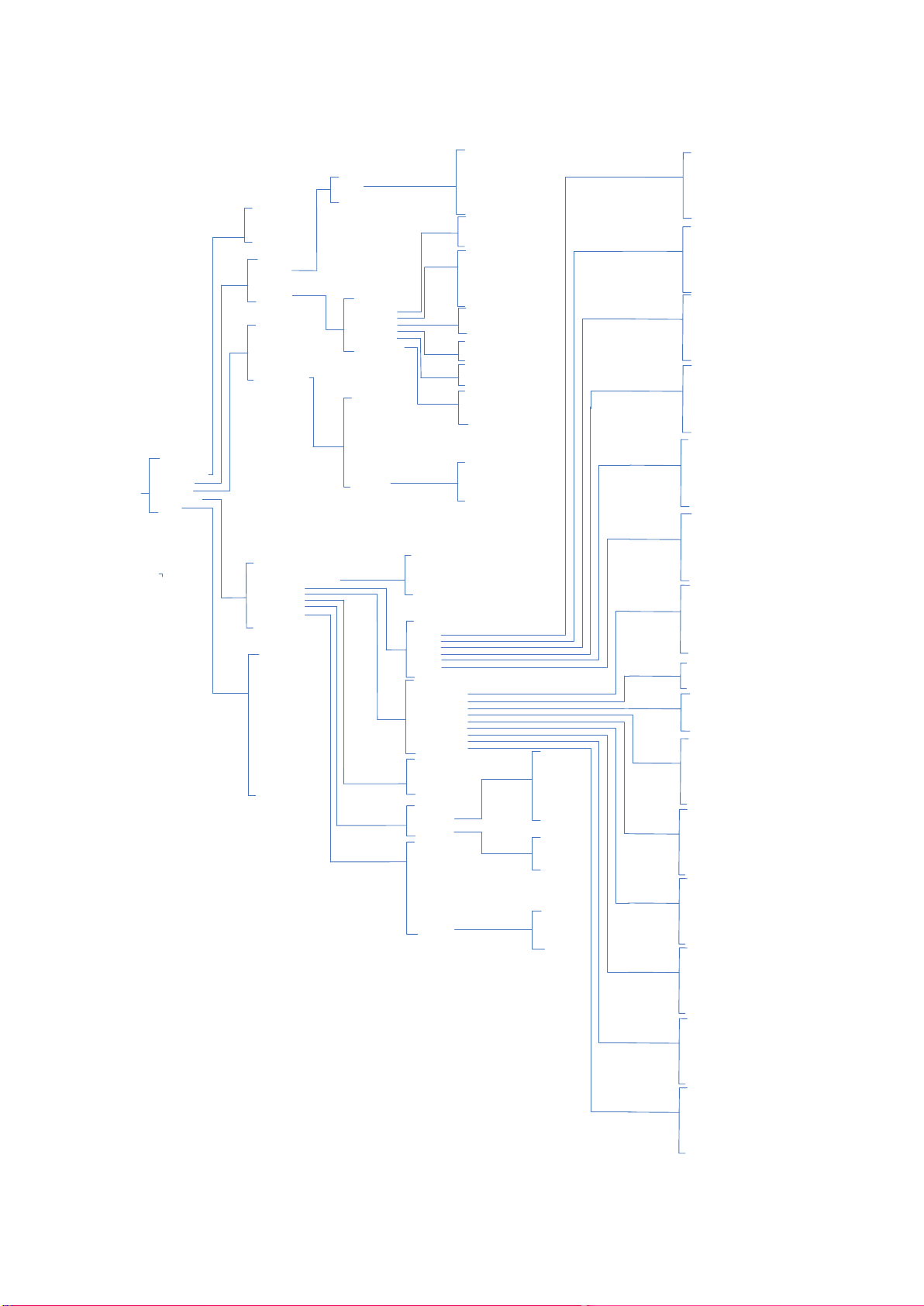
4.2 Menu Tree
1 Process Variables
2 Diag/Service
3 Basic Setup
4 Detailed Setup
5 Review
On line
1
Process Variables
1 PV
2 PV % rnge
3 PV LoopCurrent
4 Pv Range
1 Status
2 Test self
1 Test Device
2 Calibration
Diag/Service
2
Test Device
2-1 2-1-1
Calibration
1 Re-range
2 Anolog output
3 Sensor trim Sensor trim
2-4
2-4-1
Registers trim
2-4-4
1 Tag
2 Long Tag
3 Pv Unit
Basic Setup
3
Device information
5 Tag
6 Long Tag
7 Date
9 Descriptor
4 Cfg chng count
8 Write project
3-7
1 Device Variable Assignments
2 Sensors
3 MODBUS
4 Signal condition
Detailed Setup
Sensors
1 Device 0
4
4-1
1 MODBUS Variables
2 Device status
3 PV Range
Modbus
4-2
Signal Condition
2 PV URV
3 PV % rnge
4 PV Damp
1 PV LRV
4-3
1 Model
2 Manufaturer
3 Write project
4 Device id
Review
5
3 Device Test
1 Status group 0
2 Status group 1
3 Status group 2
4 Status group 3
5 Status group 4
6 Status group 5
7 Ext dev status
8 Operate mode 1
4 Coils trim
5 Registers trim
6 Recall factory trim
Re-range
1 Range Values
2 Apply Values
2-4-2 Anolog output
1 PV Loop current
2 PV Alrm typ
3 PV Channel flags
4 PV Xfer fnctn
5 Loop current mode
6 Loop test
7 D/A trim
2-4-3 1 Zero trim
1 Coils trim
Coils trim
2-4-5 1 Registers trim
2-4-6 Recall factory trim
2 Save as factory
1 Restore to default factory
3 Restore to factory
4 PV xfer fncnt
5 PV Damp
6 Range values
7 Device information
1 Manufacturer
2 Model
3 Dev id
10 Message
11 Final asmbly num
12 Revision #’s
Revision #’s
1 Universal rev
2 Fld dev rev
3 Software rev
3-7-12
5 Output condition
6 Device information
Device Variable Assignments
1 PV is
2 SV is
3 TV is
4 QV is
2 Device 1
3 Device 2
4 Device 3
5 Device 4
6 Device 5
7 Max dev vars
4 Device variable 0
5 Device variable 1
6 Device variable 2
7 Device variable 3
8 Device variable 4
9 Device variable 5
4-4
4-5 Output condition
1 Analog output
2 HART output
5 Tag
6 Long Tag
7 Date
9 Descriptor
4 Cfg chng count
8 Write project
1 Manufacturer
2 Model
3 Dev id
10 Message
11 Final asmbly num
12 Revision #’s
Revision #’s
1 Universal rev
2 Fld dev rev
3 Software rev
4-6
5 Cfg chng count
6 Max dev vars
7 Tag
8 Long tag
9 Descriptor
10 Message
11 Date
12 Final asmbly num
13 Universal rev
14 Fld dev rev
15 Software rev
16 Poll addr
17 Loop current mode
18 Num req preams
19 Num resp preams
Device 0
1 Classe
2 Unit
3 USL
4 LSL
5 Min span
6 URV
7 LRV
Device 1
1 Classe
2 Unit
3 USL
4 LSL
5 Min span
6 URV
7 LRV
Device 2
1 Classe
2 Unit
3 USL
4 LSL
5 Min span
6 URV
7 LRV
Device 3
1 Classe
2 Unit
3 USL
4 LSL
5 Min span
6 URV
7 LRV
Device 4
1 Classe
2 Unit
3 USL
4 LSL
5 Min span
6 URV
7 LRV
Device 5
1 Classe
2 Unit
3 USL
4 LSL
5 Min span
6 URV
7 LRV
MODBUS Variables
1 Address
2 Baud Rate
3 Data Bits
4 Parity
5 Stop Bits
6 CRC Order
7 Frame Idle Time
Device Status
1 Device Status register address
2 Device Status Bit parttren
PV Range
1 PV Range Source
2 PV Range Option
3 Register Data Type
Device variable 0
1 Default Unit
2 Modbus function Code
3 Register address
4 Register Date Type
5 Scaling Factor
6 Uper Register Address
7 Lower Register Address
Device variable 1
1 Default Unit
2 Modbus function Code
3 Register address
4 Register Date Type
5 Scaling Factor
6 Uper Register Address
7 Lower Register Address
Device variable 2
1 Default Unit
2 Modbus function Code
3 Register address
4 Register Date Type
5 Scaling Factor
6 Uper Register Address
7 Lower Register Address
Device variable 3
1 Default Unit
2 Modbus function Code
3 Register address
4 Register Date Type
5 Scaling Factor
6 Uper Register Address
7 Lower Register Address
Device variable 4
1 Default Unit
2 Modbus function Code
3 Register address
4 Register Date Type
5 Scaling Factor
6 Uper Register Address
7 Lower Register Address
Device variable 5
1 Default Unit
2 Modbus function Code
3 Register address
4 Register Date Type
5 Scaling Factor
6 Uper Register Address
7 Lower Register Address
1 PV Loop current
3 PV Channel flags
4 PV Xfer fnctn
Analog output
2 PV alrm typ
5 Loop current mode
6 Loop test
7 D/A trim
2 Num req preams
Hart output
1 Poll addr
3 Num resp preams
Status
Device information
4-2-1
4-2-2
4-2-3
4-2-4
4-2-5
4-2-6
4-3-1
4-3-2
4-3-3
4-3-4
4-3-5
4-3-6
4-3-7
4-3-8
4-3-9
4-5-1
4-5-2
4-6-12
7 Configuration Mode
Figure 6 Menu Tree
9
4.3 Parameter Setting
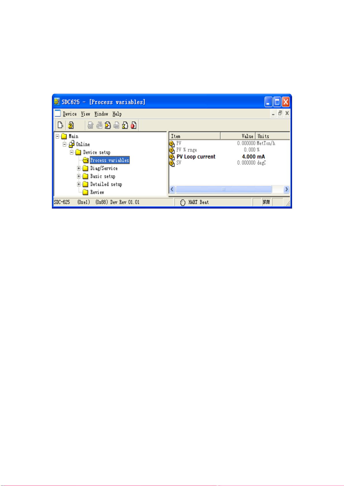
4.3.1 Process Variables
Process variable, is used to check PV and SV processing values.
Figure 7 Process Variables
4.3.2 Diag/Service
Diag/Service, provides device diagnose, service, etc.
4.3.2.1 Test Device
Test Device, can report device electric failure and other failures effected performance.
4.3.2.1.1 Status
Device additional status, and each bit represents each device status. It is needed to configure if the
user needs to use device status function, please refer to 4.3.4.3.2.

10
Figure 8 Device Diagnose Statue
4.3.2.1.2 Selftest
Device Selftest.
1) Click Selftest, to get Selftest interface, and click OK.
Figure 9 Selftest
2) Click ok, to test.

11
Figure 10 Confirm Selftest
3) Selftest is performing.
Figure 11 Performing Selftest
4) If there is no mistake, it will display “Self test OK”.
Figure 12 Selftest OK
5) Click OK, it will display return interface, and click OK to return.

12
Figure 13 Return Interface for Selftest OK
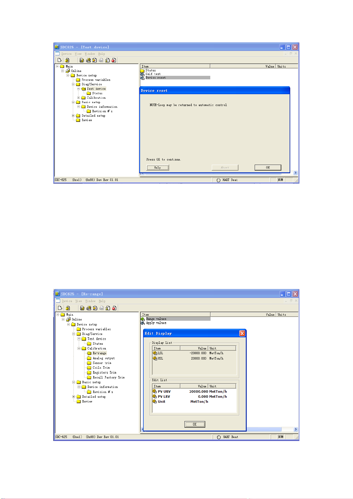
4.3.2.1.3 Device Reset
The steps for device reset as following:
1) Click Device reset twice and click OK.
Figure 14 Device Reset
2) To carry our device reset, click OK.

13
Figure 15 Confirm Device Reset
3) Device reset is performing, please wait.
Figure 16 Device Reset Performing
4) When device reset is successful, it will return and click OK.
Figure 17 Device Reset OK
5) Return and click OK.
14
Figure 18 Device Reset Return
4.3.2.2 Calibration
4.3.2.2.1 Re-range
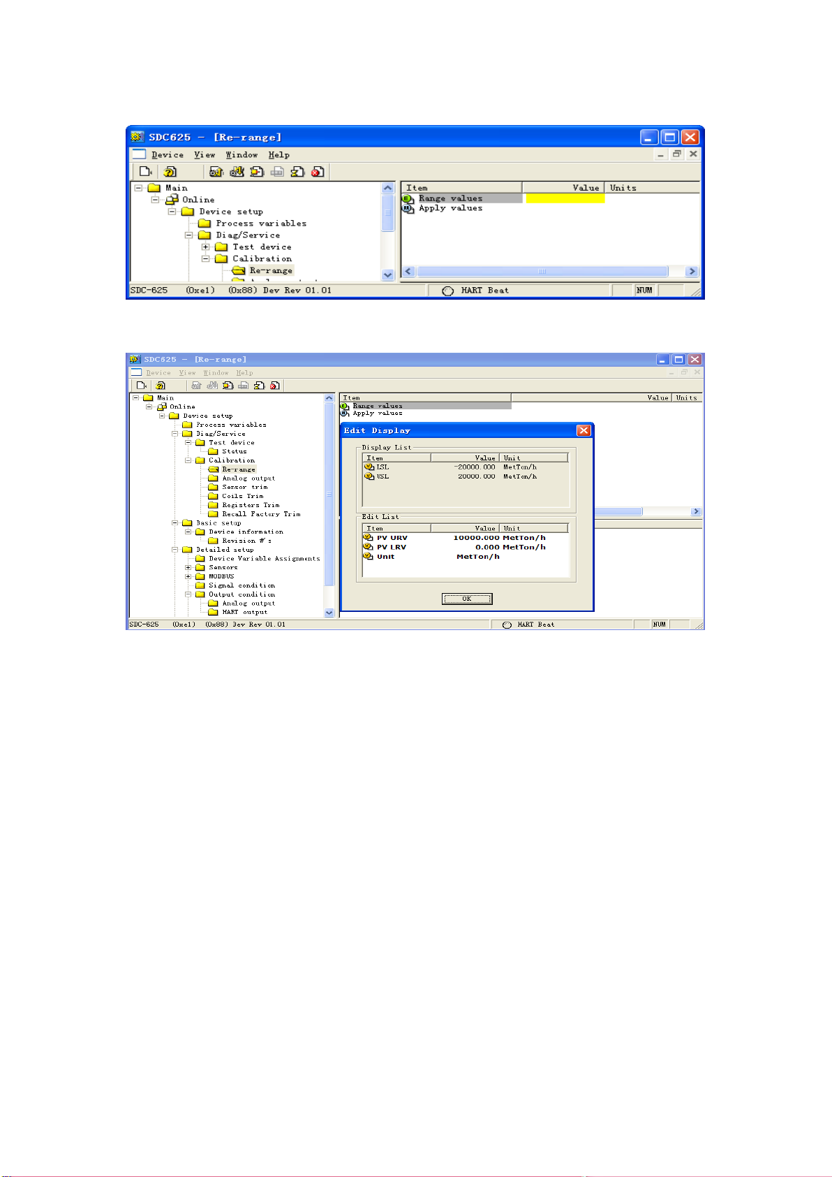
4.3.2.2.1.1 Range Values
PV range upper and lower value setting.
Example: Set PV URV from 20000 MetTon/h to 10000 MetTon/h.
1) Click Range values twice.
Figure 19 Range Value Setting

15
2) Click PV URV twice.
Figure 20 PV Range Setting
3) Click PV URV twice, input setting value 10000, and click OK.
Figure 21 Input PV Range Upper Limit Value
4) Click OK.
Figure 22 Confirm PV Range Upper Limit Setting
16
5) Click Send.
Figure 23 Send PV Range Upper Limit Value to Device
6) Click Range values twice, sending setting is successful.
Figure 24 PV Range Upper Limit Setting Successful
4.3.2.2.1.2 Apply Values
The method is used to set sensor present value to range upper and lower limit.
Example: To set present value as range lower limit.
1) Click Apply values twice and click OK.
Table of contents
Other Microcyber Media Converter manuals

Popular Media Converter manuals by other brands


 user guide")

Hengstler
Hengstler RI 36-H installation instructions

Soekris
Soekris dac1321 user manual

SEI
SEI ADVISOR AE100 Programming and installation guide

Baumer
Baumer HUBNER BERLIN AMG 11 FSL Mounting and operating instructions

Moxa Technologies
Moxa Technologies IMC-P101 Series Quick installation guide

IFM
IFM RM 3 Series operating instructions


