SECTION 2
PART REPLACEMENT AND ADJUSTMENT PROCEDURES
SECTION 3
SERVICING DIAGRAMS
1. STANDING PC BOARDS FOR SERVICING ..................... 3-1
2. CIRCUIT SYMBOLS AND
SUPPLEMENTARY EXPLANATION ..................................... 3-2
2-1. Precautions for Part Replacement .................................... 3-2
2-2. Solid Resistor Indication .................................................... 3-2
2-3. Capacitance Indication ....................................................... 3-2
2-4. Inductor Indication ............................................................. 3-3
2-5. Waveform and Voltage Measurement .............................. 3-3
3. PRINTED WIRING BOARD AND
SCHEMATIC DIAGRAM .......................................................... 3-5
4. BLOCK DIAGRAMS .................................................................. 3-7
4-1. Overall Block Diagram ...................................................... 3-7
4-2. Power Supply Block Diagram ........................................... 3-9
4-3. Front Display, Power Switch Block Diagram ................ 3-10
4-4. Main Block Diagrams .................................................... 3-13
4-5. Output Block Diagram .................................................. 3-17
5. CIRCUIT DIAGRAMS ........................................................... 3-19
5-1. Power Supply Circuit Diagram .................................... 3-19
5-2. Front Display, Power Switch Circuit Diagram ......... 3-21
5-3. Main Circuit Diagram ................................................... 3-24
5-4. Output Circuit Diagram ................................................ 3-29
5-5. Motor System Circuit Diagrams .................................. 3-34
6. PC BOARDS ............................................................................ 3-35
6-1. Power Supply PC Board ................................................ 3-35
6-2. Main PC Board ............................................................... 3-37
6-3. Output PC Board ............................................................ 3-47
CONTENTS
SECTION 1
GENERAL DESCRIPTIONS
1. PREPARATION FOR SERVICING ......................................... 1-1
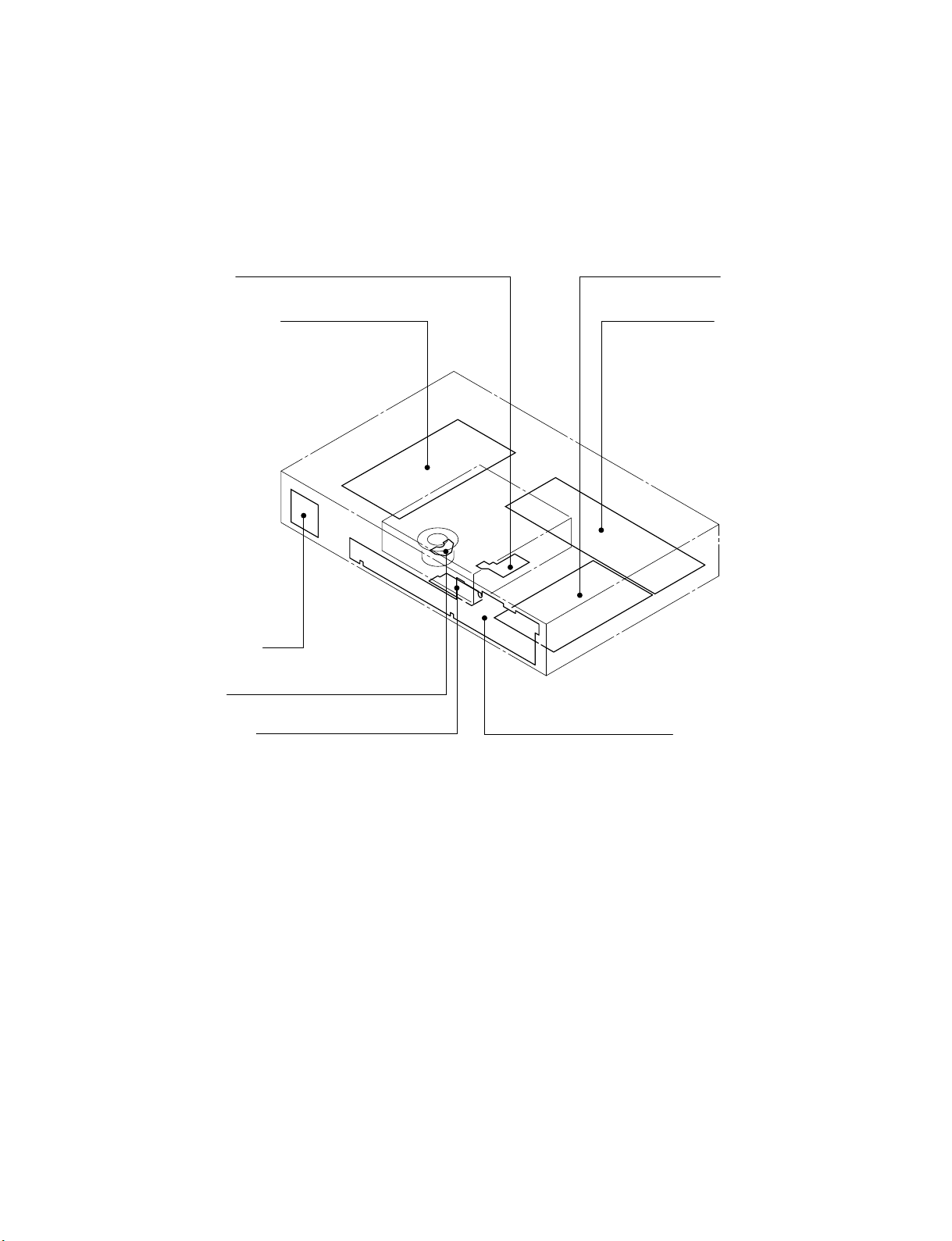
2. LOCATION OF MAIN PARTS AND
MECHANISM PARTS ............................................................... 1-2
2-1. Location of Main Parts ....................................................... 1-2
2-2. Location of Mechanism Parts ............................................ 1-3
1. REPLACEMENT OF MECHANICAL PARTS ................... 2-1
1-1. Cabinet Replacement ....................................................... 2-1
1-1-1. Top Cover ...................................................................... 2-1
1-1-2. Clamper Stay ................................................................ 2-1
1-1-3. Tray Panel ..................................................................... 2-2
1-1-4. Front Panel and Tray .................................................. 2-3
1-1-5. Rear Panel ..................................................................... 2-3
1-2. PC Board Replacement ................................................... 2-4
1-2-1. Main PC Board ............................................................. 2-4
1-2-2. Output PC Board ......................................................... 2-4
1-2-3. Power PC board ........................................................... 2-5
1-2-4. Front PC Board ............................................................ 2-5
1-3. Mechanism Parts ............................................................... 2-6
1-3-1. Mechanism Chassis Assembly ..................................... 2-6
1-3-2. Loading Belt .................................................................. 2-6
1-3-3. Loading Motor .............................................................. 2-7
1-3-4. Sub Chassis (with a pickup mechanism) ................... 2-7
1-3-5. Pickup Mechanism Assembly ...................................... 2-8
1-3-6. Gear A Assembly, Gear B and
Rack Gear Assembly ...................................................... 2-8
1-3-7. Feed Motor ...................................................................... 2-9
3. TROUBLESHOOTING ............................................................ 1-7
3-1. Main Circuit ....................................................................... 1 -7
3-1-1. Servo System ................................................................. 1-7
3-1-2. Location Diagram of Servo Test Point .................. 1-14
SECTION 4
PARTS LIST
SAFETY PRECAUTION ............................................................... 4-1
NOTICE ............................................................................................ 4-1
ABBREVIATIONS .......................................................................... 4-1
1. Integrated Circuit (IC) ........................................................ 4-1
2. Capacitor (Cap) .................................................................... 4-1
3. Resistor (Res) ......................................................................... 4-1
4. EXPLODED VIEWS ................................................................. 4-2
4-1. Packing Assembly ............................................................. 4-2
4-2. Chassis Assembly ............................................................... 4-3
4-3. Mechanism Assembly ........................................................ 4-4
5. PARTS LIST ............................................................................... 4-6