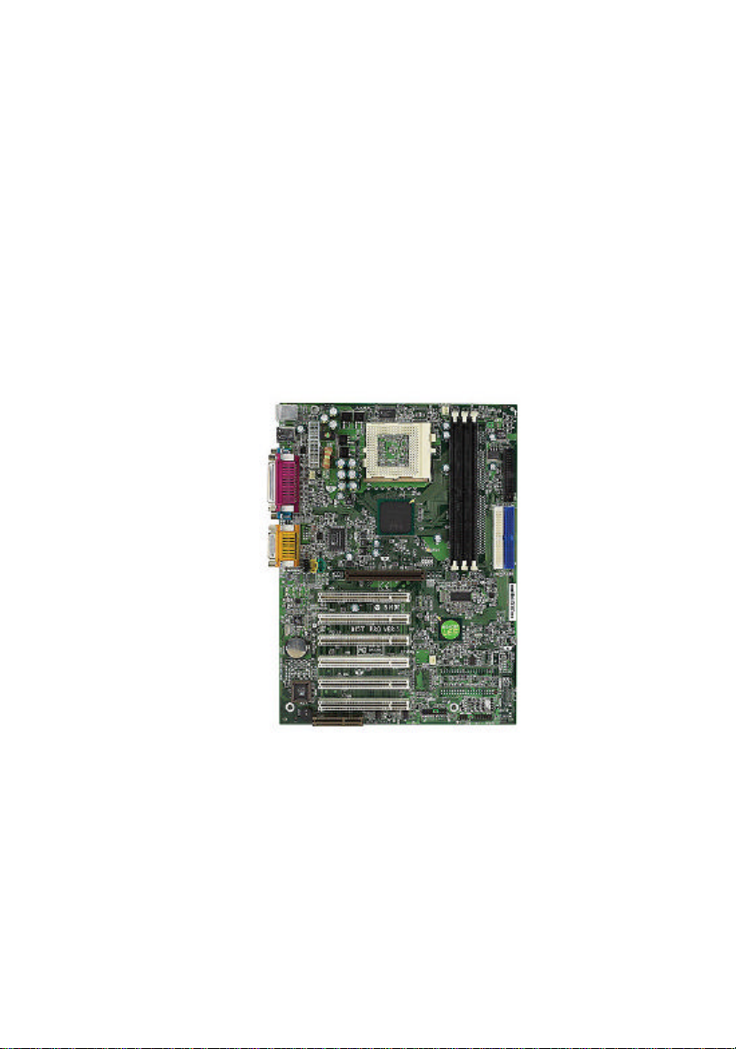
MSI MS-6337 User manual

i
MSI
MICRO-STAR INTERNATIONAL
MS-6337 LE5 ATX Mainboard
Version 5.0
G52-MA00370

ii
Manual Rev: 5.0
Release Date: May 2001
FCC-B Radio Frequency Interference Statement
This equipment has been tested and found to comply with the limits for a
class B digital device, pursuant to part 15 of the FCC rules. These limits are
designed to provide reasonable protection against harmful interference
when the equipment is operated in a commercial environment. This
equipment generates, uses and can radiate radio frequency energy and, if
not installed and used in accordance with the instruction manual, may cause
harmful interference to radio communications. Operation of this equipment in
a residential area is likely to cause harmful interference, in which case the
user will be required to correct the interference at his own expense.
Notice 1
The changes or modifications not expressly approved by the party
responsible for compliance could void the user's authority to operate the
equipment.
Notice 2
Shielded interface cables and A.C. power cord, if any, must be used in order
to comply with the emission limits.
VOIR LA NOTICE D'INSTALLATION AVANT DE RACCORDER AU
RESEAU.
Micro-Star International MS-6337 LE5
For Home or Office Use
Tested to comply
with FCC Standard

iii
Edition
May 2001
Copyright Notice
The material in this document is the intellectual property of
MICRO-STAR INTERNATIONAL. We take every care in the
preparation of this document, but no guarantee is given as to the
correctness of its contents. Our products are under continual
improvement and we reserve the right to make changes without
notice.
Trademarks
All trademarks used in this manual are the property of their
respective owners.
Intel and Pentium are registered trademarks of Intel Corporation.
PS/2 and OS/2 are registered trademarks of IBM Corporation.
Windows 95 and Windows NT are registered trademarks of Microsoft.
Netware is a registered trademark of Novell.
Award is a registered trademark of Award Software Inc.
Revision History
Revision Revision History Date
5.0 First release for 5.X PCB May 2001

iv
Safety Instructions
1. Always read the safety instructions carefully.
2. Keep this User’s Manual for future reference.
3. Keep this equipment away from humidity.
4. Lay this equipment on a reliable flat surface before setting it up.
5. The openings on the enclosure are for air convection hence protects the
equipment from overheating. DO NOT COVER THE OPENINGS.
6. Make sure the voltage of the power source and adjust properly
110/220V before connecting the equipment to the power inlet.
7. Place the power cord such a way that people cannot step on it. Do not
place anything over the power cord.
8. Always Unplug the Power Cord before inserting any add-on card or
module.
9. All cautions and warnings on the equipment should be noted.
10. Never pour any liquid into the opening that could damage or cause
electrical shock.
11. If any of the following situations arises, get the equipment checked by a
service personnel:
•The power cord or plug is damaged
•Liquid has penetrated into the equipment
•The equipment has been exposed to moisture
•The equipment has not work well or you cannot get it work
according to User’s Manual.
•The equipment has dropped and damaged
•If the equipment has obvious sign of breakage
12. DO NOT LEAVE THIS EQUIPMENT IN AN ENVIRONMENT
UNCONDITIONED, STORAGE TEMPERATURE ABOVE 600 C (1400F),
IT MAY DAMAGE THE EQUIPMENT.
CAUTION: Danger of explosion if battery is incorrectly replaced.
Replace only with the same or equivalent type recommended by the
manufacturer.

v

L
CONTENTS
Chapter 1. Introduction ............................................................... 1-1
Mainboard Specifications .......................................................... 1-2
Mainboard Layout ..................................................................... 1-4
Jumpers & Connectors .............................................................. 1-5
Back anel ............................................................................... 1-6
Chapter 2. AWARD® BIOS Setup ................................................. 2-1
Entering Setup .......................................................................... 2-2
Getting Help .............................................................................. 2-2
The Main Menu ......................................................................... 2-3
Standard CMOS Features ......................................................... 2-4
Advanced BIOS Features .......................................................... 2-5
Advanced Chipset Features ...................................................... 2-6
Integrated eripherals ............................................................... 2-7
ower Management Setup ........................................................2-8
N / CI Configurations ............................................................ 2-9
C Health Status .................................................................... 2-10
Frequency/Voltage Control ...................................................... 2-11
Load Fail-Safe/Optimized Defaults .......................................... 2-12
Set Supervisor/User assword ................................................ 2-13

Introduction
1-1
Chapter 1.
Introduction
The MS-6337 LE5 ATX mainboard is a high-performance computer
mainboard based on Inte ® 815EP chipset. The MS-6337 UMB (Universa
Motherboard) is optimized to support the who e series of new generation Inte ®
Pentium® III (FC-PGA/FC-PGA2) processors for high-end business/persona
desktop markets.
The Inte 815EP chipset contains two components: the 82815EP Memory
Contro er Hub (MCH) and the 82801BA I/O Contro er Hub 2 (ICH2). The
MCH integrates a 66/100/133-MHz, P6 fami y system bus contro er , AGP (2X/
4X) discrete graphics card, 100/133-MHz SDRAM contro er, and a high speed
acce erated hub architecture interface for communication with the ICH2. The
ICH2 integrates an U traATA/100 contro er, 2 USB host contro ers with a tota
of 4 ports, LPC interface contro er, FWH interface contro er, PCI interface
contro er, AC97 digita ink, integrated LAN contro er, and a hub interface for
communication with the MCH.
This chapter contains the fo owing topics:
Mainboard Specifications 1-2
Mainboard Layout 1-4
Jumpers & Connectors 1-5
Back Pane 1-6

Chapter 1
1-2
Mainboard Specifications
CPU
!Support Socket370 for the who e series of new generation Inte ® Pentium®
III(FC-PGA/FC-PGA2) processors.
!Support 500MHz, 550MHz, 600MHz, 633MHz, 667MHz, 700MHz, 733MHz,
800MHz, 866MHz, 933MHz, 1GHz, 1.1GHz, 1.13GHz and up to 1.2GHz.
Chipset
!Inte ® 815EP chipset
- 544 BGA
- AGP 4x/2x universa s ot
- Support 66/100/133MHz FSB
!Inte ® ICH2 chipset.
- AC97 Audio support
- 2 fu IDE channe s, up to ATA100
- Low pin count interface for SIO
- USB contro er 1.1
Main Memory
!Support three 168-pin DIMM sockets.
!Support a maximum memory size of 512MB SDRAM.
Slots
! One CNR (Communication Network Riser).
!One AGP (Acce erated Graphics Port) 2x/4x s ot
!Six PCI 2.2 32-bit Master PCI Bus s ots. A PCI s ots can be used as master.
!Support 3.3v/5v PCI bus Interface.
On-Board IDE
!An IDE contro er on the ICH2 chipset provides IDE HDD/CD-ROM with
PIO, Bus Master and U tra DMA 66/100 operation modes.
!Can connect up to two IDE devices.
On-Board Peripherals
!On-Board Periphera s inc ude:
- 1 f oppy port supports 2 FDD with 360K, 720K, 1.2M,
1.44M and 2.88Mbytes.
- 2 seria ports (COMA/COMB)

Introduction
1-3
- 1 para e port supports SPP/EPP/ECP mode
- 2 USB ports
Audio
! ICH2 chip integrated
! Support 2 channe audio
BIOS
!The mainboard BIOS provides P ug & P ay BIOS which detects the
periphera devices and expansion cards of the board automatica y.
!The mainboard provides a Desktop Management Interface (DMI) function
which records your mainboard specifications.
Dimension
!ATX Form Factor
Mounting
!6 mounting ho es.

Chapter 1
1-4
Mainboard Layout
MS-6337LE5ATXMainboard
BATT
+
ICH 2
Intel 815EP
chipset
J2
ATX
Power Supply
JFP1
CPUFAN
JBAT2
JMDM1
JWOL1
J7
FWH
PCI Slot 6
PCI Slot 5
PCI Slot 3
PCI Slot 2
PCI Slot 1
IDE 1
SYSFAN
DIMM 3
DIMM 1
DIMM 2
CNR
SW1
USB
Top : port 1
Bottom:
port 2
Top :
Parallel Port
Bottom:
COM A
COM B
Top : mouse
Bottom: keyboard
CD_IN
MODEM_IN
AUX_IN
Top :
Game
port
Bottom:
Line-Out
Line-In
Mic
SOCKET 370
FDD
AGP Slot

Introduction
1-5
Overclocking is operating a CPU/Processor beyond its
specified frequency. SW1 ju per is used for
overclocking.
The case connector block JFP1 allows you to connect
to the Power Switch, Reset Swtich, Speaker, Power
LED, and HDD LED on the case.
LED 5 indicates the DIMM power. When LED 5 is
powered on, do not atte pt to insert or re ove the
DIMM odule.
This connector allows you to connect to a LAN card
with Wake On LAN function. You can wake up the
co puter via re ote control through a local area
network.
JWOL1
This connector allows you to connect to a ode card
with Wake On Ring function. The connector will power
up the syste when a signal is received through the
ode card.
JMDM1
Jumpers & Connectors
SW1
!
"
#
$
JFP1
LED5
J2 is used to check the AGP chipset te perature on
AGP card. This function is reserved upon request.
J2
1
3
GND
MP_WAKEUP
5VSB
1
5
NC
GND
MDM_WAKEUP
NC
5VSB
J7 is a Front Panel Connector.
Speaker Output
Short 6-8 pin to activate AC97_SPKR
Short 8-10 pin to activate onboard Buzzer.
J7
PowerPower
PowerPower
Power
SwitchSwitch
SwitchSwitch
Switch
PowerPower
PowerPower
Power
LEDLED
LEDLED
LED
++
++
+
ResetReset
ResetReset
Reset
SwitchSwitch
SwitchSwitch
Switch
HDDHDD
HDDHDD
HDD
LEDLED
LEDLED
LED
++
++
+
SpeakerSpeaker
SpeakerSpeaker
Speaker
BuzzerBuzzer
BuzzerBuzzer
Buzzer
(short pin) 1414
1414
14 1515
1515
15
KeylockKeylock
KeylockKeylock
Keylock
DualDual
DualDual
Dual
ColorColor
ColorColor
Color
LEDLED
LEDLED
LED
SingleSingle
SingleSingle
Single
ColorColor
ColorColor
Color
LEDLED
LEDLED
LED
JBAT2 A battery ust be used to retain the ainboard
configuration in CMOS RAM. Short 1-2 pins of JBAT2
to store the CMOS data.
ReservedReserved
ReservedReserved
Reserved
IRTXIRTX
IRTXIRTX
IRTX
IRRXIRRX
IRRXIRRX
IRRX
ChassisChassis
ChassisChassis
Chassis
IntrusionIntrusion
IntrusionIntrusion
Intrusion
Buzzer/Buzzer/
Buzzer/Buzzer/
Buzzer/
SpeakerSpeaker
SpeakerSpeaker
Speaker
ReservedReserved
ReservedReserved
Reserved
GreenGreen
GreenGreen
Green
SwitchSwitch
SwitchSwitch
Switch
##
##
#
IRIR
IRIR
IR
Clear CMOS Keep CMOS
1
3
2
1
3
2

Chapter 1
1-6
Back Panel
USB Ports
USB Port 1
USB Port 2
1 2 3 4
PIN SIGNAL
1 VCC
2 -Data
3 +Data
4 GND
Line
Out
Line
In
Mouse Connector
Keyboard Connector
Joystick/MIDI
MIC
Audio Ports
COM A COM B
LPT 1
2
1
3
4
5
1
2
3
4
5
Pin1
Mouse DATA
Pin2
NC
Pin3
GND
Pin4
VCC
Pin5
Mouse Clock
Pin6
NC
Pin1
KBD DATA
Pin2
NC
Pin3
GND
Pin4
VCC
Pin5
KBD Clock
Pin6
NC

AWARD® BIOS Setup
2-1
Chapter 2. AWARD® BIOS Setup
The mainboard uses AWARD® BIOS ROM that provides a setup utility
for users to modify the basic system configuration The information is stored
in a battery-backed CMOS RAM so it retains the Setup information when the
power is turned off
This chapter provides you with the overview of the BIOS Setup program
It contains the following topics:
AWARD® BIOS Setup
Entering Setup 2-2
Getting Help 2-2
The Main Menu 2-3
Standard CMOS Features 2-4
Advanced BIOS Features 2-5
Advanced Chipset Features 2-6
Integrated Peripherals 2-7
Power Management Setup 2-8
PNP/PCI Configurations 2-9
PC Health Status 2-10
Frequency/Voltage Control 2-11
Load Fail-Safe/Optimized Defaults 2-12
Set Supervisor/User Password 2-13

Chapter 2
2-2
Entering Setup
Power on the computer When the below message appears briefly at
the bottom of the screen during the POST (Power On Self Test), press <Del>
key or simultaneously press <Ctrl>, <Alt>, and <Esc> keys to enter Setup
TO ENTER SETUP BEFORE BOOT, PRESS <CTRL-ALT-ESC>
OR <DEL> KEY
If the message disappears before you respond and you still wish to
enter Setup, restart the system by turning it OFF then On or pressing the
RESET button to try again You may also restart by simultaneously pressing
<Ctrl>, <Alt>, and <Delete> keys
Sub-Menu
If you find a right pointer symbol (as shown
in the right view) appears to the left of cer-
tain fields that means a sub-menu can be
launched from this field A sub-menu con-
tains additional options for a field parameter
You can use control keys ( ↑↓ ) to highlight
the field and press <Enter> to call up the sub-
menu Then you can use the control keys to
enter values and move from field to field
within a sub-menu If you want to return to
the main menu, just press the <Esc >
General Help <F1>
The BIOS setup program provides a General Help screen You can call up this
screen from any menu by simply pressing <F1> The Help screen lists the
appropriate keys to use and the possible selections for the highlighted item
Press <Esc> to exit the Help screen
After entering the Setup menu, the first menu you will see is the Main Menu
Main Menu
The main menu lists the setup functions you can make changes to You can
use the control keys ( ↑↓ ) to select the item The on-line description of the
highlighted setup function is displayed at the bottom of the screen
!IDE Primary Master
!IDE Primary Slave
!IDE Secondary Master
!IDE Secondary Slave
Getting Help

AWARD® BIOS Setup
2-3
The Main Menu
Once you enter Award® BIOS CMOS Setup Utility, the Main Menu (Figure 1)
will appear on the screen The Main Menu allows you to select from twelve
setup functions and two exit choices Use arrow keys to select among the
items and press <Enter> to accept or enter the sub-menu
Standard CMOS Features
Advanced BIOS Features
Advanced Chipset Features
Integrated Peripherals
Power Management Setup
PnP/PCI Configurations
PC Health Status
Frequency/Voltage Control
Load Fail-Safe Defaults
Load Optimized Defaults
Set Supervisor Password
Set User Password
Save & Exit Setup
Exit Without Saving
Esc : Quit F9: Menu in BIOS
F10 : Save & Exit Setup
Time, Date, Hard Disk Type...
↑ ↓ → ← : Select Item
CMOS Setup Utility - Copyright(C) 1984-2001 Award Software

Chapter 2
2-4
Standard CMOS Features
The items in Standard CMOS Features Menu are divided into 10 categories
Each category includes no, one or more than one setup items Use the arrow
keys to highlight the item and then use the <PgUp> or <PgDn> keys to select
the value you want in each item
↑ ↓ → ← Move Enter:Select +/-/PU/PD:Value F10:Save ESC:Exit F1:General Help
Date(mm:dd:yy): Fri, Feb 28,1999
Time(hh:mm:ss): 00:00:00
IDE Primary Master Press Enter 2557MB
IDE Primary Slave Press Enter None
IDE Secondary Master Press Enter None
IDE Secondary Slave Press Enter None
Drive A 1.44M, 3.5in.
Drive B None
Video EGA/VGA
Halt On All Errors
Base Memory 640K
Extended Memory 64512K
Total Memory 65536K
Item Help
Menu Level >
F5:Previous Values F6:Fail-Safe Defaults F7:Optimized Defaults
CMOS Setup Utility - Copyright(C) 1984-2001 Award Software
Sta dard CMOS Features

AWARD® BIOS Setup
2-5
Advanced BIOS Features
↑ ↓ → ← Move Enter:Select +/-/PU/PD:Value F10:Save ESC:Exit F1:General Help
Anti-Virus Protection Disabled
CPU Internal Cache Enabled
External Cache Enabled
CPU L2 Cache ECC Checking Enabled
Processor Number Feature Enabled
Quick Power On Self Test Enabled
First Boot Device Floppy
Second Boot Device HDD-0
Third Boot Device LS120
Fourth Boot Device Disabled
Swap Floppy Drive Disabled
Boot Up Floppy Seek Enabled
Boot Up NumLock Status On
Gate A20 Option Fast
Typematic Rate Setting Disabled
Typematic Rate (Chars/Sec) 6
Typematic Delay (Msec) 250
Security Option Setup
OS Select for DRAM > 64MB Non-OS2
HDD S.M.A.R.T. Capability Disabled
Report No FDD For WIN 95 No
Full Screen LOGO Show Enabled
Item Help
Menu Level >
F5:Previous Values F6:Fail-Safe Defaults F7:Optimized Defaults
CMOS Setup Utility - Copyright(C) 1984-2001 Award Software
Adva ced BIOS Features

Chapter 2
2-6
The Advanced Chipset Features Setup option is used to change the values of
the chipset registers These registers control most of the system options in the
computer
Choose the ADVANCED CHIPSET FEATURES from the Main Menu
and the following screen will appear
Advanced Chipset Features
↑ ↓ → ← Move Enter:Select +/-/PU/PD:Value F10:Save ESC:Exit F1:General Help
Note: Change these settings only if you are familiar with the chipset.
SDRAM CAS Latency Time Auto
SDRAM Cycle Time Tras/Trc 7/9
SDRAM RAS-to-CAS Delay 3
SDRAM RAS Precharge Time 3
System BIOS Cacheable Disabled
Video BIOS Cacheable Disabled
Memory Hole at 15M-16M Disabled
CPU Latency Timer Enabled
Delayed Transaction Enabled
AGP Graphics Aperture Size 64MB
System Memory Frequency Auto
Item Help
Menu Level >
F5:Previous Values F6:Fail-Safe Defaults F7:Optimized Defaults
CMOS Setup Utility - Copyright(C) 1984-2001 Award Software
Adva ced Chipset Features

AWARD® BIOS Setup
2-7
Integrated Peripherals
CMOS Setup Utility - Copyright(C) 1984-2001 Award Software
I tegrated Peripherals
On-Chip Primary PCI IDE Enabled
On-Chip Secondary PCI IDE Enabled
IDE Primary Master PIO Auto
IDE Primary Slave PIO Auto
IDE Secondary Master PIO Auto
IDE Secondary Slave PIO Auto
IDE Primary Master UDMA Auto
IDE Primary Slave UDMA Auto
IDE Secondary Master UDMA Auto
IDE Secondary Slave UDMA Auto
USB Controller Enabled
USB Keyboard Support Disabled
USB Mouse Support Disabled
Init Display First PCI Slot
AC97 Audio Auto
AC97 Modem Auto
Gate A20 Enabled
IDE HDD Block Mode Enabled
Keyboard Power On Disabled
POWER ON Function Button Only
KB Power On Password Enter
Hot Key Power ON Ctrl-F1
Onboard FDC Controller Enabled
Onboard Serial Port 1 3F8/IRQ4
Onboard Serial Port 2 2F8/IRQ3
UART Mode Select Normal
RxD, TxD Active Hi, Lo
IR Transmition Delay Enabled
UR2 Duplex Mode Half
USE IR Pins IR-Rx2Tx2
Onboard Parallel Port 378/IRQ7
Parallel Port Mode SPP
EPP Mode Select EPP 1.7
ECP Mode Use UDMA 3
PWRON After PWR-Fail Off
Game Port Address 201
Midi Port Address 290
Midi Port IRQ 10
Power Status LED Single
Item Help
Menu Level >
↑ ↓ → ← Move Enter:Select +/-/PU/PD:Value F10:Save ESC:Exit F1:General Help
F5:Previous Values F6:Fail-Safe Defaults F7:Optimized Defaults

Chapter 2
2-8
Power Manage ent Setup
The Power Management Setup allows you to configure you system to most
effectively save energy while operating in a manner consistent with your own
style of computer use
IPCA Function Enabled
ACPI Suspend Type S1(POS)
Power Management User Define
Video Off Method DPMS
Video Off In Suspend Yes
Suspend Type Stop Grant
Modem Use IRQ 3
Suspend Mode Disabled
HDD Power Down Disabled
Soft-Off by PWR-BTTN Instant-Off
Wake-Up by PCI Card Disabled
Power On by Ring Enabled
Wake-Up On LAN Enabled
USB KB Wake-Up From S3 Disabled
CPU Thermal-Throttling 50.0%
Resume By Alarm Disabled
Date(of Month) Alarm 0
Date(hh:mm:ss) Alarm 0 0 0
**Reload Global Timer Events**
Primary IDE 0 Disabled
Primary IDE 1 Disabled
Secondary IDE 0 Disabled
Secondary IDE 1 Disabled
FDD, COM, LPT Port Disabled
PCI PIRQ[A-D]# Disabled
Item Help
Menu Level >
↑ ↓ → ← Move Enter:Select +/-/PU/PD:Value F10:Save ESC:Exit F1:General Help
F5:Previous Values F6:Fail-Safe Defaults F7:Optimized Defaults
CMOS Setup Utility - Copyright(C) 1984-2001 Award Software
Power Ma ageme t Setup
Table of contents
Other MSI Motherboard manuals

MSI
MSI A320M PRO-M2 User manual

MSI
MSI MS-7036 User manual

MSI
MSI Z87-G43 GAMING User manual

MSI
MSI MEG Z590 UNIFY User manual

MSI
MSI X58 PRO MS-7522 User manual

MSI
MSI P31 NEO-F - Motherboard - ATX User manual

MSI
MSI MS-6380 User manual

MSI
MSI Microstar MS5116 User manual

MSI
MSI H310M PRO-VDH PLUS User manual

MSI
MSI B350M MORTAR User manual
Popular Motherboard manuals by other brands

Fujitsu Siemens Computers
Fujitsu Siemens Computers D1215 Technical manual

Congatec
Congatec SMARC 2.0 conga-SEVAL user guide

Texas Instruments
Texas Instruments ADC1 D (RF )RB Series user guide

Analog Devices
Analog Devices EVAL-AD5161DBZ user guide

Foxconn
Foxconn H61MXL Series user manual

Asus
Asus P8Q77-M manual