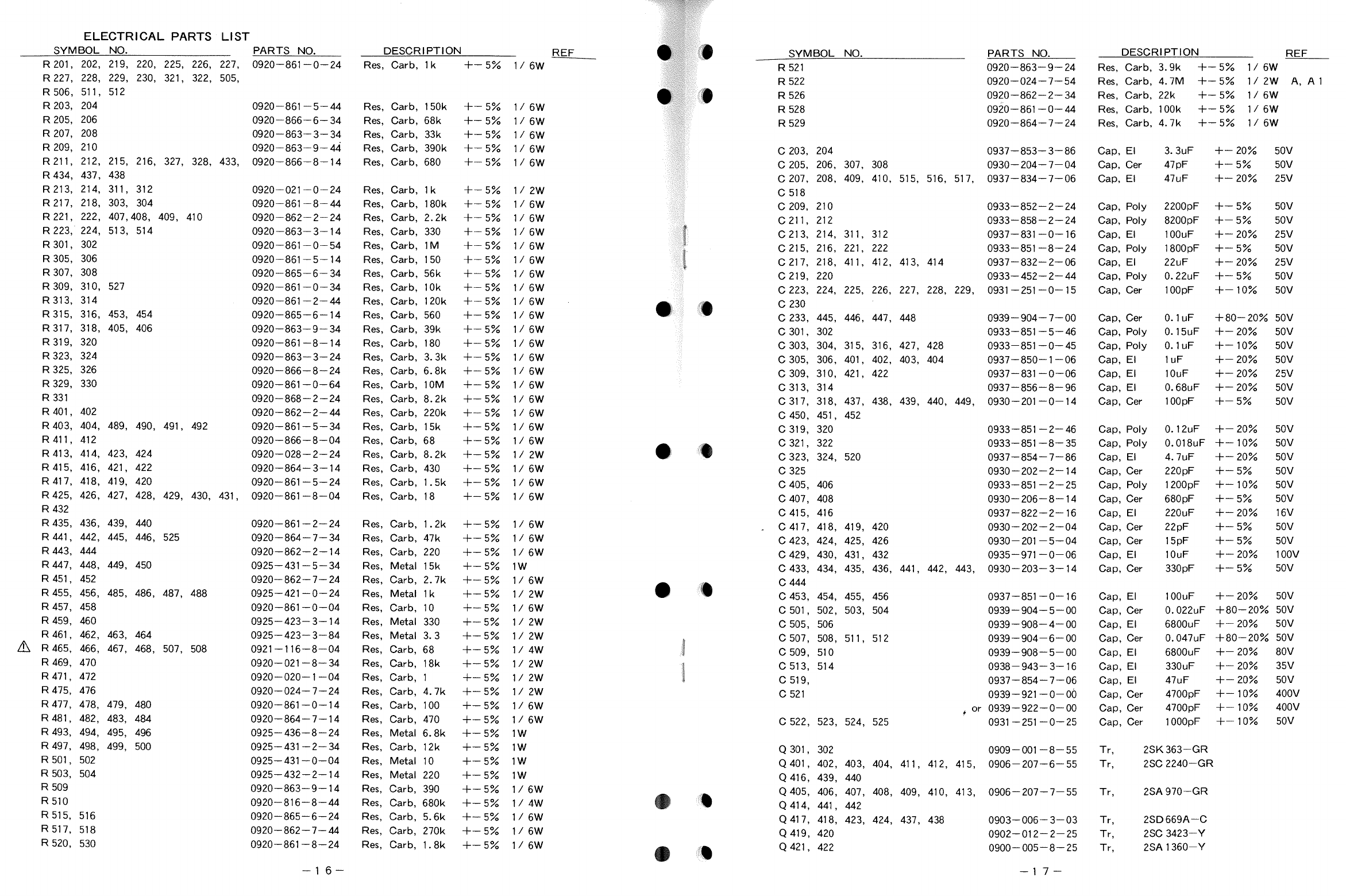
manuals.online logo
Brands
  1. Home
  2. •
  3. Brands
  4. •
  5. NAD
  6. •
  7. Amplifier
  8. •
  9. NAD 3240 User manual

NAD 3240 User manual

: NAD
SERVICE
_
MANUAL
m
Z
1958BYNAD
555
PAINTEDINJAPAN
STARTING SERIAL
NUMBER
A
340
IJ00001
3240
NAD
ELECTRONICS
INTEGRATED
AMPLIFIER
Ii
II
PAGE
CONTENTS
3
REAR/FRONT
PANEL
LAYOUT
4
SPECIFICATIONS
5
ALIGNMENT
METHOD
6
PREAMP,
VOLUME
PCB
LAYOUT
7—8
AMPLIFIER
PCB
LAYOUT
9—10
AMPLIFIER
SCHEMATIC
11—12
WIRING
DIAGRAM
13
TRANSFORMER
WIRING
(MULTI—VOLTAGE)
14
PREAMP,
VOLUME
PCB
PARTS
LOCATION
15
AMPLIFIER
PCB
PARTS
LOCATION
16—19
ELECTRICAL
PARTS LIST
20—21
EXPLODED
VIEW
22—24
EXPLODED
PARTS
LIST
25
PACKING
DIAGRAM
SERVICE
SAFETY
PRECAUTIONS
(UL)
1.
Use
exact
replacement
parts
for
critical
locations,
marked
“
2.
Return
lead
dress
to
original
position,
and
re—install
protective
covers.
3.
Before
returning
to customer,
test
for
shock
hazard;
use
either
method
A
or
B:
A.
Leakage
test,
“cold”:
1.
Unplug
AC
cord;
turn
power
switch
ON.
Power
Amplifier
Section
CONTINUOUS
AVERAGE
POWER
OUTPUT
AT
8
OHMS (minimum RMS
40W
(16dBW)
power
per
channel,
both channels
driven,
with
no
more
than
the
rated distortion)
Rated distortion
(THD)
20Hz—
20kHz
0.03%
Clipping power,
1kHz
(maximum
50W
continuous
power
per
channel)
Dynamic Headroom
at
8
ohms
Dynamic power
(maximum)
8
ohms
short—term
power
per
channel)
4
ohms
2
ohms
Damping
factor
Slew
factor
Slew
rate
T.H.D.
and
SMPTE.I.M.
distortion
from
250
mW
to
rated
output
Input
Impedance
Input
sensitivity
for
1
Watt!
40
Watts
out
Power
amp
gain
Preamplifier
Section
Phono
Input
Input
Impedance
Input
Sensitivity
(1kHz)
Signal—to—Noise
Ratio
with
cartritdge
connected,
A—weighted
Input
Overload
at
20
Hz! lkHz/2OkHz
RIAA
Accuracy
High—Level
Inputs
(CD.
Video,
Tape)
Input
Impedance
Input
Sensitivity
Signal
—to—Noise
ratio,A—weighted
Input
Overload
Frequency
Responce
Outputs
Preamp
output
impedance
Tape
output
impedance
Physical
Specifications
Width
x
Height
x
Depth
Net
Weight
Shipping
Weight
Power
Consumption
42
x
10.8
x
38 cm
16.5
x
42.5
x 15 in
6.7kg
(14
lbs
14
oz)
8kg (17
lb
12
oz)
50/
60Hz
at
110, 120,
220,
or
240
VAC
200W
8.
CO
Input
9.
Video input
10.
lap.
input/Output.
11.
Preanrp
Out.
Main
in.
12.
Sort
Clipping.
13.
Speaker
inrpedance.
REAR PANEL
I.
AC
Line
Cord.
2. AC
Convenience
Outlets
3.
Speakers
A.
4.
SpeakerS
8.
5.
Phono
Ground
6.
Ptruno
lrrprar
7.
Tuner
Input.
65
LE
PANNEAU
ARRIERE
1.
Cordon
dalimentatiun
2.
Poses
CA
3.
Enceintes
A
4.
Enceintes
8
5.
Masse
phonoicuteur
6.
Entrée
phony
7.
Entrée
toner
8.
Eetree
iecteur de
disque
compact
9.
Entree
video
10.
Entree/Sortie
magnetophone
11.
Sortie
de prdamplilication
12.
Ecrdiage
en
douceur
13.
Impedance
RUCKSEITE
1.
Netzkabel
2.
Sekundar.Stevkdosen
3.
Anschlusse
tur
Lautsprechergruppe A
4.
AnsehIusse
tur
Lautsprechergruppe 8
5.
Masseanschlufl
ut
Plattenspieler
6.
Plattenspieier-Eingang
7.
Tuner-Eingang
8.
CDEingang
9.
Video
10.
Tonbandgerat
Eingang
Ausgang
11.
VoruerslarkerAusgang
Endverstarker.Erngang
12.
lmpulsbegrenzungs.Schalter
13.
Lautsprecherirnpndanz.Sctralter
89W
113
4132
Specifications
NAD
3240PE
Stereo
Amplifier
Controls
Treble
±7dB
at
10kHz
Bass
±10dB
at
50Hz
Measured
in
accordance
with
EIA
Standerd
RS—
490
(formerly
HF Bass
Equalization
+3dB
at
70Hz
A—
202)
.
±6dB
at
40Hz
Measurements
referred
to
8
ohms
are
taken
with
Speaker
Impedance Infrasonic
Filter
—3dB
at
12Hz
selector
at”
8
ohm
(High)
.“
Measurements
for
4
and
2
ohms
are
12dB/octave
taken
with
impedance
selector
at”
4
ohm
(Normal)
“
Low Level
(audio
muting)
—20dB
Specifications are
those
in
effect
at
tIre
tone
oiprioting.
specifications
or
designs
at any
hive
without
notice.
+
A
—
—
L
+
iuecousc
swincneo
w
non
Rwsoint
On/OW
MAX
c•:’
•)
*
I!E
0
!_ui
1
,
I
NAD
ELECTRONICS,
INC
rosen
CD
unen
oar
tM
POE
OuT
401515
OOS000/L000CiN
B(t*a
L....nuer,..J
us
or,
TION:
En
Lcs
coriscoucsccs
CAUTION TO
REDUCE
GuuvcS
Ovi
POURARiENT
ThE
RISK OF
cLEcnRlc
cN
ocsvnnco
Sc
TcNTcz
5100CR.
DO
NOT
REMOVc
PROD
OUVRIR
LOPPARcIL
concn
OR
SACKI
cn
Dr
nOvCnER
ovo
NO
USERSEROICEA8LE
cnr,rPOsuNTS
INncRNcs
mATS
INSIDE.
REFER
12
sons
Lu
Pncscscc
5
Usc
scrrviosa
To
QIJAUFIED
pcRsosNE
ovvLlFlcc
ScRniCE
PERSONNEL
FRONT PANEL
LE
PANNEAU
AVANT
FRONTSEITE
1.
Power
9.
Menu
1.
Alrmentation
8.
Mono
1.
Nelanchalter
8.
Mono
SterenScflalter
2.
Phones
9.
Tape Monitot
2.
Casque
decovte
9.
Commutateur
de
suroeillance
de
bande
2.
KopthorerAnscnivU
9. Vor
USer
BandSchalter
3.
Speaker
Selentoe
10.
Input
Selector
3.
SAlectevr
deeceintes
10.
Selecteur
U
entree
3.
Lautspreoher-Wairlschalier
I
0.
Engangs.Wahischalter
4.
Bass
11.
Low
Level
4.
Graves
11.
Low
level..
4.
Ratsteller
ft.
Sctralter
tur
Laurstarkeabsnnkung
5.
Treble
12.
LoudneSs
5.
Argus
12.
Commorarevr de contovr
sonore
5.
Hohensteller
12.
Gennrrictrtige/Lautstarke.Einstellung
6.
Bass
EO, 13.
Volv,ne/Balance
6.
Bass
Eq
13.
SVlvrrte/Eifvilibrage
6. BaD
EqvalizerSchalter
13.
LavtstarkeiBalance.Stellnr
7.
intrasneic
Filter
Ott
7.
Filtre
intrasnnigve
7.
Schalter
yr
inlrauchallFilter
1
N.AD
Soanu
Aree#rtr.e
PENNER
ENVELOPE
noons
suer
CLiPnrso
NAG
reserves
tile
right
to
change
±6dB
160W
200W
250W
>
50
>
50
1
5V/Jsec
<0.03%
22kohm
l6OmV/
1.OV
25dB
(
18X)
R°
47kohm,
C=
100pF
0. 55mV for
1
Watt out
3.
5mV
for
40
Watts
out
76dB
re
5mV
20/
180/
l500mV
±0.5dB
R
l5kohm,
C=
lOOpF
26mV for
1W
out
160mV for
40W
out
86dB
re
1W
out
102dB
re
40W
out
>
1OV
20Hz—
20kHz
±0.5dB
6000hm
Source
Z+l0000hm
2
3
5
67u
9
11
12
13
10
—3—
—4—
ALIGNMENT
METHOD
MAIN
AMPLIFIER
ALIGNMENT
IMPORTANT
NOTES:
1)
Before
adjusting,
remove
input
signal
and
load,
and
set Speaker
Impedance
switch
to
8
ohms.
(Reset
to
4
ohms
when
finished.)
2)
These
adjustments
are
always
necessary
after
repair
to main
amplifier.
3)
After
repair,
it
is
recommended
to
use
current
limiter
(40-80W
lightbulb)
in
series
with
AC
mains
line,
for
initial
turn-on.
A.
CENTER
VOLTAGE
ADJUSTMENT
1.
Connect
DVM
across
L
channel
(R
channel)
output
terminals.
2.
Turn
on,
and
adjust
VR-401
(VR-402)
for
reading
of
0V ±
30
mVDC.
B.
IDLE
CURRENT
ADJUSTMENT
1.
Remove
solder
short
across
R-471
and
R-472.
2.
Connect
DVM
across
R-471.
3.
Turn
on
and
adjust
VR-403
for
reading
of
28
mV
±
2
mVDC.
4.
Repeat,
using
R-472,
adjust
VR-404.
C.
FINAL
ADJUSTMENT
.
.
1.
Leave
power
on
minimum
5
minutes.
2.
Repeat
center
voltage
and
idle
current
adjustments.
3.
When finished,
replace
solder
short
across
R-471
and
R-472.
t’1
I
(J+
(S
4
.
C
2
LL
.1
213
I
Iv
T
0
(SIS
a:
1
a:
m
C26
1IC201
(1
P2
C226
11
IF—
+
P205
‘tho’s
I
..J
L
C223
C201
°‘
2Oi
I+It
1
.
P207
—Wv—-—
P2’),
-.
-
HF
c2;
C
233
AMPLIFIER
ALIGNMENT
POINT
PREAMP,
VOLUME
PCB
LAYOUT
U
u
(7)
—
c
c
L1
LZI
P217
—wv—
—
(‘4 (‘4
(‘4
0j
0±
TT
.
—5—
AMPLIFIER
PCB
LAYOUT
0423 0429
D411@
_______
I
R471
+
C421
L±
P461
R45
o,I
--
-
,Ii
‘‘
<‘‘
C423
—w.—-
oTn
cTo
_*_
0419
R459+
Ii
I
C302
T7\
P457
____
HF
‘ü)
__
__
-,f--,
H1
304
R447
0415 0435
VP403
0421
[_J
—w———
p449
_____
C417
c
LO
VR401
—.-——-
C425
R455
R303
C304
0411
P439
—IF
______
C305
—
041
3
tFji(Jl
409Q
415
P310
P304
——-—
C419
R307
P411
HF
0406
R306
D407
1V)
0402
P425
P429
P308
Q409”’
—--—
—w.—
R475
J)
P1.37
P467
01
0405
I
gj_
Lc
C429
R443
C455
SW7
T
T
+
C431
—tf
R309
T
P318
C310
LO R403
I
jLni
P515
—
W
C405
P320
C316
Icti
_ti1
11
Tc)I
LX
—II—
HF
-v
R319
—W-
U
HJ
P513
IE
__
C315
0
’T
—
UT
HF
P312
+
C518
P317
X
——
—H—
312
______
C309
+Q501
±
0502
VR203
322
-H-
P311
°°
P507
jU
LOIOLO
R31
C309
:,
+
R510
D502,
p3
P511
N
C314
HF
‘
____
__
21
_______
P322
+
UI±
I
________
0302
--
--
___
±
Q302
P505
P512
C513
C514
C509
C313
P326
u__
+
0301
H
i-u—
D301
VR202
C’1C4CL
____
____
HF
U
P329
C320
10
L401
If,
0
I
LX
P501
--
C520
F506 F505
-
I
L
o.c
C446
J5
HF
L0
110
P502
oT
[Lii
-
1
!t
_-_
P504
J402
__
C507
HF-
P430
R444
—w—-
0407
HF
P468
0
c4
C406
—-—
0
j
o
P466
+
T
°
ct
u
r’.jT
T
0+0
+
LO00
-
OctU
0427
44
L__J
—‘
FM
NP
SW
2
5W5
SW8
0426
422
-
_
0424
C506
+
U—
C506
HF
C502
HF
0440
C503
co
HF
E
E
E
E
t
E
LE
L
0433
C
43
H
0437
D433
0431
04
FQ
[+{
BD5O1
I
HF
C438
*
HF HF
IF
___C501
C504
4,
SW401
P104
1-503
±1
&
JW303
Em
JI
____
I4
nm
306
LED502
11
SW601
_____
__________
DOWN
J401-2
1
SW
602
I
0503
P330
Q504
LI
I
•‘•--,,
P52705051
I
I
-.-4I
I
R52
Li
P529
SW 501
J401-1
#
L
J1
TO
I
I
I
I
H
Fi51
TH1
I
cij
Li
—7—
—8—
NAD
3240PE
AMPLIFIER
SCHEMATIC
Make
leakage
current
or
resistance
measure
ments
to
determine
that exposed
metal
parts
are
acceptably
insulated
from
the
supply
circuit
before
returning
the
appliance
to
the
customer.
Leakage
current
should
not
exceed
0.5
mA
as
measured
through
a
1.5
Kohm
resistor
paral
leled
by
a
0.15
mfd
capacitor
to
the
earth
ground.
I
9515
5.
6%
R513
I
R403
156
0401
+10403
+
9407
JcLos
330
11W0P
j_l/ov
1/50V
2:2K
R409
0449
2.2K
loop
‘-IT
R517
2706
0407
R447
C429
+
3.95
156
1W
10/100V
+
+c1
D
401
9615
R417
R433
R435
1680
11.26
0401
I-frv—
2SC2240
R4I1OV
(39Y_
68
1J6V
v
3•6’Q9
I
5R42I
9425 254970
is
431041l
250
I
18
-10.612240
O.6V
-II-
loop
705
66V 67V
0405
2SA970
254970
680
±
1409
4
7/10
V
0403
0451
665
254970
0417
.7V
R461
47K
9445
47%
9419
Rk21
0411
4.75
-4-
VR4OI
10KB
430
R413
8.2K
1/2W
430
T
i.
i.k
T
OFT
CLIPPING
L602—1
0408
___
0/7
5465
68
477
0419
0423
0V250669_
—t;;—--i
71V
258826
l00
25C3423
43
0417
‘
ja2:’5v.’
3.3
1/2W,’
750669
7
22P
5
R45j
15
,’
\
I
276
S
118%
1/2W
12501047
3V
22/105
0412
22/105
9423
8.2%
1/2W
R443
220
0413
4.7V
9469
0441
R481
0437
470
R485
I
lOOP
lV
1/2W
35
:330p
3V
oi
0439
PTC1
1/2W
SW402—2
1/2W
R414
8,2%
?E;.;d.1
R424
8.2%
9416 9422
22/
10
V
J
15K
33bP
R493
6.8%
1W
0425
0406
-
,ç414
C415
220/105
1W
430
1.56
D402
12K
1W
-I-
0431
82V
0
-
0429
4.761/2W
0419
9453
VR4O
1.7V
I
258817
43V
R463
,‘
1
,4o
—
25C2240
2501062
ioo
675
±03l
0421
(1425
250669
—715
R479
10/1005
2541360
1.5%
430
0604
1854
435
2SC2240
9518
2706
R436
0408
‘1.2%
3.9K
22/105
+
0610
47
/10
V
44W
9406
0
39
T+t
+
9408
—43V
.
R448
430±I
R466
68
15%
1W
0423
25A470
10627
:C435
L
435
*
330P
)—63vI
R495
R487
043”
R491
0443
R483
LHFLHH
470
loop
15K
33Qp
9410
0433
8.2V
11
9499
2K
1W
0
0
0
Symbol
No.
06461
—up
R489,
490, 491,
492
2.2k
C
437, 438,
439,
440
39pF
C
441,
442, 443,
444
560pF
Q
435,
436
BD680
Q
437,
438
BD679
D421,
422,
423,
424
BY500—100
0403
9430
1
680
1
R4120V
75
2SC2240
0404
2502240
05
66V
0.6V
18
Bj7o
1452
R426
R478
0612
9432
1
25C
18
l8
V,
65
I224O
loop
.—l
F—
04OB970
0607
705
254970
R462
47%
9446
47%
0412
6.75
VR402
10K
9
10/1005
0420
2503423
0418
1.75
0418
250669
.
>
0416
0436
R45
2.76
I
1
/
505
1/05
2.26
I
2.26
0406
8
.0
R404
200P
U
156
330
9516
5.66
9444
220
MAIN
IN
Cl-i
MAIN
IN
L
CH
TUNER
PIlONO
VIDEO
CD
TAPE
IN
RECOUT
REC
OUT
—
TAPE
I
CD
VIDEO
PHONO
(
j1K
R230
TUNER
(•—
1%
C223
RCH
o.1;j
0614
4.75
432
R478
R482
0438
R490442R4981
I
100
470
I
I
250669’
715258826
15%
33OP
1261W
14l/2W_721
F
1
f
0440
0426
423
V
2
9470’ 0428
1/2W
0422
2502260
—
BK
1/2W
2501047
665
0
9438
D
680
+
R450
.1C4l6
15%
1W
R5Ol
SPEAKER
SW
SW6O1-l
110
1W
e
LCH
..1_
C447
SPEAKER
00
A
c45
SPEAKER
—
SW4OI-2
R503
220
1W
______w..______________Vfl
J
402
1
201j,
HEADPHONE
RCH
L402
SW4OI-3
a-
0
SPEAKER
SPEAKER
I448
R
OH
1
R5O2
“B.,
10
IWSW
4
OI
4
—
712K
‘1
1OIK,(254
9529
4’-
2
--tL
)
2SA1015
0503
4.76
0505
R52
‘._I19V
2SCl8lS
$
8
I
R526—3ov
,7-,
2SC1SI 100%
05
___.i?N
R53O
I
295
THV
11.8%
I
*LED5O2
47%
—
R520
LE0502
I
,Eo501j
rIX
0519
3.9%
47/505
0454VR4
J1.7VO
‘169
675
2S12260
10/,00V
J
-J
0426
isp
4029
R229
1%
.
0203
+
0422
2S41360
435
•
-
I
R
4
SL76K1/2W
0424
254970
-
—
0436 R496
I
I
330
I
9663
.
BK2
A-4O
L
71
VT330P
435
o1’I
OS’.
1/2W
435
_______
0420
0226
-7lV’
434
250669
R492
0446
R500
U
_______
‘—71V
—715
9488
715_
8.2V
0438
R480
R48
‘—H
L1R4686B
2S01062
1100
1670
lOOP
15K
9201
9223
9225
16
3.3/SOS
4mV—
201
loop
IX
R213
R214
0213
1%
1k
+100/255
10201-1
4I
NJM2043
4’”114
4mV
34r*
100/255
2
l8mV
9215
7R2O968
R
3
JOj
C
2
l
8
68%
0207
1800P1
R211
47/105
0211
680 0209
2200P
B200P
T100P
BASS
EQ
INFRA
SW7-1
5W8-l
0305
±
-w
1
/
505
:0303
0.1
4001
L15
1KC2261OOP
R219
1%
0.
l
S41
R220
16
+
0501
0517
6
47/255
R5O5
1%
205
0515
ov
47/255
206
I
SW7-3
L]L
/9201-3
10K
LCH
21
RS11
1K
-+
0502
205
INPUT SELECTOR
TUNER
SW3-1
+0217
TAPE
“1I
BALANCE
I
MON
I
I
LCH
22/105
SW4-’
59201-1
506
-
R217
4
-
180%
SW6-1J
-
ji:
-
SW4-2
I
SW5-l
I
JSTEREO
I
BALANCE]
RI
5R201-2
501’
0
0
IX
SW5O1
-2
RS1O
9509
390
680%
0
IX
922816
•
0228
T
100
P
+
1
c
3
O
1
/
4
w
II
1%
I
161
100.255
R3ll
R312
C31’
020
L
CJ
NJM2043
1/2W
9325
2SK363
OUT
1
PRE
1mV38OO
—‘•-C3O7
1
_3_L,____>-_._.f--.-
41
R3O7
j
C317,,IOOP
I
—
1312O%47/1051
R329
VR2O2-1
IOKA
R313
LOW
4
LEVEL
9327
10/255
/505
C319
j68O
+
03091
‘.5i5.j
3
’
1’1
Iswg-1
I
I
R317
12
R321
I,
39K
03
11,
1
,,_J
1K
,
—
-H
180
VR2O3-1
0.016
0.1
—i
0504
20513
0501
330
I
6506
/3SVI
I
90503
L<
0502
205
+
205
C5’
47/25
V
0516
47/255
R5O6
1%
9508
‘l
68
0301
C514
330/355
R3O2
1M
0306
±
9512
1K
R227
6
0227
1.1
lOOP
SW3-2
IC2O1-2NJM2O63
Lij
7
R216
,..C2l8
4m5
13.3/50/
l8mV
680
R2O2
0204
+
TUNER
R218
Tioop
686 0208
‘C202
06
I
R212
47’1O5
0212
180K
680
0210
2200P 8200P
—20/0502
2SAl’I”
—285
SW7-2 SW8-2
H
0302
R3O6
l/0v
‘0304
R3OB
0.1
56K
0.15
SW7-4
9310
6502
44
>
0
59201’
4
VOL
EJ
R3O6
9
OH
180%
206
4.7/
505
5O1
WER
SW5O1-1
0521
US
4700
4005
—
:
4.7M
R522
1/2W
SW5O2
—I
715
80502
LF5045A
+
0
0022
AOO22
8
1ii
0501
*
___
I
1,,.
+
—fl--4-Hl---
0503
I
0,022
0.022
L_,
0
-,
0
-715
I
0dU
F5O3
5A
I
TREBLEI
10325
.L22OP
1C301-2
NJM2O43
0302
urns
5
+
C32
9326
R33O
6
—
ttts
47
/T’t8K
iON
_On,V
0318
lOOP
llmV
R314 120K
VR2O2-2
1OKA
R314
2S6363
PR
r—’
0310
j
0
,
68
IJ
3.6
SW9-2
R328
1O/25V/5O5
:—
P322
a-
j
0316
R32O
1064
0322
_j___
0,1
180
5R2O3-2
0.018
—
I
TREBLEI
—9—
SW502
F5Ol
4A
EU
Notes.
1
All
lesistanve
values
are
nIl
k
10001!
M
1000KII
2All
capacitance
values
are
in
,,F
P
10”
cF
3All
resistors
are
1-6
watt,
unless otherwise
specified,
4
Voltages
measured
from
point
indicator
to
chassis
ground
with
VTVM
at line
volume
control
minimum
and
no
signal
lSneclficatioos
and
Circuits
subject
to
change
wIthout
notice
mr
mprucemnnt
I
—10—
z
0
Q
0
0
>
C-)
CD
0
0
()Xi
oJ
WHITE
BLACK
w
C-)
o
>
0
I
C
m
-ci
C-)
-D
I
‘1
P1
;ti
-ci
C-)
ci
rn
I—
0
j
-o
0
P1
>
z
(1)
POWER
TRANSFORMER
PRI
MARY
WI
RING
(MULTI
—VOLTAGE)
.
120V
220V
TH
fl-i
FUSE
FUSE
240V
FUSE
.
z
0
I
0
0
-J
If)
I—
ci:
0
0
0
LU
1i
-j
0
z
0
I—
0
0
-J
U,
I—
ci
()
a
ci:
LU
a-
LU
D
-J
0
>
S
..
..
.
ELECTRICAL
PARTS
LIST
SYMBOL
NO.
PARTS
NO.
DESCRIPTION
REF
•
•
SYMBOL
NO.
PARTS
NO.
DESCRIPTION
REF
R201,
202,
219,
220,
225,
226, 227,
0920—861—0—24
Res,
Carb,
1k
+5%
1/6W
R521
0920—863—9—24
Res,
Carb,
3.9k +—5%
1/6W
R
227, 228,
229,
230,
321,
322, 505,
R522
0920-—
024—7—54
Res,
Garb,
4.
7M
±—
5%
1
/
2W
A,
A
1
R506,
511,
512
R526
0920—862—2—34
Res,
Garb,
22k
+—5%
1/6W
R203,
204
0920—861—5—44
Res,
Garb,
150k
±—5%
1/6W
R528
0920—861—0—44
Res,
Garb,
100k
+—5%
1/6W
R
205,
206
0920—866—6—34
Res,
Garb,
68k
±—
5%
1
/
6W
R
529
0920—864—7—24
Res,
Garb,
4.7k
+—
5%
1
/
6W
R
207,
208
0920—863—3—34
Res,
Garb,
33k
+—
5%
1
/
6W
R
209,
210
0920—863—9—44
Res,
Garb,
390k
+
5%
1
/
6W C
203,
204
0937—853—3—86
Gap,
El
3.
3uF
+—
20%
50V
R211,
212, 215, 216,
327,
328, 433,
0920—866—8—14
Res,
Garb,
680
+5%
1/6W
C
205,
206, 307,
308
0930—204—7—04
Gap,
Ger
47pF
+—5%
50V
R434,
437,
438
G207,
208, 409,
410,
515,
516, 517,
0937—834—7—06
Gap,
El
47uF
+—20%
25V
R213,
214, 311,
312
0920—021—0—24
Res,
Garb,
1k
+—5%
1/2W
G518
R217,
218, 303,
304
0920—861—8—44
Res,
Garb,
180k
+5%
1/6W
G
209,
210
0933—852—2—24
Gap,
Poly
2200pF
+—5%
50V
R
221,
222, 407,
408, 409,
410
0920—862—2—24
Res,
Garb,
2.2k
+—
5%
1
/
6W
G
21
1,
212
0933—858—2—24
Cap,
Poly
8200pF +—
5%
50V
R223,
224, 513,
514
0920—863—3—14
Res,
Garb,
330
+5%
1/6W
C
213,
214,
311,
312
0937—831—0—16
Gap,
El
100uF
+—20%
25V
R
301,
302
0920—861—0—54
Res,
Garb,
1
M
+—
5%
1
/
6W
-
C
215,
216, 221,
222
0933—851
—8—24
Cap,
Poly
1
800pF
+—
5%
50V
R
305,
306
0920—861—5—14
Res,
Garb,
150
+—
5%
1
/
6W
C
217,
218,
41
1,
412, 413,
414
0937—832—2—06
Cap,
El
22uF
+—
20%
25V
R307,
308
0920—865—6—34
Res,
Garb,
56k
+5%
1/6W
C
219,
220
0933—452—2—44
Gap,
Poly
0.22uF
+—5%
50V
R
309,
310,
527
0920—861—0—34
Res,
Garb,
10k
+
5%
1
/
6W
C
223, 224, 225, 226, 227, 228,
229,
0931—251—0—15 Gap,
Ger
lOOpF
+—
10%
50V
R313,
314
0920—861—2—44
Res,
Garb,
120k
+—5%
1/6W
G
230
R315,
316, 453,
454
0920—865—6—14
Res,
Garb,
560
+—5%
1/6W
C
233, 445, 446, 447,
448
0939—904—7—00
Cap,
Ger
0.luF
+80—20%
50V
R
317,
318, 405,
406
0920—863—9—34
Res,
Garb,
39k
+
5%
1
/
6W C
301,
302
0933—
851
—5—46
Gap,
Poly
0.
1
5uF
±—
20%
50V
R
319,
320
0920—861—8—14
Res,
Garb,
180
+—
5%
1
/
6W C
303,
304,
315,
316,
427,
428
0933—851—0—45
Cap,
Poly
0.
1
uF
+—
10%
50V
R
323,
324
0920—863—3—24
Res,
Garb,
3.
3k
+—
5%
1
/
6W C
305,
306, 401, 402, 403,
404
0937—850—1
—06
Gap,
El
1
uF
+—
20%
50V
R325,
326
0920—866—8—24
Res,
Garb,
6.8k +—5%
1/6W
G
309,
310, 421,
422
0937—831—0—06
Gap,
El
lOuF
+—20%
25V
R
329,
330
0920—861—0—64
Res,
Garb,
1OM
+
5%
1
/
6W
G
313,
314
0937—856—8—96
Gap,
El
0.68uF
+—
20%
50V
R
331
0920—868—2—24
Res,
Garb,
8.2k
+—
5%
1
/
6W
C
317,
318, 437, 438, 439, 440,
449,
0930—201—0—14
Gap,
Cer
lOOpF
+—
5%
50V
R
401,
402
0920—862—2—44
Res,
Garb,
220k
+—
5%
1
/
6W
C
450, 451,
452
R
403, 404, 489, 490,
491,
492
0920—861—5—34
Res,
Garb,
15k
+—
5%
1
/
6W
C
319,
320 0933—
851
—2—46
Gap,
Poly
0.
1
2uF
±—
20%
50V
R
411,
412
0920—866—8—04
Res,
Garb,
68
+—
5%
1
/
6W C
321,
322
0933—851—8—35
Gap,
Poly
0.Ol8uF
+—
10%
50V
R413,
414, 423, 424
0920—028—2—24
Res,
Garb,
8.2k +—5%
1/
2W
•
•
C
323, 324,
520
0937—854—7—86
Cap,
El
4.7uF
+—20%
50V
R
415, 416, 421,
422
0920—864—3—14 Res,
Garb,
430
+—
5%
1
/
6W C
325
0930—202—2—14
Gap,
Cer
220pF
+—
5%
50V
R417,
418, 419,
420
0920—861—5—24
Res,
Garb,
1.5k
±—5%
1/6W
G405,
406
0933—851—2—25
Gap,
Poly
l200pF
+—
10%
50V
R
425,
426, 427,
428, 429, 430, 431,
0920—861
—8—04
Res,
Garb,
18
+—
5%
1
/
6W C
407,
408
0930—206—8—14
Gap,
Cer
680pF
+—
5%
50V
R
432
C
415,
416
0937—822—2—16
Gap,
LI
220uF
+—
20%
16V
R
435, 436, 439,
440
0920—861 —2—24
Res,
Garb,
1
.2k
+—
5%
1
/
6W
-
C
417, 418, 419,
420
0930—202—2—04 Gap,
Cer
22pF
+—
5%
50V
R441,
442, 445,
446,
525
0920—864—7—34
Res,
Garb,
47k
+—5%
1/6W
G423,
424, 425,
426
0930—201—5—04
Cap,
Cer
15pF
+—5%
50V
R
443,
444
0920—862—2—14
Res,
Garb,
220
+—
5%
1
/
6W
C
429,
430, 431,
432
0935—971—0—06
Cap,
El
1
OuF
+—
20%
1
OOV
R
447,
448, 449,
450
0925—431—5—34
Res,
Metal
15k
+—
5%
1W
C
433, 434, 435, 436, 441, 442, 443, 0930—203----3—14
Cap,
Cer
330pF
+—
5%
50V
R
451,
452
0920—862—7—24
Res,
Garb,
2.7k
±—
5%
1
/
6W C
444
R455,
456,
485, 486,
487,
488
0925—421—0—24
Res,
Metal
1k
+—5%
1/2W
•
I
C
453,
454, 455,
456
0937—851—0—16
Cap,
El
lOOuF
±—20%
50V
R457,
458
0920—861—0—04
Res,
Garb,
10
+—5%
1/6W
C
501,
502,
503,
504
0939—904—5—00
Gap,
Ger
0.022uF +80—20%
50V
R
459,
460
0925—423—3—14 Res,
Metal
330
+—
5%
1
/
2W C
505,
506
0939—908—4—00
Cap,
El
6800uF
+—
20%
50V
R
461, 462, 463,
464
0925—423—3—84
Res,
Metal
3.3
+—
5%
1
/
2W
C
507,
508,
511,
512
0939—904—6—00
Gap,
Cer
0.047uF +80—20%
50V
Z
R465,
466, 467,
468,
507,
508
0921—116—8—04
Res,
Garb,
68
+—5%
1/4W
C
509,
510
0939—908—5—00
Gap,
El
6800uF
+20%
80V
R
469,
470
0920—021—8—34
Res,
Garb,
18k
±—
5%
1
/
2W
C
513,
514
0938—943—3—16
Gap,
El
330uF
+—
20%
35V
R471,
472
0920—020—1—04
Res,
Garb,
1
+—5%
1/2W
C
519,
0937—854—7—06
Gap,
El
47uF
±—20%
50V
R475,
476
0920—024—7—24
Res,
Garb,
4.7k
±—5%
1/
2W C
521
0939—921—0
OO
Cap,
Ger
4700pF
+—
10%
400V
R477,
478,
479,
480
0920—861—0—14
Res,
Carb,
100
+5%
1/6W
or
0939—922—0—00
Gap,
Ger
4700pF
+—
10%
400V
R481,
482,
483,
484
0920—864—7—14
Res,
Garb,
470
+—5%
1/6W
C
522, 523,
524,
525
0931
—251—0—25
Gap,
Cer
l000pF
+—10%
50V
R493,
494, 495,
496
0925—436—8—24
Res,
Metal
6.8k
+—5%
1W
R497,
498,
499,
500
0925—431—2—34
Res,
Garb,
12k
+—5%
1W
Q301,
302
0909—001—8—55
Tr, 2SK363—GR
R501,
502
0925—431—0—04
Res,
Metal
10
+—5%
1W
Q401,
402, 403, 404,
411, 412,
415,
0906—207—6—55
Tr,
2SC2240—GR
R
503,
504
0925—432—2—14
Res,
Metal
220
+—
5%
1W
Q
416,
439,
440
R509
0920—863—9—14
Res,
Garb,
390
+—5%
1/6W
Q405,
406, 407, 408, 409,
410,
413,
0906—207—7—55
Tr,
2SA970—GR
R510
0920—816—8—44
Res,
Garb,
680k
+—5%
1/4W
Q414,
441,
442
R
515,
516
0920—865—6—24
Res,
Garb,
5.6k
+—
5%
1
/
6W
Q
417, 418,
423, 424,
437,
438
0903—006—3—03
Tr,
2SD669AC
R517,
518
0920—862—7—44
Res,
Garb,
270k
±5%
1/6W
Q419,
420
0902—012—2—25
Tr,
2SC
3423—V
R
520,
530
0920—861—8—24
Res,
Garb,
1.8k
+
5%
1
/
6W
Q
421,
422
0900—005—8—25
Tr,
2SA
1
360—V
—16— —17—
LED
1
LED
2
IC
201,
301
PARTS
NO.
0901—003—8—03
0903—006—4—
05
0901—003—9—05
0904—005—7—00
0904—005—6—00
0906—200—4—55
0906—200—2—55
0914—004—7—00
VR2O1
VR3O1,
302
VR401,
402
VR403,
404
SERIAL
NO.
06461—up
R
489, 490, 491,
492
C
437,
438,
439,
440
C
441,
442, 443,
444
Q
435,
436
Q437,
438
D421,
422, 423,
424
PARTS
NO.
0019—871—0—00
0031—552—0—00
0031
—551—1—03
0031—835—1—03
or
0031—837—1—03
0031—837—1—02
or
0031—837—1—02
0920—862—2—24
0930—203—9—04
0930—205—6—14
0904—006—1—00
0904—006—0—00
0913—007—8—00
DESCRIPTION
REF
Trans—Power
Vol
u
me!
Balance
Control,
2OkB/
5OkBH
Tone
Control,
lOkA
VR—Semi,
10kB
VR—Semi,
10kB
VR—Semi,
1
kB
VR—Semi,
1
kB
Res,
Carb,
2.2k
+—
5%
1
/
6W
Cap,
Cer,
39pF
+—
5%
50V
Cap,
Cer,
560pF
+—5%
50V
Tr,
Darl,
BD680
Tr,
Darl, BD679
Diode,
BY500—100
J20
1
J202
J203,
J40
I
J40
1
J402
L!
J501,
0045—400—0—00
or
0045—401—0—00
0045—078—0—00
0045—089—0—00
0045—079—0—00
0045—090—0—00
0045—047—0—00
0045—007—1—21
0033—209—0—00
0033—211—0—00
0033—210—0—00
0033—213—0—00
0033—214—0—00
0033—867—0—00
0033—036—0—00
Breaker
Breaker
Fuse,
4A/
1
25V
Fuse,
T.
4A/
250V
Fuse,
5A/
1
25V
Fuse,
T.
SA/
250V
Fuse,
1
A/
1
25V
Fuse,
T.
1
A/
250V
Jack—RCA,
2pm
Jack—RCA,
6pm
Jack—RCA,
4pm
Terminal—Speaker
Terminal—Speaker
Jack—6.
3mm,
Headphone
Outlet—AC
A,
A
1
B,
Bi,
C,
Cl
A,
A
1
B,B1,
C,C1
A,
Al
B,B1,
C,C1
L401,
402
TPC1,
2
TH1
0013—093—0—00
0918—002—4—00
0918—002—5—00
Coil,
Spring
Thermistor,
DRE
185A
Thermistor,
PTH
487A—BC471
SW2/
5/ 7/
8
SW
3
SW
4
SW6/
9
SW4O
1
SW402
LT
SW5OI
Lt
SW5Oi
SW502
0028—005—0—00
0036—030—0—00
0028—006—0—00
0028—004—0—00
0036—031—0—00
0028—240—0—00
0028—009—0—00
0028—010—0—00
0028—254—0—00
SW—Push,
FM
NR/Mono/lnfra/Bass
Eq
SW—Rotary,
Input
Select
SW—Push,
Tape
Monitor
SW—Push,
Loudness/Low
Level
SW—Rotary,
Speaker
Select
SW—Slide,
Soft
Clipping
SW—Push,
Power
SW—Push,
Power
SW—Slide,
I
mpedance
Select
DESCRI PTION
Tr,
2SB649A—C
Tr,
2SD1047—E
Tr,
2SB817—E
Tr,
BD912
Tr,
BD911
Tr,
2SC
181
5—GR
Tr,
2SA1015—GR
Diode
lN4148
SYMBOL
NO.
Q425,
426,
435,
436
Q427,
428
Q429,
430
Q43l,
432
Q
433,
434
Q
501, 503,
505
Q
502,
504
D301,
302,
401, 402, 403,
404, 415,
D416,
425,
426,
,
427,
428,
435,
436,
D405,
406
D407,
408, 409,
410
D411,
412,
413,
414
D417,
418, 419,
420
D421,
422,
423, 424
D431,
432, 433,
434
D501,
504,
D502,
503
\
BD5O1
\
BD502,
503,
SYMBOL
NO.
A\
T501
•I
•i.
0915—010—7—03
0915—009—6—01
0915—009—8—02
0915—014—2—00
0913—007—3—00
0915—008—5—02
0913—005—7—00
0915—011—0—03
091
3—007—4—
00
0913—002—7—00
0916—021—7—00
0916—022—1—00
0911—091—2—00
Diode—Zener
Diode—Zener
Diode—Zener
Diode
Diode
Diode—Zener
Diode
Diode—Zener
Diode
Diode
LED,
LED,
RD15ESB3
RD3.
9ESB1
RD4.
7ESB2
1SS81
RGP
30B
RD8.
2ESB2
GP—
15B
RD2OESB3
KBU
6D
2W
02
SLB—
25MG
3
SPB—
25MVW
/1\
BK1,
2
/h
F501,
/!\
F501,
1
t:
F
503,
L!\
F
503,
/tS
F
505,
/
F
505,
IC,
UPC
4570C
502
502
504
504
506
506
204
502
A,A1,
B,B1,
Cl
C
A,
A
1
A,
A
1
B,B1,
C,C1
Product
Safety
Note:
Products
marked
with
a
have
special
characteristics
important
to
safety.
Before
replacing
any
of
these components
read
carefully
the
product
safety
notice
of
this
Service
Manual.
Don’t
degrade
the
safety
of
the
product.
.
—18— —19—
WW
P)
W
w
WW
C)
F.)
(0
)
-
a,
0)
(0 (0
(71
(0
a,
I
-
Hi
ul
yI
r)
‘
0
W
C.)
C.)
C.)
/
t’)
C.) C.)
0
t)
0)
0)
I/
__
__
/7
ER
C.)
‘J
W,
/
a,c’
/
/
rs)7’)
..)
/
(71(71
/
J
(
1’
\
I
\
(710
-
r
_________
C)
C.)
C.)
1.)
CD
0
0)
00
0)
0
m
x
I
0
Q
rn
m
m
x
0
m
0)
\
\
1
/
/
/
£•
(1)
()
.
--
-.--.--.
-
111
T)
‘1 ‘1
WC.)IS)
(71C.)
C.)
(7)
w
00
1’)
C.)
000-
-
0
C.)
)
-.
-
—
))
0
C.)
0
r’3
(71
C.)
0)
C’)
0)
-
CD
0
-.
a,
0
CD
000
0
CD CD
C.)
__
_\\\\\
/
/\
--——\-—-—\--I.
\
/
\
\
‘\
____
/
\
/
\\
/
\
/C
I
}\__
—-—
—
Jill
/
/
/—
—
/
.
..
.
.
.
.
S
EXPLODED
PARTS
LIST
ITEM
PARTS
NO.
NAME
1
0033—216—0—00
Earth
Terminal
1
2
0034—485—0—00
Short
Pm
2
3
Not
used
L!\4
0047—166—0—20
AC
Cord
A,
Al
1
Z!
4
0047—286—0—00
AC
Cord
B
z!\4
0047—284—0—00
AC
Cord
Bi
1
/14
0047—231—1—21
AC
Cord
C,
Cl
1
5
0062—599—0—00
Rubber
Cushion
1
6
0064—610—0—00
Bush,
SR—
4N—
4
1
7
0064—630—0—00
Wire
Nut
3
8
0064—631—0—00 Lead—wire
Clamp
14
9
0074—129—0—00
Caution
Label
A,
A
1
2
10
0074—157—0—00
Fuse
Caution
Label
1
11
0079—920—0—00
Foot,
Rubber
4
12
1402—400—0—00
Spring,
Joint
1
13
1402—730—0—00
AC—cover
A,
A
11
14
1402—731—0—00
Sheet,
Isolating
1
15
1402—732—0—00
Cover, Power
Switch
1
16
1414—810—0—01
Panel,
Front
1
17
1414—811—0—03
Panel,
Rear
A,
Al
1
17
141
4—81
5—0—03
Panel,
Rear
B,
B
1
17
1414—815—0—04
Panel,
Rear
C,
C
1
18
1402—812—0—01
Case,
Metal
1
19
1402—813—0—00
Cover,
Bottom
1
20
1402—860—0—01
Knob,
Volume
1
21
1402—861—0—01
Knob,
Blance
1
22
1402—865—0—01
Knob,
Push
(Green)
23
1402—865—0—02
Knob,
Push
(Black)
6
24
1402—867—0—01
Knob,
Rotary
4
25
1402—870—0—00
Joint
B
1
26
1402—871—0—00
Guide,
Shaft
1
27
1402—872—0—00
Shaft
1
28
1402—874—0—00
Chassis,
Front
29
1402—875—1—00 Angle
L,
Side
1
30
1402—876—1—00
Angle R,
Side
31
1402—880—0—00
Plate,
Lock
1
32
1402—889—0—00
Sheet,
Bonding
1
33
0972—730—0—83
Screw—S
Tite
M3x
8
(Black)
10
34
0972—740—0—53
Screw—S
Tite
M4x
5
4
35
0973—230—0—83
Screw—B
Tite M3x
8
(Black)
7
36
0973—230—0—85 Screw—B
Tite
M3x
8
7
37
0973—526—0—85 Screw—P
Tite
M2.
6x
8
2
38
0975—030—0—63
Screw—C
Tite
M3x
6
(Black)
8
39
0975—030—0—65
Screw—C
Tite
M3x
6
22
40
0975—140—0—63
Screw—S
Tite
M4x
6
(Black)
6
41
0981—105—0—11
E—Ring,
5mm
42
0987—101—0—00 Washer—Lug
4x
15x
0.2
43
0973—230—0—83
Screw—B
Tite M3x
8
(Black)
A,
A
1
2
43
0973—230—1—01
Screw—B
Tite
M3x
10
B,
B
1,
C,
Cl
2
44
1420—555—0—00
Cover
1
45
0065—370—0—00
Plate
J,
Mount
46
0064—641—0—00
Rivet,
Plastic
A,
A
1
2
•‘
•
•
(.
•
ITEM
PARTS
NO.
NAME
Q’TY
100
1414—002—0—00
Amplifier
PCB
Ass’y
A,
A
11
100
1414—004—0—00
Amplifier
PCB
Ass’y
B,
B
1,
C,
Cl
101
0034—302—0—00
Pin
Terminal
9
102
0034—740—0—02
Connector—Pin,
2pm
6
103
0034—740—0—03
Connector—Pin,
3pm
2
104
0034—740—0—04
Connector—Pin,
4pm
1
105
0034—777—0—02
Connector—Pin,
2pm
106
0045—506—0—00
Holder—Fuse
12
107
0049—034—0—00
Heat
Sink
4
108
1402—500—0—91
Amplifier
PCB
(N.S.P)
A,
A
11
108
1402—503—0—91
Amplifier
PCB
(N.S.P)
B,
B
1,
C,
Cl
109
1402—546—0—00
Wire—Connector,
2pm
110
1402—547—0—00
Wire—Connector,
4pm
111
Not
used
112
1402—877—0—00
Support,
PCB
1
113
1402—878—0—00
Heat
Sink
114
0973—230—0—85 Screw—B
Tite
M3x
8
5
115
0976—530—0—85
Screw—Tap
M3x
8
4
116
0976—530—1—05
Screw—Tap
M3x
10
11
117
1402—520—0—00
Joiner,
PCB
1
118
1402—521—0—00
Joiner,
PCB
119
1402—522—0—00
Joiner,
PCB
120
1402—523—0—00
Joiner,
PCB
1
200
1414—021—0—00
Pre—Amplifier
PCB
A’ssy
201
1402—542—0—00
Wire—Connector,
4pm
202
1402—543—0—00
Wire—Connector,
2pm
203
1402—544—0—00
Wire—Connector,
2pm
1
204
1402—545—0—00
Wire—Connector,
2pm
205
1402—879—0—00
Holder—L
206
1414—500—0—91
Pre—Amplifier
PCB
(N.S.P)
1
207
0975—030—0—65
Screw—C
Tite
M3x
6
2
250
1414—025—0—00
Volume
PCB
A’ssy
251
0034—609—0—03
Connector,
3pm
2
252
1402—540—0—00
Wire—Connector,
3pm
1
253
1402—541—0—00
Wire—Connector,
3pm
1
254
1414—500—0—92 Volume
PCB
(N.S.P)
255
1402—528—0—00
Joiner,
PCB
300
141
4—035—0—00 LED
PCB
A’ssy
A,
A
1
300
1414—036—0—00
LED
PCB
A’ssy
B,
B
1,
C,
Cl
301
1402—500—0—95
LED
PCB
(N.S.P)
A,
A
1
301
1402—503—0—95
LED
PCB
(N.S.P)
B,
B
1,
C,
Cl
302
1414—540—0—00
Wire—Connector,
2pm
303
1402—525—0—00
Joiner,
PCB
400
1402—050—0—00
Speaker
Terminal
PCB
Ass’y
A,
A
1
400
1402—051—0—00
Speaker
Terminal
PCB
Ass’y
B,
B
1,
Cl
400
1402—052—0—00
Speaker
Terminal
PCB
Ass’y
C
401
0034—777—0—04
Connector—Pin
4pm
1
402
1402—500—0—92
Speaker
Terminal
PCB
A,
A
1
402
1402—503—0—92
Speaker
Terminal
PCB
B,
B
1,
C,
Cl
403
1402—548—0—00
Wire—Connector,
2pm
—22—
..
—23—
PACKING
DIAGRAM
Phone
PCB
Ass’y
Phone
PCB
Ass’y
Phone
PCB
Phone
PCB
A,
A
1
B,
Bi,
C,
Cl
A,
A
1
B,
Bi,
C,
Cl
A,
A
1
B,
Bi,
C,
Cl
A,
A
1
B,
Bi,
C,
Cl
A,
A
1
B,
BI,
C,
Cl
.
.
ITEM
PARTS
NO.
1
1414—920—0—02
2
1402—900—0—00
3
0998—01
3—9—00
4
1402—901—0—00
5
1402—910—0—04
NAME
I
nstijction
Styrofoam,
Left
Poly—bag,
PB—
58x
55—5
Styrofoam,
Right
Gift
Box
NAME
ITEM
PARTS
NO.
430
1402—065—0—00
430
1402—066—0—00
431
0034—476—0—00
432
0034—326—0—00
433
0034—609—0—03
434
0064—644—0—00
435
1402—500—0—94
435
1402—503—0—94
436
1402—553—0—00
437
1402—554—0—00
438
1402—555—0—00
439
1402—500—0—96
439
1402—503—0—96
440
1402—070—0—00
440
1402—071—0—00
441
1402—500—0—93
441
1402—503—0---93
Power
Switch
PCB
Ass’y
Power
Switch
PCB
Ass’y
Check
Pin
Pin
Terminal
Connector,
3pm
Cover,
Speaker
Killer
Power
Switch
PCB
(N.S.P)
Power
Switch PCB
(N.S.P)
Wire
Connector,
2pm
Wire
Connector,
2pm
Wire
Connector,
2pm
Thermistor
PCB
Thermistor
PCB
Q’TY
.
Q’TY
—24— —25—

Other NAD Amplifier manuals

NAD C 510 User manual

NAD

NAD C 510 User manual

NAD 3120 User manual

NAD

NAD 3120 User manual

NAD M33 User manual

NAD

NAD M33 User manual

NAD C356BEE User manual

NAD

NAD C356BEE User manual

NAD 2155 User manual

NAD

NAD 2155 User manual

NAD C 320BEE User manual

NAD

NAD C 320BEE User manual

NAD C 268 User manual

NAD

NAD C 268 User manual

NAD 302 User manual

NAD

NAD 302 User manual

NAD 116 User manual

NAD

NAD 116 User manual

NAD 3130 User guide

NAD

NAD 3130 User guide

NAD D 7050 User manual

NAD

NAD D 7050 User manual

NAD C275BEE C/AH User manual

NAD

NAD C275BEE C/AH User manual

NAD 208THX User manual

NAD

NAD 208THX User manual

NAD C375BEE User manual

NAD

NAD C375BEE User manual

NAD C340 User manual

NAD

NAD C340 User manual

NAD 118 User manual

NAD

NAD 118 User manual

NAD M10 User manual

NAD

NAD M10 User manual

NAD C 372 User manual

NAD

NAD C 372 User manual

NAD C 352 User manual

NAD

NAD C 352 User manual

NAD M33 User manual

NAD

NAD M33 User manual

NAD 3155 User manual

NAD

NAD 3155 User manual

NAD C162 User manual

NAD

NAD C162 User manual

NAD C700 User manual

NAD

NAD C700 User manual

NAD C275BEE C/AH User manual

NAD

NAD C275BEE C/AH User manual

Popular Amplifier manuals by other brands

Avsl Adastra SA Series user manual

Avsl

Avsl Adastra SA Series user manual

QUAD Vena owner's manual

QUAD

QUAD Vena owner's manual

Pyle Pro PCAU22 manual

Pyle Pro

Pyle Pro PCAU22 manual

HAMTRONICS LNK Series Installation operation & maintenance

HAMTRONICS

HAMTRONICS LNK Series Installation operation & maintenance

Magnat Audio EDITION MONO Owner's manual/warranty document

Magnat Audio

Magnat Audio EDITION MONO Owner's manual/warranty document

Johnson Controls Metasys AA-30 manual

Johnson Controls

Johnson Controls Metasys AA-30 manual

Harman Kardon Citation II Operation manual

Harman Kardon

Harman Kardon Citation II Operation manual

Bogen GA2 Technical specifications

Bogen

Bogen GA2 Technical specifications

National Radio NCL 2000 manual

National Radio

National Radio NCL 2000 manual

Audio Research SP-8 owner's manual

Audio Research

Audio Research SP-8 owner's manual

Teac Tascam MA-BT240 owner's manual

Teac

Teac Tascam MA-BT240 owner's manual

Sony XMC-U150 Service manual

Sony

Sony XMC-U150 Service manual

Omron K7L-AT50 Brochure & specs

Omron

Omron K7L-AT50 Brochure & specs

Peavey CLASSIC Series owner's manual

Peavey

Peavey CLASSIC Series owner's manual

Texas Instruments TPA0233 user guide

Texas Instruments

Texas Instruments TPA0233 user guide

Kenwood KA-V9500 instruction manual

Kenwood

Kenwood KA-V9500 instruction manual

GLEMM PAA 120DAB instruction manual

GLEMM

GLEMM PAA 120DAB instruction manual

Russound R-SERIES user manual

Russound

Russound R-SERIES user manual

manuals.online logo
manuals.online logoBrands
  • About & Mission
  • Contact us
  • Privacy Policy
  • Terms and Conditions

Copyright 2025 Manuals.Online. All Rights Reserved.