Nanotron Technologies nanoLOC AVR Module User manual

FCC Required Exhibit 12
nanoLOC AVR Module
User Manual (UserMan)
Version 1.0
NA-08-0195-0051-1.00

Document Information
nanoLOC AVR Module User Manual (UserMan)
Page ii NA-08-0195-0051-1.00 © 2008 Nanotron Technologies GmbH.
Document Information
Document Title: nanoLOC AVR Module User Manual (UserMan)
Document Version: 1.0
Published (yyyy-mm-dd): TBD
Current Printing: 2008-5-21, 12:02 pm
Document ID: NA-08-0195-0051-1.00
Document Status: Draft
Disclaimer
Nanotron Technologies GmbH believes the information contained herein is correct and accurate at the time of release. Nanotron
Technologies GmbH reserves the right to make changes without further notice to the product to improve reliability, function or
design. Nanotron Technologies GmbH does not assume any liability or responsibility arising out of this product, as well as any
application or circuits described herein, neither does it convey any license under its patent rights.
As far as possible, significant changes to product specifications and functionality will be provided in product specific Errata
sheets, or in new versions of this document. Customers are encouraged to check the Nanotron website for the most recent
updates on products.
Trademarks
nanoNET©is a registered trademark of Nanotron Technologies GmbH. All other trademarks, registered trademarks, and product
names are the sole property of their respective owners.
This document and the information contained herein is the subject of copyright and intellectual property rights under international
convention. All rights reserved. No part of this document may be reproduced, stored in a retrieval system, or transmitted in any
form by any means, electronic, mechanical or optical, in whole or in part, without the prior written permission of Nanotron
Technologies GmbH.
Copyright © 2008 Nanotron Technologies GmbH.
Life Support Policy
These products are not designed for use in life support appliances,
devices, or systems where malfunction of these products can reason-
ably be expected to result in personal injury. Nanotron Technologies
GmbH customers using or selling these products for use in such applica-
tions do so at their own risk and agree to fully indemnify Nanotron Tech-
nologies GmbH for any damages resulting from such improper use or
sale.
Electromagnetic Interference / Compatibility
Nearly every electronic device is susceptible to electromagnetic interfer-
ence (EMI) if inadequately shielded, designed, or otherwise configured
for electromagnetic compatibility.
To avoid electromagnetic interference and/or compatibility conflicts, do
not use this device in any facility where posted notices instruct you to do
so. In aircraft, use of any radio frequency devices must be in accordance
with applicable regulations. Hospitals or health care facilities may be
using equipment that is sensitive to external RF energy.
With medical devices, maintain a minimum separation of 15 cm (6
inches) between pacemakers and wireless devices and some wireless
radios may interfere with some hearing aids. If other personal medical
devices are being used in the vicinity of wireless devices, ensure that the
device has been adequately shielded from RF energy. In a domestic
environment this product may cause radio interference in which case the
user may be required to take adequate measures.
CAUTION! Electrostatic Sensitive Device. Pre-
caution should be used when handling the
device in order to prevent permanent damage.
FCC User Information
Statement according to FCC part 15.19:
This device complies with Part 15 of the FCC Rules. Operation is subject
to the following two conditions: (1) this device may not cause harmful inter-
ference, and (2) this device must accept any interference received, includ-
ing interference that may cause undesired operation.
Statement according to FCC part 15.21:
Modifications not expressly approved by this company could void the
user's authority to operate the equipment.
RF exposure mobil:
If using a permanently affixed label, the modular transmitter must be
labeled with its own FCC identification number, and, if the FCC identifica-
tion number is not visible when the module is installed inside another
device, then the outside of the device into which the module is installed
must also display a label referring to the enclosed module. This exterior
label can use wording such as the following: “Contains Transmitter Module
FCC ID: SIFNANOLOCAVR0108” or “Contains FCC ID:
SIFNANOLOCAVR0108.” Any similar wording that expresses the same
meaning may be used.
Statement according to FCC part 15.105:
This equipment has been tested and found to comply with the limits for a
Class A and Class B digital device, pursuant to Part 15 of the FCC Rules.
These limits are designed to provide reasonable protection against harmful
interference in a residential installation and against harmful interference
when the equipment is operated in a commercial environment.
This equipment generates, uses, and can radiate radio frequency energy
and, if not installed and used in accordance with the instructions as pro-
vided in the user manual, may cause harmful interference to radio commu-
nications. However, there is no guarantee that interference will not occur in
a particular installation. Operation of this equipment in a residential area is
likely to cause harmful interference in which case the user will be required
to correct the interference at his or her own expense.
If this equipment does cause harmful interference to radio or television
reception, which can be determined by turning the equipment off and on,
the user is encouraged to try to correct the interference by one or more of
the following measures:
• Reorient or relocate the receiving antenna.
• Increase the separation between the equipment and receiver.
• Connect the equipment into an outlet on a circuit different from that to
connected.
• Consult the dealer or an experienced technician for help.
Table of Contents
nanoLOC AVR Module User Manual (UserMan)
© 2008 Nanotron Technologies GmbH. NA-08-0195-0051-1.00 Page iii
Table of Contents
List of Figures . . . . . . . . . . . . . . . . . . . . . . . . . . . . . . . . . . . . . . . . . . . . . . . . . . . . . . . . . . . . . . . . . . . . . . iv
List of Tables . . . . . . . . . . . . . . . . . . . . . . . . . . . . . . . . . . . . . . . . . . . . . . . . . . . . . . . . . . . . . . . . . . . . . . . iv
1 Overview. . . . . . . . . . . . . . . . . . . . . . . . . . . . . . . . . . . . . . . . . . . . . . . . . . . . . . . . . . . . . . . . . . . . . . . . . 1
1.1 Certification . . . . . . . . . . . . . . . . . . . . . . . . . . . . . . . . . . . . . . . . . . . . . . . . . . . . . . . . . . . . . . . . . . . 1
1.2 Key Components. . . . . . . . . . . . . . . . . . . . . . . . . . . . . . . . . . . . . . . . . . . . . . . . . . . . . . . . . . . . . . . 2
2 Absolute Maximum Ratings . . . . . . . . . . . . . . . . . . . . . . . . . . . . . . . . . . . . . . . . . . . . . . . . . . . . . . . . . 3
3 Electrical Characteristics . . . . . . . . . . . . . . . . . . . . . . . . . . . . . . . . . . . . . . . . . . . . . . . . . . . . . . . . . . . 4
3.1 General / DC Parameters . . . . . . . . . . . . . . . . . . . . . . . . . . . . . . . . . . . . . . . . . . . . . . . . . . . . . . . . 4
3.2 RF Parameters . . . . . . . . . . . . . . . . . . . . . . . . . . . . . . . . . . . . . . . . . . . . . . . . . . . . . . . . . . . . . . . . 4
4 Module Layout . . . . . . . . . . . . . . . . . . . . . . . . . . . . . . . . . . . . . . . . . . . . . . . . . . . . . . . . . . . . . . . . . . . . 5
4.1 Measures . . . . . . . . . . . . . . . . . . . . . . . . . . . . . . . . . . . . . . . . . . . . . . . . . . . . . . . . . . . . . . . . . . . . 5
4.2 Pin Layout . . . . . . . . . . . . . . . . . . . . . . . . . . . . . . . . . . . . . . . . . . . . . . . . . . . . . . . . . . . . . . . . . . . . 5
4.3 Pin Description . . . . . . . . . . . . . . . . . . . . . . . . . . . . . . . . . . . . . . . . . . . . . . . . . . . . . . . . . . . . . . . . 6
4.4 Pins for SPI Programming. . . . . . . . . . . . . . . . . . . . . . . . . . . . . . . . . . . . . . . . . . . . . . . . . . . . . . . . 7
4.5 Pins for JTAG Programming . . . . . . . . . . . . . . . . . . . . . . . . . . . . . . . . . . . . . . . . . . . . . . . . . . . . . . 7
5 Soldering Information . . . . . . . . . . . . . . . . . . . . . . . . . . . . . . . . . . . . . . . . . . . . . . . . . . . . . . . . . . . . . . 8
5.1 Recommended Temperature Profile for Lead Free Reflow Soldering . . . . . . . . . . . . . . . . . . . . . . 8
5.2 Recommended Foot Pattern . . . . . . . . . . . . . . . . . . . . . . . . . . . . . . . . . . . . . . . . . . . . . . . . . . . . . . 8
6 Schematics. . . . . . . . . . . . . . . . . . . . . . . . . . . . . . . . . . . . . . . . . . . . . . . . . . . . . . . . . . . . . . . . . . . . . . . 9
7 PCB Layout . . . . . . . . . . . . . . . . . . . . . . . . . . . . . . . . . . . . . . . . . . . . . . . . . . . . . . . . . . . . . . . . . . . . . 12
8 Bill of Materials . . . . . . . . . . . . . . . . . . . . . . . . . . . . . . . . . . . . . . . . . . . . . . . . . . . . . . . . . . . . . . . . . . 13
9 Ordering Information. . . . . . . . . . . . . . . . . . . . . . . . . . . . . . . . . . . . . . . . . . . . . . . . . . . . . . . . . . . . . . 14
Revision History . . . . . . . . . . . . . . . . . . . . . . . . . . . . . . . . . . . . . . . . . . . . . . . . . . . . . . . . . . . . . . . . . . . . 15
About Nanotron Technologies GmbH . . . . . . . . . . . . . . . . . . . . . . . . . . . . . . . . . . . . . . . . . . . . . . . . . . . 16

Table of Contents
nanoLOC AVR Module User Manual (UserMan)
Page iv NA-08-0195-0051-1.00 © 2008 Nanotron Technologies GmbH.
List of Figures
Figure 1: nanoLOC AVR Module . . . . . . . . . . . . . . . . . . . . . . . . . . . . . . . . . . . . . . . . . . . . . . . . . . . . . . . . 1
Figure 2: nanoLOC AVR Module - components side . . . . . . . . . . . . . . . . . . . . . . . . . . . . . . . . . . . . . . . . . 1
Figure 3: nanoLOC AVR Module - pad side . . . . . . . . . . . . . . . . . . . . . . . . . . . . . . . . . . . . . . . . . . . . . . . 1
Figure 4: nanoLOC AVR Module - measures . . . . . . . . . . . . . . . . . . . . . . . . . . . . . . . . . . . . . . . . . . . . . . 5
Figure 5: nanoLOC AVR Module – measures SPI pads (top side) . . . . . . . . . . . . . . . . . . . . . . . . . . . . . . 5
Figure 6: Pin layout - top view . . . . . . . . . . . . . . . . . . . . . . . . . . . . . . . . . . . . . . . . . . . . . . . . . . . . . . . . . . 5
Figure 7: Pin layout - bottom view (inverted) . . . . . . . . . . . . . . . . . . . . . . . . . . . . . . . . . . . . . . . . . . . . . . . 5
Figure 8: Recommended soldering temperature profile . . . . . . . . . . . . . . . . . . . . . . . . . . . . . . . . . . . . . . . 8
Figure 9: nanoLOC AVR Module – recommended foot pattern . . . . . . . . . . . . . . . . . . . . . . . . . . . . . . . . . 8
Figure 10: nanoLOC AVR Module – schematics 1 of 3 . . . . . . . . . . . . . . . . . . . . . . . . . . . . . . . . . . . . . . . 9
Figure 11: nanoLOC AVR Module – schematics 2 of 3 . . . . . . . . . . . . . . . . . . . . . . . . . . . . . . . . . . . . . . 10
Figure 12: nanoLOC AVR Module – schematics 3 of 3 . . . . . . . . . . . . . . . . . . . . . . . . . . . . . . . . . . . . . . 11
Figure 13: nanoLOC AVR Module – top side . . . . . . . . . . . . . . . . . . . . . . . . . . . . . . . . . . . . . . . . . . . . . 12
Figure 14: nanoLOC AVR Module – bottom side (inverted) . . . . . . . . . . . . . . . . . . . . . . . . . . . . . . . . . . 12
Figure 15: nanoLOC AVR Module – components top side . . . . . . . . . . . . . . . . . . . . . . . . . . . . . . . . . . . 12
List of Tables
Table 1: Key components . . . . . . . . . . . . . . . . . . . . . . . . . . . . . . . . . . . . . . . . . . . . . . . . . . . . . . . . . . . . . . 2
Table 2: Absolute maximum rating . . . . . . . . . . . . . . . . . . . . . . . . . . . . . . . . . . . . . . . . . . . . . . . . . . . . . . . 3
Table 3: General / DC-Parameters . . . . . . . . . . . . . . . . . . . . . . . . . . . . . . . . . . . . . . . . . . . . . . . . . . . . . . . 4
Table 4: RF parameters . . . . . . . . . . . . . . . . . . . . . . . . . . . . . . . . . . . . . . . . . . . . . . . . . . . . . . . . . . . . . . . 4
Table 5: Pin description . . . . . . . . . . . . . . . . . . . . . . . . . . . . . . . . . . . . . . . . . . . . . . . . . . . . . . . . . . . . . . . 6
Table 6: Pins for SPI programming. . . . . . . . . . . . . . . . . . . . . . . . . . . . . . . . . . . . . . . . . . . . . . . . . . . . . . . 7
Table 7: Pins for JTAG programming . . . . . . . . . . . . . . . . . . . . . . . . . . . . . . . . . . . . . . . . . . . . . . . . . . . . . 7
Table 8: nanoLOC AVR Module – bill of materials . . . . . . . . . . . . . . . . . . . . . . . . . . . . . . . . . . . . . . . . . . 13
Table 9: nanoLOC AVR Module ordering Information . . . . . . . . . . . . . . . . . . . . . . . . . . . . . . . . . . . . . . . 14

Overview
nanoLOC AVR Module User Manual (UserMan)
© 2008 Nanotron Technologies GmbH. NA-08-0195-0051-1.00 Page 1
1
1 Overview
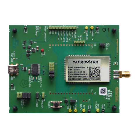
This smart nanoLOC AVR Module is only 35 mm by 14 mm and less than 3 mm thick. Yet it inte-
grates all the required components for a complete RF module based on Nanotron’s innovative
nanoLOC TRX Transceiver. As well as the nanoLOC chip, this module includes the Atmel AVR
ATmega644V microcontroller, a band pass filter, a balun, and an integrated 2.4 GHz chip antenna.
Figure 1: nanoLOC AVR Module
Figure 2: nanoLOC AVR Module - components side
Figure 3: nanoLOC AVR Module - pad side
1.1 Certification
The nanoLOC AVR Module has been certified for use in Europe (R&TTE), Japan (ARIB-T66), and
the United States (FCC).
36 module pins:
16 digital IOs, 2
analog inputs,
PWM, µc reset,
USART, antenna
and TX/RX
Crystals Balun
Band pass
Filter
AntennananoLOC chipMicrocontrollerPin 1
Pin 36
JTAG pins
SPI pins
Pin 1
Pin 36
Scale 3:1
35.05 mm
13.97 mm

Overview
nanoLOC AVR Module User Manual (UserMan)
Page 2 NA-08-0195-0051-1.00 © 2008 Nanotron Technologies GmbH.
1
1.2 Key Components
Table 1: Key components
Component Description
nanoLOC TRX
Transceiver
nanoLOC supports a freely adjustable center frequency with 3 non-overlapping fre-
quency channels within the 2.4 GHz ISM band. This provides support for multiple
physically independent networks and improved coexistence performance with existing
2.4 GHz wireless technologies. Data rates are selectable from 2 Mbps to 125 kbps.
Due to the chip’s unique chirp pulse, adjustment of the antenna is not critical. This sig-
nificantly simplifies the system’s installation and maintenance (“pick and place”).
A sophisticated MAC controller with CSMA/CA and TDMA support is included, as is
Forward Error Correction (FEC) and 128 bit hardware encryption. To minimize soft-
ware and microcontroller requirements, nanoLOC also provides scrambling, automatic
address matching, and packet retransmission.
Integrated into the nanoLOC TRX Transceiver is the DDDL, a Digital Dispersive Delay
Line which is responsible for distinguishing between two possible incoming signals that
are generated by another nanoLOC chip. This received signal is either an Upchirp, a
Downchirp, or a folded pulse (an Upchirp and a Downchirp at the same time). All of
these signals have the same center frequency and the same bandwidth. The differ-
ence between an Upchirp and a Downchirp occurs only in the phase information of the
complex spectrum. This phase information is enough for the DDDL to compress a
pulse at one output port and expand it at the other (that is, to extend the incoming sig-
nal to the doubled duration). In this way the DDDL acts like a matched filter for one of
the possible transmitted pulses.
For more details see nanoLOC TRX Transceiver (NA5TR1) Datasheet available from
Nanotron.
Atmel AVR
ATmega644V
microcontroller
This is a low power CMOS 8-bit microcontroller based on the AVR enhanced RISC
architecture with 64 Kb Flash, 4 Kb SRAM, and 2 Kb EEPROM. This microcontroller
drives the nanoLOC chip via the SPI interface and operates between 1.8 V and 5.5 V.
For more details, refer to the Atmel ATmega644V Datasheet available from Atmel.
Matching circuits
(Balun)
At the RF interface of the nanoLOC chip, a differential impedance of 200 Ωexists
which is matched to the asymmetrical 50 Ωimpedance of the antenna port by a 200 /
50 RF balun. Additional external components at the RF interface have a power and
noise matching function that allows a sharing of the antenna without an external RX/
TX – RF switch.
Integrated 2.4 GHz
chip antenna
As well as this integrated antenna, an external 2.4 GHz antenna can also be con-
nected to the module.
ISM band pass
filter
For an improved robustness against out of band inferences, an ISM band pass filter is
connected at the antenna port.
32.768 kHz,
16 MHz, and
32 MHz quartz
crystals
The 32.768 kHz Quartz is used for the Real Time Clock oscillator. The 16 MHz Quartz
is used by the ATmega microcontroller, while the 32 MHz Quartz works with the inter-
nal oscillator circuitry of the nanoLOC chip.
Connectors
The nanoLOC AVR Module is programmable over JTAG or SPI interfaces. 36 periph-
eral module pins in total are provided, with 16 programmable digital IOs and 2 analog
inputs. The module also provides a pulse-width modulation (PWM) output, a microcon-
troller reset input, a Universal Synchronous RX/TX (USART) input/output, and a TX/
RX signal that enables an external PA.

Absolute Maximum Ratings
nanoLOC AVR Module User Manual (UserMan)
© 2008 Nanotron Technologies GmbH. NA-08-0195-0051-1.00 Page 3
2
2 Absolute Maximum Ratings
Note: It is critical that the ratings provided in Absolute Maximum Ratings be carefully observed.
Stress exceeding one or more of these limiting values may cause permanent damage to the
device.
Table 2: Absolute maximum rating
Parameter Value Unit
Min. operating temperature -40 °C
Max. operating temperature +85 °C
Max. supply voltage (VCC) 2.7 V
Max. DC current per I/O pin 40 mA
Voltage on /RESET with respect
to GND -0.5 to 13.0 V

Electrical Characteristics
nanoLOC AVR Module User Manual (UserMan)
Page 4 NA-08-0195-0051-1.00 © 2008 Nanotron Technologies GmbH.
3
3 Electrical Characteristics
3.1 General / DC Parameters
3.2 RF Parameters
Table 3: General / DC-Parameters
Symbol Parameter Condition Min. Typ. Max. Units
Top Operating
temperature –-40 –+85 °C
Vcc Supply voltage
fcpu does not exceed rec-
ommended value at given
supply voltage1
1. The ATmega644V microcontroller specifies a maximum CPU clock frequency against supply for
safe voltage operation. For more information, see Atmel ATmega644V Microcontroller Datasheet
(2593L–AVR–02/07) on page 318.
2.3 –2.7 V
Icc Supply current no external connections
besides power supply – – 100 mA
VIL Input low voltage VCC = 2.3V - 2.4V
VCC = 2.4V - 2.7V
-0.5
-0.5 –0.2Vcc
0.3Vcc V
VIH Input high voltage VCC = 2.3V - 2.4V
VCC = 2.4V - 2.7V
0.7Vcc
0.6Vcc –Vcc+0.5
Vcc+0.5 V
Table 4: RF parameters
Symbol Parameter Condition Min. Typ. Max. Units
Zant Line impedance of antenna sig-
nal ANT – – 50 –Ω
Rdata Data rate –125 –2000 kb/s
Psens Receiver sensitivity – – – -971
1. The displayed value is the minimum receive signal power required for BER = 10e-3, which is
equivalent to the maximum receiver sensitivity.
dBm
Ptx Transmit power –-33 – 0 dBm

Module Layout
nanoLOC AVR Module User Manual (UserMan)
© 2008 Nanotron Technologies GmbH. NA-08-0195-0051-1.00 Page 5
4
4 Module Layout
4.1 Measures
Figure 4: nanoLOC AVR Module - measures
Figure 5: nanoLOC AVR Module – measures SPI pads (top side)
4.2 Pin Layout
Figure 6: Pin layout - top view
Figure 7: Pin layout - bottom view (inverted)
Unit = mm
Scale 3:1
1.1
35.05
13.97
3.81
10.29
2.03
2.79
2.92
14.61
15.62
Unit = mm
Scale 3:1
1516171819202122232425262728
13
14
12345678910 1112
29
30
31
32
33
34
35
36
SPI4
SPI3 SPI2
SPI1
12345678910 1112
13
14
1516171819202122232425262728
29
30
31
32
33
34
35
36
J1
J10
J5J11
J12
J8
J6
J9
J2
J4
J3 J7 SPI Pins
JTAG Pins

Module Layout
nanoLOC AVR Module User Manual (UserMan)
Page 6 NA-08-0195-0051-1.00 © 2008 Nanotron Technologies GmbH.
4
4.3 Pin Description
Table 5: Pin description
Pin Signal Description Direction
1DIGIO1 Digital general purpose microcontroller port input/output
2DIGIO2 Digital general purpose microcontroller port input/output
3DIGIO3 Digital general purpose microcontroller port input/output
4DIGIO4 Digital general purpose microcontroller port input/output
5GND Ground connection –
6DIGIO5 Digital general purpose microcontroller port input/output
7DIGIO6 Digital general purpose microcontroller port input/output
8DIGIO7 Digital general purpose microcontroller port input/output
9DIGIO8 Digital general purpose microcontroller port input/output
10 GND Ground connection –
11 GND Ground connection –
12 GND Ground connection –
13 GND Ground connection –
14 GND Ground connection –
15 ANT Antenna signal (output) input/output
16 GND Ground connection –
17 GND Ground connection –
18 TX_RX Control signal for external PA output
19 /RESET Reset-Signal for microcontroller input
20 DIGIO9 Digital general purpose microcontroller port input/output
21 DIGIO10 Digital general purpose microcontroller port input/output
22 DIGIO11 Digital general purpose microcontroller port input/output
23 DIGIO12 Digital general purpose microcontroller port input/output
24 GND Ground connection input/output
25 DIGIO13 Digital general purpose microcontroller port input/output
26 DIGIO14 Digital general purpose microcontroller port input/output
27 DIGIO15 Digital general purpose microcontroller port input/output
28 DIGIO16 Digital general purpose microcontroller port input/output
29 GND Ground connection –
30 AIN1 10-bit ADC (Channel 0) input
31 AIN2 10-bit ADC (Channel 1) input
32 PWMOUT PWM signal output
33 VCC Positive supply voltage input
34 RXD UART receive signal input
35 TXD UART transmit signal output
36 GND Ground connection –

Module Layout
nanoLOC AVR Module User Manual (UserMan)
© 2008 Nanotron Technologies GmbH. NA-08-0195-0051-1.00 Page 7
4
4.4 Pins for SPI Programming
4.5 Pins for JTAG Programming
Table 6: Pins for SPI programming
Pin Signal Description Direction
J12 SPISSN SPI Slave Selected; Active Low Digital Input
J8 SPICLK SPI Clock Digital Input
J5 SPIRXD SPI Receive Data (MOSI) Digital Input
J10 SPITXD SPI Transmit Data (MISO) Digital Output
J1 PONRESET Power on reset signal Digital Input
J11 VCCAT Microcontroller supply voltage
Note: pin 33 (VCC) can also be used. –
J4 GND Ground connection –
Table 7: Pins for JTAG programming
Pin Signal Description Direction
J3 /RESET Microcontroller reset Digital Input
J7 TMS Test Mode Select Input Digital Input
J4 GND Ground connection –
J2 TDI Test Data Input Digital Input
J9 TDO Test Data Output Digital Output
J6 TCK Tes t C l ock Digital Output
J11 VCCAT Microcontroller supply voltage –

Soldering Information
nanoLOC AVR Module User Manual (UserMan)
Page 8 NA-08-0195-0051-1.00 © 2008 Nanotron Technologies GmbH.
5
5 Soldering Information
5.1 Recommended Temperature Profile for Lead Free Reflow Soldering
Figure 8: Recommended soldering temperature profile
5.2 Recommended Foot Pattern
The same dimensions for the solder paste screen are recommended, depending on the solder
screen thickness.
Figure 9: nanoLOC AVR Module – recommended foot pattern
Te m p [ ° C ]
150 °C
BD
230°C to 250°C
220 °C
Time [s]
Room Temperature
Pre-heating CoolRamping Reflow
A Temperature
ramping rate:
1 to 7°C/s
B Pre-heating
temperature: 90 ± 30 s
C Temperature
ramping rate:
1 to 7°C / s
D Reflow time: 30 +20/-10 s
AC
190 °C
Ramping
35.05
27.69
26.04
17.02
15.37
13.72
12.07
10.41
8.76
7.11
5.46
3.81
13.97
2.16
12.7
11.05
9.4
7.75
6.1
4.44
2.79
1.14
33.53
31.24
29.59
27.94
26.29
15.37
13.72
12.06
18.41
8.76
7.11
5.46
3.81
2.16
5.84 1.27
1.27
2.54
1.27
1.27
2.54
1.27
0.8
1.4
1.14
10.15
11.8
8.76
5.21
8

Schematics
nanoLOC AVR Module User Manual (UserMan)
© 2008 Nanotron Technologies GmbH. NA-08-0195-0051-1.00 Page 9
6
6 Schematics
Figure 10: nanoLOC AVR Module – schematics 1 of 3

Schematics
nanoLOC AVR Module User Manual (UserMan)
Page 10 NA-08-0195-0051-1.00 © 2008 Nanotron Technologies GmbH.
6
Figure 11: nanoLOC AVR Module – schematics 2 of 3

Schematics
nanoLOC AVR Module User Manual (UserMan)
© 2008 Nanotron Technologies GmbH. NA-08-0195-0051-1.00 Page 11
6
Figure 12: nanoLOC AVR Module – schematics 3 of 3

PCB Layout
nanoLOC AVR Module User Manual (UserMan)
Page 12 NA-08-0195-0051-1.00 © 2008 Nanotron Technologies GmbH.
7
7 PCB Layout
Figure 13: nanoLOC AVR Module – top side
Figure 14: nanoLOC AVR Module – bottom side (inverted)
Figure 15: nanoLOC AVR Module – components top side
Scale 3:1
Scale 3:1
Scale 3:1

Bill of Materials
nanoLOC AVR Module User Manual (UserMan)
© 2008 Nanotron Technologies GmbH. NA-08-0195-0051-1.00 Page 13
8
8 Bill of Materials
Table 8: nanoLOC AVR Module – bill of materials
Part Manufacturer
Description Label Value Qty Package Company Product Number
Antenna ANT1 WE-
7488930245 1WE-
ANT30245
Würth-
Elektronik WE-7488930245
Balun BALUN1 WE-748422245 1 SMD0805 Würth-
Elektronik WE-748422245
Bandpass filter BPF1 WE-BPF1008 1SMD1008 Würth-
Elektronik WE-748351124
Capacitors C28 1.2pF 1SMD0402 Kemet C0402C129C5GAC
C1, C5, C6,
C14, C17,
C19, C27,
C44, C48,
C49, C50,
C51
100nF 12 SMD0402 Phycomp 2238 787 19849
C2, C3, C8,
C13, C16,
C18, C52
100pF 7SMD0402 Phycomp 2238 587 15609
C12, C15 18pF 2SMD0402 Kemet C0402C180D5GAC
C4 1nF 1SMD0402 Phycomp 2238 587 15623
C7, C9, C24,
C25 22pF 4SMD0402 Phycomp 2238 869 15229
C20 33pF 1SMD0402 Phycomp 2238 869 15339
C22, C23 5.6pF 2SMD0402 Kemet C0402C569C5GAC
C21, C26 n.b. 3SMD0402
ICs IC2 ATmega644V-
10MU 1
44M1 Micro
Lead Frame
Package
Atmel ATmega644V-10MU
IC1 NA5TR1 1NA5TR1_
THERM ST NA5TR1
Inductors L5 2.7nH 1SMD0402 Würth-
Elektronik WE-744784027
L6 3.3nH 1SMD0402 Würth-
Elektronik WE-744784033
L1 3.9nH 1SMD0402 Würth-
Elektronik WE-744784039
L3 5.6nH 1SMD0402 Würth-
Elektronik WE-744784056
L2, L4 8.2nH 2SMD0402 Würth-
Elektronik WE-744784082
L7 2200nH 1SMD0603 Murata LQM18NN2R2K00D
PCB P165 1 – Würth-
Elektronik WE-7488930245

Ordering Information
nanoLOC AVR Module User Manual (UserMan)
Page 14 NA-08-0195-0051-1.00 © 2008 Nanotron Technologies GmbH.
9
9 Ordering Information
To order the product described in this document, use the following information.
Quartz crystals Q4 16.000MHz 1
SMD03025/
4
16.000MHz
30/30/-
40+85/12pF
Petermann-
Technik –
Q2 32.000MHz 1
SMD03025/
4
32.000MHz
10/20/-
40+85/
12pF/40R
Petermann-
Technik –
Q1 32.768kHz 1
QUARTZ_3
1SMX-
31M327(H)
SMI 31M327(H)-C
Resistor R1 10k, 1% 1SMD0402 Phycomp 232270671003
Resistor R5,R6,R9 n.b. 3SMD0402 Tyco Electron-
ics
Resistor R4,R7 0Ohm 2SMD0402 Tyco Electron-
ics CRG0402ZR
Resistor R2,R3,R8 1M 3SMD0402 Tyco Electron-
ics CRG0402J1M0-10
Resistor array RA1 1M 14R_ARRAY Phycomp 235003311105
Table 8: nanoLOC AVR Module – bill of materials
Part Manufacturer
Description Label Value Qty Package Company Product Number
Table 9: nanoLOC AVR Module ordering Information
Part Description Part Number Additional Information
nanoLOC AVR Module MN0501AVR nanoLOC Development Kit also available.

Revision History
nanoLOC AVR Module User Manual (UserMan)
© 2008 Nanotron Technologies GmbH. NA-08-0195-0051-1.00 Page 15
Revision History
Version Date Description/Changes
1.0 TBD Initial version.

About Nanotron Technologies GmbH
nanoLOC AVR Module User Manual (UserMan)
Page 16 NA-08-0195-0051-1.00 © 2008 Nanotron Technologies GmbH.
About Nanotron Technologies GmbH
Nanotron Technologies GmbH develops world-class wireless products for demanding applications based
on its patented Chirp transmission system - an innovation that guarantees high robustness, optimal use of
the available bandwidth, and low energy consumption. Since the beginning of 2005, Nanotron's Chirp tech-
nology has been a part of the IEEE 802.15.4a draft standard for wireless PANs which require extremely
robust communication and low power consumption.
ICs and RF modules include nanoNET TRX Transceiver, nanoLOC TRX Transceiver, and ready-to-use or
custom wireless solutions. These include, but are not limited to, industrial monitoring and control applica-
tions, medical applications (Active RFID), security applications, and Real Time Location Systems (RTLS).
nanoNET is certified in Europe, United States, and Japan and supplied to customers worldwide.
Headquartered in Berlin, Germany, Nanotron Technologies GmbH was founded in 1991 and is an active
member of IEEE and the ZigBee alliance.
Further Information
For more information about this product and other products from Nanotron Technologies, contact a sales
representative at the following address:
Nanotron Technologies GmbH
Alt-Moabit 60
10555 Berlin, Germany
Phone: +49 30 399 954 - 0
Fax: +49 30 399 954 - 188
Email: [email protected]
Internet: www.nanotron.com
Table of contents
Other Nanotron Technologies Control Unit manuals