Nepes NM500 User manual

NM500
User’s Manual
NeuroMem chip, 576 neurons
Version 1.6.3
Revised 04/18/2019

NM500 Manual 2
NM500 is a product manufactured exclusively by nepes (www.nepes.kr).
NM500 is subject to a license from General Vision for the NeuroMem® technology.
This manual is published and copyrighted by General Vision Inc. All rights reserved.
For information about the NeuroMem® digital neuromorphic technology, refer to the General Vision web site at
www.general-vision,com and in particular the NeuroMem Technology Reference Guide.

NM500 Manual 3
CONTENTS
1Overview................................................................................................................................................................4
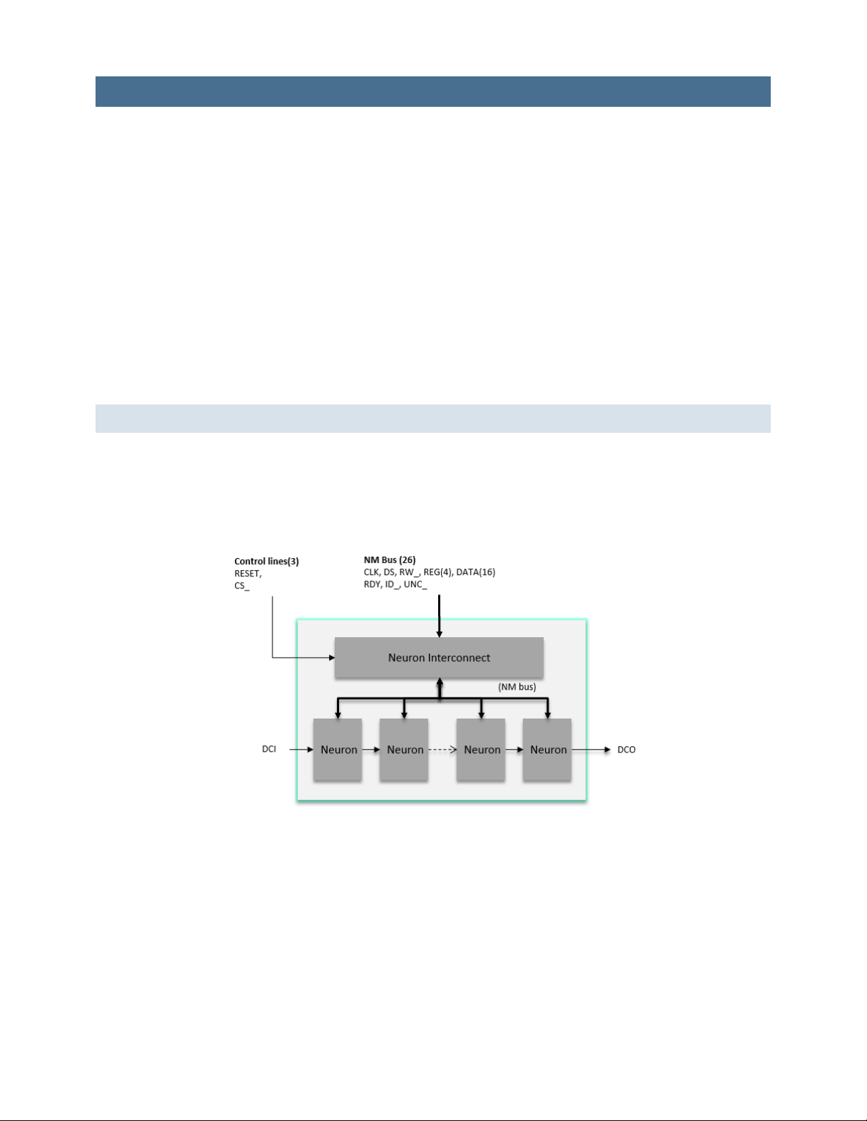
1.1 Architecture .................................................................................................................................................4
1.2 The basic neuron entity................................................................................................................................5
2The control registers..............................................................................................................................................6
2.1 Neuron registers in detail.............................................................................................................................7
2.2 Registers Access Latency............................................................................................................................11
2.3 Typical latencies per operation ..................................................................................................................12
3NeuroMem bus and control lines........................................................................................................................13
3.1 Clocks, power-up and reset........................................................................................................................14
3.1.1 G_Reset, global reset .............................................................................................................................14
3.1.2 G_CLK, system clock ..............................................................................................................................14
3.1.3 CS_, power saving control line...............................................................................................................14
3.1.4 DCI..........................................................................................................................................................14
3.1.5 DCO ........................................................................................................................................................14
3.2 NeuroMem bus ..........................................................................................................................................15
3.2.1 DS...........................................................................................................................................................15
3.2.2 RW_ .......................................................................................................................................................15
3.2.3 REG[3:0] .................................................................................................................................................15
3.2.4 DATA[15:0].............................................................................................................................................16
3.2.5 RDY.........................................................................................................................................................16
3.2.6 ID_..........................................................................................................................................................16
3.2.7 UNC_ ......................................................................................................................................................16
4Typical Timings Constraints .................................................................................................................................17
4.1 Timings .......................................................................................................................................................17
4.2 Learn a vector.............................................................................................................................................18
4.3 Recognize a vector .....................................................................................................................................19
5Interconnecting chips ..........................................................................................................................................20
5.1 Counting the neurons in a chain of unknown length.................................................................................20
5.2 Verifying the proper interconnectivity of the entire chain ........................................................................20
5.3 If a chain has more than 65535 neurons....................................................................................................21
5.4 Single or multiple chains of neurons..........................................................................................................21
6Pinout ..................................................................................................................................................................22
7Mechanical specifications....................................................................................................................................25
8Electrical Specifications .......................................................................................................................................26
8.1 Recommended Operating Conditions........................................................................................................26
8.2 DC Electrical Charateristics.........................................................................................................................26
9Power Consumption ............................................................................................................................................27
9.1 Peak Power.................................................................................................................................................27
9.2 Intrinsic Power ...........................................................................................................................................27
9.3 UPower saving tips ......................................................................................................................................27
10 FAQ ......................................................................................................................................................................28
10.1 Hardware questions ...................................................................................................................................28
10.2 Functional questions ..................................................................................................................................28
10.3 What is the difference between CM1K and NM500 ..................................................................................29

NM500 Manual 4
1OVERVIEW
The NM500 chip is a fully parallel silicon neural network: it is a chain of identical elements (i.e. neurons) addressed
in parallel and which have their own “genetic” material to learn and recall patterns without running a single line of
code and without reporting to any supervising unit. In addition, the neurons fully collaborate with each other
through a bi-directional and parallel neuron bus which is the key to accuracy, adaptivity and speed performance.
Indeed, each neuron incorporates information from all the other neurons into its own learning logic and into its
response logic.
The neurons can learn and recognize input vectors autonomously and in parallel. If several neurons recognize a
pattern (i.e. “fire”), their responses can be retrieved automatically in increasing order of distance (equivalent to a
decreasing order of confidence). The information which can be read from a firing neuron includes its distance,
category, and neuron identifier. If the response of several or all firing neurons is polled, this data can be
consolidated to make a more sophisticated decision weighing the cost of uncertainty or else.
1.1 ARCHITECTURE
The NM500 chip has a unique homogeneous architecture:
-Chain of identical neurons, daisy-chained Intra-Chip and Inter-Chip
-Neuron Interconnect module (switches, no controller or supervisor) which synchronize communication
between the neurons Intra-Chip and Inter-Chip.
-All neurons have the same behavior and execute the instructions in parallel independent from the cluster
or even chip they belong to.
-Selection of one out of two classifiers: K-Nearest Neighbor (KNN) or Radial Basis Function (RBF) and more
precisely a Restricted Coulomb Energy (RCE) neural network
-Recognition time is independent of the number of neurons in use
-Automatic model generator built into the neurons
-Save and Restore of the contents of the neurons
-Simple Register Transfer Level instruction set through of 15 registers

NM500 Manual 5
1.2 THE BASIC NEURON ENTITY
The neuron cell is composed of a memory, a set of 6 registers and some logic gates. For details, please refer to
chapter 3 of the NeuroMem technology Reference Guide.
- Context register: input describing the type of pattern stored in the neuron
- Memory holds a model or prototype
- Category register: input written during a learning operation (whether supervised or unsupervised)
- Distance: output given the distance between an input pattern and the pattern stored in the Memory of
the neuron
- AIF: Active Influence Field auto-adjusted by the neuron
- MINIF: Minimum influence field of the neuron
- Identifier: Position of the neuron in the chain of neurons available
A neuron is said committed when it stores a pattern to its memory along with a category with a value different
from 0. Such action takes place when a learning operation is executed and none of the presently committed
neurons recognize the pattern with a category equal to the category to learn.

NM500 Manual 6
2THE CONTROL REGISTERS
The entire neural network whether composed of one or multiple chips can be used under 2 different modes:
Normal mode
The neurons can learn and recognize patterns. In recognition, the neurons can behave as a K-Nearest Neighbor
(KNN) or Radial Basis Function (RBF) and more precisely a Restricted Coulomb Energy (RCE) neural network.
Save-and-Restore (SR) mode
The neurons become dummy memories which can be read or written. Their automatic model generator and
search-and-sort logic are disabled. The contents of the committed neurons is a representation of the knowledge
they have built autonomously by learning examples. The SR mode allows to view, save and restore this knowledge.
NeuroMem Registers and Read/Write access under the Normal and SR mode.
Abbreviation
Description
Addr 8-bit
Normal mode
SR mode
16-bit default
NSR
Network Status Register
0x0D
RW
W
0x0000
GCR
Global Control Register
0x0B
RW
0x0001
MINIF
Minimum Influence Field
0x06
RW
RW
0x0002
MAXIF
Maximum Influence Field
0x07
RW
0x4000
NCR
Neuron Context Register
0x00
RW
0x0001
COMP
Component
0x01
W
RW
0x0000
LCOMP
Last Component
0x02
W
0x0000
INDEXCOMP
Component index
0x03
W
W
0x0000
DIST
Distance register
0x03
R
R
0xFFFF
CAT
Category register
0x04
RW
RW
0xFFFF
AIF
Active Influence Field
0x05
RW
0x4000
NID
Neuron Identifier
0x0A
R
R
0x0000
POWERSAVE
PowerSave
0x0E
W
n/a
FORGET
Forget
0x0F
W
n/a
NCOUNT
Count of committed neurons
0x0F
R
R
0x0000
RESETCHAIN
Points to the first neuron
0x0C
W
n/a
TESTCOMP
Test Component
0x08
W
0x0000
TESTCAT
Test Category
0x09
W
0x0000
The typical programming sequences to use the neurons are summarized below and described in detail in the
NeuroMem Technology Reference Guide.
https://www.general-vision.com/documentation/TM_NeuroMem_Technology_Reference_Guide.pdf
-Broadcast a vector to all the neurons (whether to learn or recognize it)
-Recognize the last broadcasted vector
-Learn the last broadcasted vector
-Save the content of all the neurons
-Read the content of a specific neuron
-Load the content of the neurons

NM500 Manual 7
2.1 NEURON REGISTERS IN DETAIL
Abbreviation
Register
Normal mode
SR mode
NSR
Network Status Register
Bit[1:0], reserved
Bit[2], UNC (Uncertain)
Bit[3], ID (Identified)
Bit[4], SR mode
Bit[5], KNN classifier
The ID and UNC bits are updated
internally after each Write Last
Comp command.
ID is high if all firing neurons
report the same category.
UNC is high if several neurons fire
but disagree with the category.
Note that this is always the case if
the mode is KNN and 2 committed
neurons have different categories.
KNN is a recognition mode and
should not be active while
learning. Indeed, any pattern
would be recognized whatever its
distance from a neuron and the
learning will only create a single
neuron per new category.
Writing Bit 4 to 1 switches
the chain of neuron to SR
mode and points directly
to the RTL neuron.
GCR
Norm + Context and also
partial identifier of the RTL
neuron
Bit [6:0]= Context
Bit[7]= Lsup Norm
Bit[23:16]= Identifier[23:16]
Global Context assigned to all
neurons not already committed
If the Norm is not set to LSUP, the
default is the L1 Norn or
Manhattan distance.
Accessing the 3rd upper byte of the
RTL neuron is needed if the chain
of neurons is larger than 65535
neurons.
Read as 0xFFFF if the network is
full
N/A
MINIF
Minimum Influence Field
Global MINIF assigned to the non-
committed neurons
Read as 0xFFFF if the network is
full
MINIF of the pointed
neuron, assigned at the
time it was committed
MAXIF
Maximum Influence Field
Global MAXIF assigned to the non-
committed neurons
Read as 0xFFFF if the network is
full
N/A

NM500 Manual 8
Abbreviation
Register
Normal mode
SR mode
NCR
Neuron Context Register
Bit[15:8]=0x00
Bit[7:0]= Identifier [23:16] of the
RTL neuron
Context of the pointed
neuron
Bit[15:8] = Identifier
[23:16]
Bit[7]= LSUP Norm
Bit[6:0]= Context [0, 127]
COMP
Component
Bit[15:8] = unused
Bit[7:0]= byte component
Each Write COMP stores the
component at the current
INDEXCOMP value and updates
the DIST register of the committed
neurons with NCR=GCR and also of
the RTL neuron. INDEXCOMP is
automatically incremented.
After each Read or Write,
moves to the next
INDEXCOMP of the
pointed neuron
LCOMP
Last Component
Bit[15:8] = unused
Bit[7:0]= byte component
Write LCOMP stores the
component at the current
INDEXCOMP value and updates
the DIST register of the committed
neurons with NCR=GCR and also of
the RTL neuron. INDEXCOMP is set
to 0.
The ID_ and UNC_ lines are
updated to report the recognition
status. If ID_ line is low, the
“identified category” is available
on the DATA bus.
N/A
INDEXCOMP
Component index
Common index pointing to
the neurons’ memory
between [0, 255].
Write INDEXCOMP moves to a
specific index value, but does not
reset the DIST register.
This value is incremented
automatically after each Read
COMP or Write COMP. It is reset
after a Write LCOMP.

NM500 Manual 9
Abbreviation
Register
Normal mode
SR mode
DIST
Distance register
between [0, 65535]
DIST=0 means that the
vector matches exactly the
model of the firing neuron.
The higher the distance, the
farther the vector from the
model.
This register is updated by the
neuron during the broadcast of
components (Write COMP and
Write LCOMP)
Read DIST returns the distance of
the top firing neuron. This
“winner” neuron pulls out of the
race, so the next Read Dist will ne
answered by the next top firing
neuron, etc.
DIST=0xFFFF means that there are
no more firing neurons.
Must be read after Write LCOMP
and before Read CAT
N/A
CAT
Category register
Bit 15= Degenerated flag
(read-only)
Bits [14:0]= Category value
between 0 and 32766
(0x7FFE)
CAT greater than 32768
means that the responding
neuron is degenerated. The
value must be masked with
0x7FFF to report the
original category of the
neuron.
Write CAT of 0 does not commit a
new neuron, but may force
existing committed neurons to
reduce their influence fields.
Read CAT returns the category of
the top firing neuron
CAT=0xFFFF means that there are
no more firing neurons
Must be read after the DIST
register except if the ID_ line is
low and the NID register does not
need to be read after the CAT
register.
Category of the pointed
neuron
Read or Write CAT
automatically moves to
the next neuron index in
the chain.
AIF
Active Influence Field
This register is updated
automatically by all the firing
neurons during learning
operations (i.e. Write CAT)
Influence field of the
pointed neuron
NID
Neuron Identifier or index
of the neuron in the chain,
starting with the value 1
Bit[15:0]= 2 lower bytes of a
3-bytes neuron identifier.
The upper byte is stored in
the NCR register. Its access
is only necessary when the
chain of neurons is larger
than 65535.
This register is assigned
automatically when the RTL
neuron gets committed after a
Write CAT.
Read NID returns the identifier of
the firing neuron with the least
distance and least category. It
must be read after a Read CAT. (1)
Identifier of the pointed
neuron.
This register is assigned
automatically when the
pointed neuron gets
assigned a category
different from 0 with a
Write CAT.

NM500 Manual 10
Abbreviation
Register
Normal mode
SR mode
POWERSAVE
PowerSave mode
Writing this register resets
the DATA lines to a tri-state
mode and ensures that they
do not draw current from
the pull-up resistors.
FORGET
Uncommit all neurons by
clearing their category
register.
Note that the neuron’s memory is
not cleared, but its index is reset
to point at the first component.
Also reset the MINIF, MAXIF and
GCR to their default values.
N/A
NCOUNT
Count of committed
neurons
Bit[15:0]= 2 lower bytes of
the count
NCOUNT=0xFFFF means that all
neurons of the chain are
committed. If the chain of neurons
is greater than 65535 neurons this
can also means that 65535
neurons are indeed committed.
Reading the upper byte of the NCR
register can extend the count to a
3 bytes value.
Index of the neuron
pointed in the chain.
Write RESETCHAIN points
to the first neuron. If it is
committed, NCOUNT will
be equal 1, otherwise 0.
RESET
CHAIN
N/A
Points to the first neuron
of the chain.
TESTCOMP(2)
For all committed neurons, write
their component pointed by the
current INDEXCOMP with the
same input value.
Refer to paragraph below for use
model.
TESTCAT(2)
Write the same category
to all the neurons. Useful
for test routines to commit
all neurons in one clock
cycle.
Refer to paragraph below
for use model.
(1) If the content of the neurons has been built using their model generator, there should be no occurrences
of firing neurons with the same distance and same category. As a result, reading the NID returns the
identifier of the sole firing neuron. If, on the contrary, the content of the neurons has been loaded in
Save-and-Restore and is such that multiple neurons can fire with the same distance and same category,
NID will return an “irrelevant” value which is the AND of all their identifier.
(2) Usage of the TEST registers: clear the neurons’ memory
-Write NSR 0x10 Set the SR mode
-Write TESTCAT 1 Commit all neurons with a dummy category value of 1
-Write NSR 0x00 Cancel the SR mode, back to normal mode
-For i=0 to 256

NM500 Manual 11
oWrite TESTCOMP=0
oWrite INDEXCOMP i
-Write NSR 0x10 Set the SR mode
-Write TESTCAT 0 Uncommit all the neurons
-Write NSR 0x00 Cancel the SR mode, back to normal mode
2.2 REGISTERS ACCESS LATENCY
Accessing most registers takes a single clock cycle. In Learn and Recognition mode, reading and writing the LCOMP,
DIST and CAT registers can take between 3 and 19 clock cycles depending on the content of the neuron at the time
of the execution. This means that two neurons can execute a same instruction in different number of clock cycles
depending on its status and internal registers’ values. For example, a neuron which does not recognize an input
pattern will execute the RDIST instruction in 1 cycle, when a neuron which recognizes the pattern (i.e. fires) will
participate to the Search and Sort race for up to 16 clock cycles. The Ready line of the chip indicates when all the
neurons have finished the execution of an instruction and can receive a new one.
Write LCOMP (0x02), Read DIST (0x03), Read and Write CAT (0x04) are "snooping" commands meaning they are
making open collector bus mixing. The release of the DATA lines as well as the ID_ and UNC_ lines after the fall of
the DS signal is critical so they can snoop properly.
The following table reports the number of clock cycles (cc) necessary to read and write the registers of the chip.
The cycles are counted from the first rising edge of the system clock upon the receipt of the DS signal, to the rising
edge of the READY signal upon execution of the command.
Addr
Register
Description
Learn and Recognition
mode
Save and Restore
mode
Write cycles
Read
cycles
Write
cycles
Read
cycles
0x00
NCR
Neuron Context Register
1
1
0x01
COMP
Component
1
1
1
0x02
LCOMP
Last Component
1 if no neurons
3 otherwise
0x03
0x03
INDEXCOMP
DIST
Component Index
Distance
1
18
1
1
0x04
CAT
Category
1 if ID, 19
otherwise
3 if ID, 19
otherwise
1
1
0x05
AIF
Active Influence Field
1
1
0x06
MINIF
Minimum Influence Field
1
1
1
0x07
MAXIF
Maximum Influence Field
1
1
0x08
TESTCOMP
Test Component
1
0x09
TESTCAT
Test Category
1
0x0A
NID
Neuron Identifier
1
1
0x0B
GCR
Global Context Register
1
1
0x0C
RESETCHAIN
1
0x0D
NSR
Network Status Register
1
1
0x0F
FORGET
Clear the neurons
1
0x0F
NCOUNT
Committed neurons
1
1

NM500 Manual 12
2.3 TYPICAL LATENCIES PER OPERATION
Operation
Clock cycles
@35 Mhz (single chip)
L=256, N=576, K=3
@18 Mhz (multi-chips)
L=256, N=576, K=3
Broadcast a vector of Length L
L+3
7.3 µs
14.3 µs
Learn a vector of length L
L+3 + 18
7.9 µs
15.4 µs
Status of a vector of length L
L+3+1
7.4 µs
14.4 µs
Best match of a vector of length L
L+3+37
8.3 µs
16.2 µs
Get the K top match of a vector of length L
L+3+ (K*37)
9.1 µs
17.8 µs
Save N neurons
4+ (N*260)
4.27 ms
8.3 ms
Restore N neurons
4+ (N*260)
4.27 ms
8.3 ms

NM500 Manual 13
3NEUROMEM BUS AND CONTROL LINES
This chapter describes the NeuroMem buses and control lines:
Symbol
Type
Description
Configuration lines
VCC
Core power supply (1.2v)
VCCIO
IO power supply line (3.3 v)
GND
Ground line
DCI
Input
Daisy Chain In
DCO
Output
Daisy Chain Out
Clock and Reset
G_CLK
Input
System clock
G_RESET_
Input
Hardware reset
CS_
Input
Enable chip activity
NeuroMem bus
DS
Input
Data strobe line
R/W_
Input
Read/Write
REG[0:3]
Input
Register
DATA[0-15]
Bidir
Data
Neuron output lines
ID_
Bidir
Identified_low line
UNC_
Bidir
Uncertain_low line
RDY
Output
Ready line

NM500 Manual 14
3.1 CLOCKS, POWER-UP AND RESET
3.1.1 G_RESET, GLOBAL RESET
The chip is reset at power-up by pulling down the G_RESET_l pin for a minimum of 5 clock cycles. An internal reset
signal is then sustained for 255 clock cycles to filter any bouncing of the G_RESET_l external pulse. It is propagated
internally to the neurons so all registers are set to their default values. In a multi-chip configuration, the same
G_RESET_ must be connected to all chips.
3.1.2 G_CLK, SYSTEM CLOCK
The chip operates at a typical system clock of 35 MHz. If multiple chips are connected in parallel the typical system
clock is 18 Mhz.
3.1.3 CS_, POWER SAVING CONTROL LINE
The CS_ line controls the propagation of the system clock G_CLK to the neurons. It is pulled low by default letting
the clock run continuously.
Pulling up the the CS_ line when the chip is unused reduces considerably its power consumption (from 500 mW to
25 mW).
The timings to pull CS_ down and let the system clock pass through must be accurate:
-It must be pulled down on a negative edge of the clock when the external data strobe (DS) is high.
-It must be released on the negative edge of the clock following the rise of the RDY signal at the earliest.
3.1.4 DCI
Until the DCI line of a chip is high, its neurons are idle. As soon as the DCI line rises, the neurons of the chip
become active, meaning ready to learn and recognize.
In a configuration with multiple chips, the Daisy-Chain-In (DCI) line of the first chip must be high. For the
subsequent chips, the connection between their DCO and DCI lines allows to physically arrange them in a chain.
The DCI line of a chip must be connected to the DCO of the previous chip in the chain. Its status is then controlled
by the neurons of the previous chip.
3.1.5 DCO
The Daisy-Chain-Out (DCO) line of a chip must be connected to the DCI of the next chip in the chain, if applicable. It
is low by default and will rise when the last neuron of the chip gets committed. If this line is connected to the DCI
of another chip, the later will awake its neurons to become Ready-To-Learn.

NM500 Manual 15
3.2 NEUROMEM BUS
The neurons receive instructions simultaneously through a proprietary NeuroMem bus composed of the 26 lines as
described below. The execution of these instructions can take different number of clock cycles per neuron
depending on their status and content (committed and firing, committed and not firing, ready-to-learn or idle) and
their interactions.
The external controller sending Read/Write commands to a chain of chips must be careful to release the
bidirectional lines as soon as the Ready signal falls. Failure to do so will prevent the proper execution of commands
interconnecting all the neurons together through the bi-directional lines of DATA, ID_, and UNC_.
DS Data strobe line
RW_ Read/Write line (default is Read=1)
REG 4 bit register
DATA 16-bit data
RDY Ready control line mixing the RDY output signal of all the neurons in the chain and indicating that the
neurons are all ready to execute a new command
ID_ Control line mixing the ID_ output signal of all the neurons in the chain and indicating that neurons
have identified the last vector and that these neurons are all in agreement for its classification.
UNC_ Control line mixing the UNC_ output signal of all the neurons in the chain and indicating that neurons
have identified the last vector but disagree with its classification. This line is an in/out line because
used as an input during the execution of certain Write register.
3.2.1 DS
The data strobe line, DS, must be asserted and de-asserted at the negative edge of G_CLK. It must be asserted only
when the RDY line is high.
3.2.2 RW_
The Read/Write line, RW_, must be low to write and high to read. It is low by default. This signal is sampled on the
positive edge of G_CLK when DS is high. In the case of a Write command, it must be pulled low only for the
duration of the DS high and then immediately released to allow the interconnectivity of the neurons during a Write
Last Component or a Write Category.
3.2.3 REG[3:0]
The four Register lines, REG, represent the 4-bit address of the register to read or write. They are sampled on the
positive edge of G_CLK when DS is high and must be not be released before the rise of the RDY line.

NM500 Manual 16
3.2.4 DATA[15:0]
The 16 DATA lines are connected to open collectors and can have three different states:
-During a write operation (CM_RW low and DS high), DATA is the 16-bit value to write to the selected
register. It is sampled by the neurons at the positive edge of G_CLK when DS is high and RW is low.
-At the end of a read operation (RW high and RDY rising), DATA is the 16-bit value of the selected register.
It can be read on or after the rising edge of CM_RDY after the fall of DS. The default output value is
0xFFFF.
-During the execution of the commands which last more than one clock cycles, the DATA lines must be
released to allow the mixing and snooping of the responses of all the neurons connected in parallel in a
same chain. These operations are the Write LCOMP, Write CAT, Read DIST and Read CAT.
3.2.5 RDY
The Ready line, RDY, is pulled down by the neurons during the execution of a command and released upon its
termination. It is updated at the positive edge of the system clock G_CLK whether the command is recognized by
the neurons.
3.2.6 ID_
The Identified line, ID_, is pulled down when all the neurons recognizing the last input vector are all in agreement
and return the same category. This line is updated each time the last component of a vector is broadcasted to the
neurons either through a Write LCOMP command. The actual update occurs at the 3rd negative edge of the clock
during the execution of the Write LCOMP. The ID_ line is released at the next Write COMP.
The ID_ line is also continuously latched in bit [3] of the NSR register of the chip at the positive edge of the clock.
3.2.7 UNC_
The Uncertain line, UNC_, line is bidirectional and shall not be driven. It is an output during a recognition operation
and an input during a learning operation.
UNC_ is pulled down when the neurons recognizing the last input vector have different categories. This update
occurs each time a Write LCOMP is executed. The actual update occurs at the 3rd negative edge of the clock during
the execution of the Write LCOMP. The UNC_ line is released at the next Write COMP. Note that UNC_ is always
pulled down if the mode is KNN and 2 committed neurons have different categories.
The UNC_ line is also continuously latched in bit [2] of the NSR register of the chip. at the positive edge of the
clock.
During a Write CAT, this line is asserted by the neurons if the last input vector is recognized as a novelty and must
be stored into a new neuron.

NM500 Manual 17
4TYPICAL TIMINGS CONSTRAINTS
The DS, RW_, REG and DATA signals are updated at the negative edge of the system clock (G_CLK) so that they are
stable when the neurons read them at the next positive edge of G_CLK. The RDY signal is then immediately pulled
down by the neurons and released at the first positive edge of G_CLK following the completion of the command.
The duration during which the RDY signal is low represents the execution time of the command.
In the case of a Read command, the output DATA is ready to be read when RDY rises.
4.1 TIMINGS
All the neurons execute the commands simultaneously. Depending on their status (Idle, Ready-to-Learn or
Committed) and on the register to access, the Read and Write commands can take between 1 and 19 clock cycles.
The neurons sample signals on the positive edge of the system clock G_CLK. Their setup time must be at least 5
nanoseconds before the positive edge of G-Clock. The hold time must be at least 5 nanoseconds after the positive
edge of the clock.
The neurons pull down their RDY line when the DS rises and hold it down for the duration of the command. Upon
completion, the RDY line is pulled back up on the positive edge of the system clock.
The CS_ signal must be pulled down at the latest when the DS signal rises and it can be pulled back up at the
earliest when the RDY line rises back up.
A Write command (DS, RW_=0, REG, DATA) must be stable on the positive edge of the system clock and released
before the next positive edge of the system clock. The DATA lines must be released before the next positive edge
of the clock to ensure that the data bus becomes bi-directional for proper execution of the commands requiring
snooping of the bus.
A Read command (DS, RW_=1, REG) must be stable on the positive edge of the system clock and released before
the next positive edge of the system clock. DATA is stable when the RDY control line is pulled high.
Write in one cycle: REG MINIF (0x06)
Read in one clock cycle: REG CAT (0x04) in SR mode

NM500 Manual 18
Write taking two cycles: REG LCOMP (0x02)
Remark: When the DS signal is asserted the DATA bus must be set the value to write (i.e. 0x000b). It is then
switched to a tri-state mode (i.e. 0xFFFF) during a search and sort between the firing neurons so they can
determine if the input vector is identified (ID_l), uncertain (UNC_l) or unknown.
Read taking sixteen cycles: REG DIST (0x03)
4.2 LEARN A VECTOR
In the example below, a vector of 8 components is learned. The resolution of the diagram does not allow for the
display of the DATA values, but this is not important for understanding the timing constraints of the chip.
The sequence of instructions consists of 7 Write COMP, 1 Write LCOMP, and 1 Write CAT.
When REG is equal to 01, each DS pulse triggers a Write COMP lasting one cycle of G_CLK. The RDY signal has the
same duration as the DS only shifted by one half clock cycle.

NM500 Manual 19
When REG is equal to 02, the DS pulse triggers a Write LCOMP. The RDY signal is pulled down for 3 cycles. The fact
that both lines ID_l and UNC_l are pulled up indicates that the input vector is not recognized by any existing
neuron. The subsequent Write CAT command will necessarily commit a new neuron.
When REG is equal to 04, the DS pulse triggers a Write CAT. The RDY signal is pulled down for 19 cycles.
4.3 RECOGNIZE A VECTOR
The sequence of instructions consists of 7 Write COMP, 1 Write LCOMP, 1 Read DIST and 1 Read CAT.
When REG is equal to 01, each DS pulse triggers a Write COMP. The RDY signal is pulled down for one cycle.
When REG is equal to 02, the DS pulse triggers a Write LCOMP. The RDY signal is pulled down for 3 cycles. The
UNC_l is pulled down at the last negative edge of G_CLK before RDY is pulled back up. This indicates that the input
vector is recognized by more than one neuron and that different categories are identified.
When REG is equal to 03 and RW_l remains high, the DS pulse triggers a Read DIST. The RDY signal is pulled down
for 18 cycles which is the duration of the Search and Sort looking for the firing neuron with the smallest distance
value. This distance is equal to 08.
When REG is equal to 04 and RW_l remains high, the DS pulse triggers a Read CAT. The RDY signal is pulled down
for 19 cycles which is the duration of the Search and Sort looking for the firing neuron with a distance register
equal to 08 and the smallest category value. This category is equal to 01.
Remark: Since it is known that the recognition status is uncertain (UNC_L is low), executing another series of Read
DIST followed by Read CAT would report the distance and category of the next neuron with the smallest distance.

NM500 Manual 20
5INTERCONNECTING CHIPS
One of the benefits of the NM500 architecture is that you can cascade multiple chips in parallel to expand the size
of the neural network by increment of 576 neurons. The behavior of the neurons in a single-chip or multiple-chips
configuration remains the same.
A chain of multiple chips is defined by connecting their NeuroMem bus together with external pull-up resistors
when applicable (refer to the pinout table for details).
The external controller sending Read/Write commands to a chain of chips must be careful to release the
bidirectional lines as soon as the Ready signal falls. Failure to do so will prevent the proper execution of commands
interconnecting all the neurons together through the bi-directional lines of DATA, ID_, and UNC_.
5.1 COUNTING THE NEURONS IN A CHAIN OF UNKNOWN LENGTH
-Write NSR 0x10 Set the SR mode
-Write TESTCAT Value Commit all the neurons with a same category value
-Write RESETCHAIN Point to the 1st neuron in chain
-Ncount=0
-Do Loop
oRead CAT, cat
oNcount++
-Until cat=0xFFFF (Ncount-1) is the number of neurons in the chain
-Write NSR 0x00 Cancel the SR mode
5.2 VERIFYING THE PROPER INTERCONNECTIVITY OF THE ENTIRE CHAIN
When multiple chips are assembled in a chain, their inter-connectivity needs to be verified to ensure proper
learning and recognition. This inter-connectivity depends on mechanical and electrical constraints and this chapter
describes the recommended functional verifications:
Table of contents
Popular Robotics manuals by other brands

Sony
Sony ERS-210 AIBO Dancer operating instructions

adept technology
adept technology Cobra s600 user guide

SuperDroid Robots
SuperDroid Robots IG42-SB4-T manual

TT Robotix
TT Robotix TTR-SB Seawolf instruction manual

De Agostini
De Agostini MODEL SPACE Robi manual

Tinkerbots
Tinkerbots Advanced Robotics Set manual