Nokia RH-42 Guide

CCS Technical Documentation
RH-42 Series Transceivers
Issue 2 09/2003 Confidential Nokia Corporation
Troubleshooting Instructions

RH-42
Troubleshooting Instructions CCS Technical Documentation
Page 2 Nokia Corporation Confidential Issue 2 09/2003

CCS Technical Documentation Troubleshooting Instructions
RH-42
Issue 2 09/2003 Nokia Corporation Confidential Page 3
Contents
Page No
Transceiver Troubleshooting ......................................................................................... 5
Baseband Troubleshooting ..........................................................................................5
General testing........................................................................................................... 5
Troubleshooting ........................................................................................................ 5
Power up faults.......................................................................................................... 6
Flash Programming does not work.......................................................................... 10
Charging .................................................................................................................. 12
Audio failures.......................................................................................................... 13
Accessory detection................................................................................................. 16
Sleep Clock ............................................................................................................. 17
Display/Keyboard lights do not work ..................................................................... 18
Display does not work............................................................................................. 19
Buzzer does not work.............................................................................................. 20
Keyboard does not work ......................................................................................... 20
Receiver Troubleshooting ..........................................................................................20
General instructions for RX troubleshooting .......................................................... 20
Path of the received signal ...................................................................................... 20
Fault-finding charts for receiver chain .................................................................... 21
Transmitter Troubleshooting .....................................................................................24
General instructions for TX troubleshooting .......................................................... 24
Path of the transmitted signall................................................................................. 24
Fault-finding charts for the transmitter ................................................................... 24
Synthesizer Troubleshooting .....................................................................................28
19.44 MHz reference oscillator............................................................................... 28
RX VHF .................................................................................................................. 29
Fault-finding chart for RX VHF VCO ................................................................... 30
TX VHF................................................................................................................... 30
UHF Synthesizer ..................................................................................................... 31

RH-42
Troubleshooting Instructions CCS Technical Documentation
Page 4 Nokia Corporation Confidential Issue 2 09/2003

CCS Technical Documentation Troubleshooting Instructions
RH-42
Issue 2 09/2003 Nokia Corporation Confidential Page 5
Transceiver Troubleshooting
First, carry out a thorough visual check of the module. Make sure that:
• there is no mechanical damage
• the solder joints are OK
Note: Before changing anything, ALL SUPPLY VOLTAGES AND THE SYSTEM CLOCK / SLEEP
CLOCK should be checked.
Baseband Troubleshooting
General testing
The phone has three different modes for testing and/or repairing the phone. The modes
can be selected with suitable resistors connected to BSI- and BTEMP- lines as illustrated
in the following table:
If the corresponding resistors are connected, the MCU software automatically enters into
the local or test mode when the supply voltage is connected to the phone.
The power can be switched on by:
1 Pressing the power key.
2 Connecting the local/test mode resistors to the bsi/btemp lines and connecting
the battery voltage to the phone.
3 Connecting a charger.
4 Phone’s internal functions (Real time clock alarm)
In the local and test mode, the baseband can be controlled through MBUS or FBUS (FBUS
is recommended) connections using Phoenix service software.
Troubleshooting
Note: Most of the baseband repair actions require removing the baseband shield. The shield must not
be removed unless separately authorized by the program.
Note: The phone’s ESN has to re-written to the UEM, if the UEM is replaced. This can be done only in
Central Service.
Mode BSI-resistor BTEMP resistor Remarks
Local mode 0 - 1k 0 - 1k
Test mode >1k 0 - 1k
Normal mode 68k 47k Recommended for baseband
testing. Same as local mode, but
making a phone call is possible.

RH-42
Troubleshooting Instructions CCS Technical Documentation
Page 6 Nokia Corporation Confidential Issue 2 09/2003
The BB troubleshooting instructions consist of the following topics:
1Powerup
2 Flash programming
3Audio
• Earpiece
• Microphone
4 Charging
5 Accessory detection
6 Sleep clock
7 User interface
• Display
• Lights
• Buzzer
• Keyboard
Power up faults
Power up sequence
1 The UEM acts as a HW master during start up
• Vbatt limits: 2.1V for internal state machine, 3V triggering whole startup
• Regulator sequencing
• HW "core" regulators "on": Vio, Vcore, VR3, Vflash1
These regulators supply the processors, memory, chip interfaces and clock source in RF
• Reset releasing delay
• Supply voltages stabilize to their UEM HW default values
• RFCLK grows to full swing
• The core is ready to run but waiting for the PURX release

CCS Technical Documentation Troubleshooting Instructions
RH-42
Issue 2 09/2003 Nokia Corporation Confidential Page 7
• Reset releasing
• The UPP releases the SLEEPX up to the "non sleep" -state to prevent the UEM
switching the regulators "OFF"
2 MCU starts running the Bootsrap Code
• Written in stone/ UPP internal ROM
• The program checks if there is any reason for the FDL mode (Flash Down Load)
• If there is an executable code in FLASH and there is no reason for FDL, the MCU
starts running the MCU program from FLASH.
3 MCU runs the FLASH MCU code
• The phone initialization, user interfaces, internal blocks, etc.
• Core regulator voltage setting for required DSP speed
• Initializes the DSP and concerning HW
• Releases DSP reset -> DSP starts running
Note: In the following figure, the RF_Clk frequency appears to be lower than 19.44 MHz because of a
too low oscilloscope sampling frequency (2kS/s).
Figure 1: Power up sequence

RH-42
Troubleshooting Instructions CCS Technical Documentation
Page 8 Nokia Corporation Confidential Issue 2 09/2003
1 Power key pressed
• After 20ms UEM enters RESET MODE if VBAT>Vmstr+
• VFLASH1, Vana, Vcore, Vio and VR3 goes high.
• VCTCXO enabled by VR3 -> RFClk 19.44 MHz running.
2Purxreleased
• Purx released by UEM, UEMINT goes high for 100 ms, SleepX goes high and
UEM starts feeding SleepClk (32 KHz) to UPP.
Note: The sleepclock starts running in the crystal circuitry (B200) immediately when the battery volt-
age is supplied.
3 Software running
• Default value for Vcore is 1.5 volts when the software is running.
• Cbus (1.08MHz) clock starts running.
Phone does not start up normally or does not stay on
Note: In case of power up faults, it is not possible to force the phone on by disabling the watchdog.
Instead, measurements should be taken immediately when the power key is pressed or when the bat-
tery voltage is connected to the phone (local/test mode).
The easiest way to check if the software is running when the phone takes an abnormal
amount of current is to measure the cbusclk and Vcore.
The Dbus clock (programmable 9.72 MHz) is not automatically visible in the test and
local modes.

CCS Technical Documentation Troubleshooting Instructions
RH-42
Issue 2 09/2003 Nokia Corporation Confidential Page 9
Figure 2: Fault tree, phone does not power up
Check the power key
Try to start phone to
test or local mode
Measure Vflash1,
Vana, Vio, Vcore, VR3
when pwr key pressed
Check R202, R206,
R207, C220, C240
Check X101
Check G790 (missing
or misaligned)
Check
19.44MHz RF
clock from C420
Check C420
Check 19.44MHz from
G790
Check R792, C792,
C793
Change G790Change N801
Measure VBAT from
C261
Change UEM
(D200)
Check that purx goes
up to 1.8V
Measure J406 (it
should be 1.08MHz)
Change
UPP (D400)
Reflash phone
Go to Flash
Failure flowchart
FAIL
OK
OK
OK
FAIL
OK
VANA and VR3 missing
FAIL
FAIL
OK
OK
OK
FAIL
OKOK
FAIL
OK
FAIL
OK
Programming fails
Programming OK but phone doesn't start
OK

RH-42
Troubleshooting Instructions CCS Technical Documentation
Page 10 Nokia Corporation Confidential Issue 2 09/2003
Flash Programming does not work
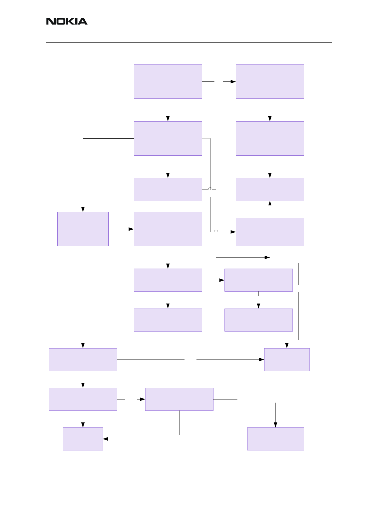
Flash programming procedure
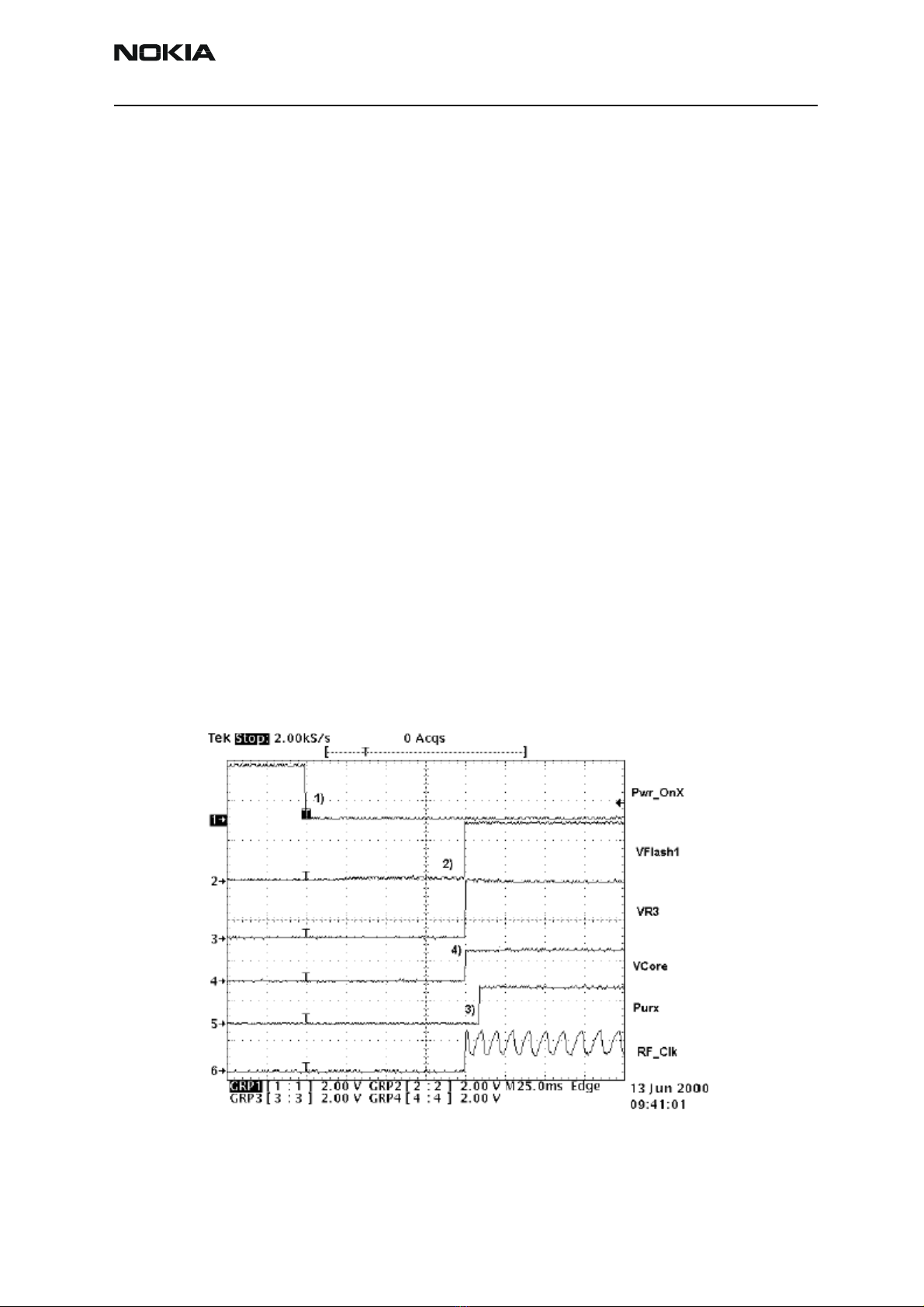
1 The phone communicates with the prommer via the production test pattern,
using the following signals:
• FBUSTX(serial data to phone)
• FBUSRX(serial data from phone)
• MBUS(serial clock for FBUSRX)
• VPP(External flashing voltage for speed up flashing)
The BSI line is also used when initializing flashing (battery connector).
2 When the phone is powered (VBAT>3V), the MBUS and FBUSTX lines are pulled
up internally by the phone.
3 The prommer sends a command to the UEM, using FBUSRX, to enter the Flash-
mode. During the sending of this command, the prommer keeps the BSI line high
and MBUS is used as a serial clock.
4 When the Flash-mode command is acknowledged, UEM enters the Flash-mode
and releases reset (PURX) to MCU.
5 After reset is released, UPP checks if there is a request for the Bootstrap code
(that resides in the UPP ROM).
6 The request for Bootstrap is the MBUS pulled down by the prommer (if the boot-
strap is not requested, the bootstrap code jumps to FLASH SW).
7 If the Bootstrap code is requested, UPP enters the Flash-mode and sets FbusTX to
'0' as an acknowledgement to the prommer. This is an indication that UPP can
run, at least, the fixed Bootstrap code – although it is not able to run the FLASH
code. UPP then sends an UPP-ID to the prommer via the FBUSTX line.
8 After the prommer has received the UPP-ID, it sends a corresponding Secondary
Boot Code to the phone via FBUSRX. The Secondary Boot Code, when run in UPP,
requests UPP to send information to the prommer about the flash type and other
HW-related parameters about the device to be flashed.
9 Prommer then sends the Algorithm Code corresponding to the HW parameters,
and this algorithm, when run in UPP, takes over handling the MCUSW transfer to
Flash.
10 12 volts can be supplied to Vpp (by the prommer) to speed up flashing.

CCS Technical Documentation Troubleshooting Instructions
RH-42
Issue 2 09/2003 Nokia Corporation Confidential Page 11
11 The FLASH Program includes a package of MCU and DSP software and all default
parameters for the phone. The tuning values will be added/rewritten during the
Flash/Alignment phase.
Flash programming error codes
The various error codes can be seen from the FPS-8 Flash in Phoenix.
The underlined text in the table below means that the item under consideration is being
used for the first time in the flashing sequence.
Error Description Not working properly
C101 "The Phone does not set FbusTx line high
after the startup."
Vbatt
Vflash1
Vcore
VIO
BSI and FbusRX from prommer to UEM.
FbusTx from UPP->UEM->Prommer(SA0)
C102 "The Phone does not set FbusTx line low
after the line has been high. The Prommer
generates this error also when the Phone is
not connected to the Prommer."
PURX(also to Taco)
VR3
Rfclock(VCTCXO->Taco->UPP)
Mbus from Prommer->UEM->UPP(MbusRx)(SA1)
FbusTx from UPP->UEM->Prommer(SA1)
C103 "Boot serial line fail." Mbus from Prommer->UEM->UPP(MbusRx)(SA0)
FbusRx from Prommer->UEM->UPP
FbusTx from UPP->UEM->Prommer
C104 "MCU ID message sending failed in the
Phone."
FbusTx from UPP->UEM->Prommer
C105 "The Phone has not received Secondary boot
codes length bytes correctly."
Mbus from Prommer->UEM->UPP(MbusRx)
FbusRx from Prommer->UEM->UPP
FbusTx from UPP->UEM->Prommer
C106 "The Phone has not received Secondary code
bytes correctly."
Mbus from Prommer->UEM->UPP(MbusRx)
FbusRx from Prommer->UEM->UPP
FbusTx from UPP->UEM->Prommer
C107 "The Phone MCU can not start Secondary
code correctly."
UPP
A204 "The flash manufacturer and device IDs in
the existing Algorithm files do not match
with the IDs received from the target
phone."
Flash
Signals between UPP-Flash
A387 "The MCU ID in the MCUSW.” UPP
C601 "The prommer has detected that Vpp voltage
level has dropped below the limit"
Vpp from prommer - >Flash

RH-42
Troubleshooting Instructions CCS Technical Documentation
Page 12 Nokia Corporation Confidential Issue 2 09/2003
Charging
Note: The charging voltage and current can be checked by connecting the phone to the service soft-
ware and reading the ad- converter values of the vchar and ichar.
If charging fails when the LCH-9 is used, and works with ACP-7 and ACP-8, check that
the charge control pin of the system connector is connected to the ground.
C383
C583
C683
"The Prommer has not received Phone
acknowledge to the message."
(C383-during algorithm download to target
phone)
(C583-during erasing)
(C683-during programming)
Flash
UPP
Signals between UPP-Flash
C384
C584
C684
"The Phone has generated NAK signal during
data block transfer."
(C384-during algorithm download to target
phone)
(C584-during erasing)
(C684-during programming)
Flash
UPP
Signals between UPP-Flash
C585
C685
Data block handling timeout"
(C585-during erasing)
(C685-during programming)
Flash
UPP
Signals between UPP-Flash
C586
C686
"The status response from the Phone informs
about fail."
(C586-during erasing)
(C686-during programming)
Flash

CCS Technical Documentation Troubleshooting Instructions
RH-42
Issue 2 09/2003 Nokia Corporation Confidential Page 13
Figure 3: Fault tree, charging
Audio failures
In case of audio failures, there are three possibilities to check the audio lines.
1 Make a phone call against tester and check audios.
2 In case the earpiece/XMIC fails: Feed a 1 Khz signal to the XMIC line and measure
the signal from the earpiece line. The Audio test box (JBA-8) is needed. The Audio
loop (Audio test/Ext In Hp Out) must be switched on by the Phoenix service soft-
ware. This loop will connect audios only through the UEM. In this case, the UPP is
not used.
In case the internal microphone/XEAR fails: Feed the tone to the microphone and mea-
sure the signal from the XEAR line. The Audio test box (JBA-8) is needed. The Audio loop
Phone doesn't
start charging
Connect charger and
check VCHARIN
Check F100, L100,
V100, and C106
Check ICHAR
Check R202, R206,
R207, C201, C202,
C220, C240, and
R200
Change the UEM
Check bottom
connector
-VIN
_Charge control pin
Fail
OK
Fail
OK
OK

RH-42
Troubleshooting Instructions CCS Technical Documentation
Page 14 Nokia Corporation Confidential Issue 2 09/2003
(Audio test/Hp In Ext Out) must be switched on by the Phoenix service software. This loop
will connect audios only through the UEM. In this case, the UPP is not used.
3 Run the audio-loop self-test with Phoenix (BB Self Tests/
ST_EAR_DATA_LOOP_TEST). This loop will test the ear-data/mic-data lines
between the UPP and the UEM.
Earpiece or external microphone line does not work
Figure 4: Fault tree, earpiece failure
Earpiece
doesn't work
R un audio loop s elf-
tes t with P hoenix
Feed 1K Hz to XMIC
by J B A-8 and
measure from
earpiece
Check R 157
Check earpiece
Change UEM
Change UPP
Fail
Fail
OK
OK
OK
OK

CCS Technical Documentation Troubleshooting Instructions
RH-42
Issue 2 09/2003 Nokia Corporation Confidential Page 15
Microphone or XEAR line does not work
Figure 5: Fault tree, microphone failure
Microphone doesn't
work
R un audio loop self-
tes t with P hoenix
Feed 1K Hz to MIC by
J B A-8 and measure
from XE AR
Check R 156, C151,
C152, C 157, L164
Check microphone
Change UEM
Change UPP
Fail
OK
Fail
OK
OK

RH-42
Troubleshooting Instructions CCS Technical Documentation
Page 16 Nokia Corporation Confidential Issue 2 09/2003
Accessory detection
1 Start the phone in the normal mode when checking for accessory detection.
2 The Ad- converter value of the hookint-line can be checked with the Xmic-
switch on an MJS-18 test jig. Changes normally from high to low when no acces-
sory is connected.
3 When the headset (HDC-5) is connected, the hookint- value should be between
600 and 800.
Figure 6: Fault tree, accessory detection
Accessory detection
doesn't work normally
Check Headint ad
value with Phoenix
(no accessory
connected
- Headint ~0 *)
Use XMIC switch on
MJS-18 and check
hookint ad value.
Should go from high
(~1000) to low (~0)
Check R151 and
C160
Check R152, C161,
L160
Check R150, R201,
C104, C106, L162,
L163
Check bottom
connector
Change UEM
* On local or test
mode Headint <400
OK
Fail
OK
OK
OK
OK
OK
Fail

CCS Technical Documentation Troubleshooting Instructions
RH-42
Issue 2 09/2003 Nokia Corporation Confidential Page 17
Sleep Clock
Missing/nonfunctional sleep clock causes
• Entering sleep mode fails (higher current consumption -> shorter standby time).
• Baseband self tests cannot be run.
• Phone clock (on display) does not function properly.
Figure 7: Fault tree, sleep clock
Sleep mode not
working
Measure sleep clock Measure sleep clock
from B200
Check C209 and
C210
Change B200Change UEM (D200)Change UPP (D400)
Fail Fail
OKOKOK

RH-42
Troubleshooting Instructions CCS Technical Documentation
Page 18 Nokia Corporation Confidential Issue 2 09/2003
Display/Keyboard lights do not work
Figure 8: Fault tree, Display/Keyboard lights
Display/Keyboard
lights are not
working
Check R 300
(Display) and R301
(K eyboard)
Replace resistor(s)
Check LEDs
V300...V303 (Dis play)
and V304...V309
(K eyboard)
Replace LED(s)
Use Display Test in
Phoenix to s et lights
ON/OFF
Replace UEM
Fail
OK
Fail
OK
Fail

CCS Technical Documentation Troubleshooting Instructions
RH-42
Issue 2 09/2003 Nokia Corporation Confidential Page 19
Display does not work
Figure 9: Fault tree, Display does not work
Display does not
work
Check that phone
powers up normally
(current
cons umption, power
up sequence)
Proceed toPhone
Doesn't Power Up
troubleshooting
Check display
visually (possible
cracks on COG
driver or glass ,
capacitors loose or
broken)
Replace Display
Module
Check PWB and
elastomer connector
Clean PWB and
replace elas tomer if
needed.
R un LCD test in
Phoenix (BB Self
Tests/
S T_L CD_TE S T)
Check capacitors
C302...C304 R eplace capacitor(s )
Replace Display
Module
R eplace elas tomer
Use Display Test in
Phoenix to check if
display works
Replace Display
Module
Fail
OK
OK
OK
OK
Fail
Fail
Fail
Fail Fail
OK
Fail
In any phase of Display
troubleshooting, use
Display Test in Phoenix to
produce test patterns on
display.
Also check with a known
good display module to
see if it works .

RH-42
Troubleshooting Instructions CCS Technical Documentation
Page 20 Nokia Corporation Confidential Issue 2 09/2003
Buzzer does not work
Check spring connectors and C306.
• No sound: Try using a known good buzzer instead. If there is still no sound, change the
UEM (D200)
• Weak sound: Use the Audio test in Phoenix to set the buzzer parameters (frequency,
strength). If it does not affect the sound level, change the buzzer.
Keyboard does not work
Check that there is no dirt between the dome sheet and the PWB. Check EMI/ESD filter
(Z301) that all lines come through. If not, change Z301. If the keyboard still does not
operate normally, try to use the Keyboard test in Phoenix to see if the pressed key is
identified. If it is not identified, change the UPP (D400).
Receiver Troubleshooting
General instructions for RX troubleshooting
Start the Phoenix software and use it to start the required RX mode of the mobile phone.
The troubleshooting flowchart is divided into three steps: (1) general checking, (2) local
checking, and (3) RX chain checking.
Note: Before changing ASICs or filters, all solderings and missing components must be checked visu-
ally. After any possible component changes, the phone must be tuned with the Phoenix autotune SW.
Path of the received signal
Block level description of the receiver:
(Antenna/ext RF) – Diplexer – Duplexer – Low Noise Amplifier (LNA) – RX band filter –
First mixer – 135.54 MHz RX IF filter – IF-amplifier – second mixer – 14 kHz low-pass fil-
ter – adjustable IQ amplifier – Baseband.
Table of contents
Other Nokia Cell Phone manuals

Nokia
Nokia TA-1285 Specification sheet

Nokia
Nokia 5235 User manual

Nokia
Nokia Asha 309 User manual

Nokia
Nokia 1600 - Cell Phone 4 MB User manual

Nokia
Nokia 9300 - Smartphone 80 MB User manual

Nokia
Nokia 6708 - Cell Phone 18 MB User manual

Nokia
Nokia 1110 User manual

Nokia
Nokia 3510 User manual

Nokia
Nokia Lumia 530 User manual

Nokia
Nokia X3 User manual

Nokia
Nokia TA-1116 User manual

Nokia
Nokia 6710 Navigator User manual

Nokia
Nokia 8110 4G User manual

Nokia
Nokia 2126 User manual

Nokia
Nokia 6030 User manual

Nokia
Nokia 6730 classic User manual

Nokia
Nokia 110 4G 2021 User manual

Nokia
Nokia 3330 User manual

Nokia
Nokia RH-9 Installation instructions

Nokia
Nokia 7650 User manual