North Atlantic 75DS2 User manual

75DS2 Operations Manual
North Atlantic Industries, Inc.
11/11/2011
Rev: 2011-11-11-1000
www.naii.com
Page 1 of 43
75DS2
3U cPCI SYNCHRO/RESOLVER or
LVDT/RVDT CONVERTER
OPERATIONS MANUAL

75DS2 Operations Manual
North Atlantic Industries, Inc.
11/11/2011
Rev: 2011-11-11-1000
www.naii.com
Page 2 of 43
MODEL 75DS2
3U cPCI SYNCHRO/RESOLVER or LVDT/RVDT
CONVERTER
Convection Cooled
Features
1, 2, 3, or 4 Synchro/Resolver (D/S) or
LVDT/RVDT (DLV) simulation channels
1 arc-minute (0.0167°) accuracy
16 bit resolution
1.5, 2.2 or 3 VA drive capability per
synchro channel
Automatic background BIT testing
continually checks and reports the health
of each channel
Optional onboard 3 VA programmable
reference supply
Connections via front panel, rear
connector or both
Convection and conduction-cooled
Wrap-around converters for reading actual
commanded outputs
No adjustments or trimming required
Wide operating temperature range
Software support kit and drivers are
available
Conduction Cooled
Description
The 75DS2 is a 3U cPCI board which incorporates up to 4 Digital-to-Synchro/Resolver converters with
1.5, 2.2 or 3 VA drive capability; or 2 or 4 isolated DLV converters. The board features continuous
background BIT testing, reference and signal loss detection. Each channel is independent, isolated
and enables the user to ground one of the outputs without affecting performance. This model drives
passive or active loads. In addition, the card provides an optional onboard reference supply.
Automatic background BIT testing, an important feature, is always enabled and continually checks the
health of each channel. There is no need to guess or make assumptions about system performance. A
fault is immediately reported and the specific channel is identified. This diagnostic capability is of
tremendous benefit because it immediately identifies and reports a failure, without the need to shut
down the equipment for troubleshooting. Testing is totally transparent to the user, requires no external
programming, and has no effect on the standard operation of the card.

75DS2 Operations Manual
North Atlantic Industries, Inc.
11/11/2011
Rev: 2011-11-11-1000
www.naii.com
Page 3 of 43
Table of Contents
MODEL 75DS2...........................................................................................................................................................2
3U CPCI SYNCHRO/RESOLVER OR LVDT/RVDT CONVERTER..........................................................................2
FEATURES ................................................................................................................................................................2
DESCRIPTION ...........................................................................................................................................................2
SPECIFICATIONS......................................................................................................................................................6
General –for the Mother Board...............................................................................................................................................6
D/S (Module 3*, 4*) –One Isolated Digital-to-SYN/RSL Ch, 3.0 VA Output............................................................................6
D/S (Module 1*,2*) –Two Isolated Digital-to-SYN/RSL Ch, 1.5/2.2 VA Outputs.....................................................................6
DLV (Module 5*) –Two/Four Isolated DLV Simulation Ch, LVDT/RVDT Outputs...................................................................7
Reference (Module W6, W7)–Optional, Isolated, On-Board Reference Supply .....................................................................8
Product Configuration and Memory Map.................................................................................................................................9
MEMORY MAP........................................................................................................................................................................9
D/S ONE/TWO CHANNEL (MODULES 1*, 2*, 3*, 4*)............................................................................................ 10
Principle of Operation............................................................................................................................................................10
Built-In Test (BIT) / Diagnostic Capability..............................................................................................................................10
Wrap S/D Angle (Read).........................................................................................................................................................11
Measured Reference Voltage................................................................................................................................................11
Measured Signal Voltage ......................................................................................................................................................11
Signal Loss Threshold...........................................................................................................................................................11
Reference Loss Threshold ....................................................................................................................................................11
D/S Channel Frequency........................................................................................................................................................11
D/S Status, Signal Loss.........................................................................................................................................................12
D/S Wrap Select, Internal/External (Pending) .......................................................................................................................12
D/S Status, External Amplifier (Pending)...............................................................................................................................12
D/S Write Angle –Single Speed............................................................................................................................................12
D/S Write Angle –Two Speed...............................................................................................................................................12
D/S Rotation..........................................................................................................................................................................13
D/S Stop Angle......................................................................................................................................................................13
D/S Set Rotation Rate...........................................................................................................................................................13
D/S Rotation Mode, Continuous or Start/Stop.......................................................................................................................13
D/S Rotation Status...............................................................................................................................................................13
Start Rotation ........................................................................................................................................................................13
Stop Rotation.........................................................................................................................................................................13
D/S Set Reference Voltage ...................................................................................................................................................14
D/S Set Signal Voltage..........................................................................................................................................................14
D/S BIT Test Enable..............................................................................................................................................................14
D/S Status, BIT Test..............................................................................................................................................................15
Test (D2) Verify .....................................................................................................................................................................15
D/S Ratio 1/2.........................................................................................................................................................................15
D/S Output Mode...................................................................................................................................................................15
D/S Synchro / Resolver Select ..............................................................................................................................................16
D/S Torque Receiver Select..................................................................................................................................................16
D/S Trigger Source Select.....................................................................................................................................................16
D/S Trigger Slope Select.......................................................................................................................................................16
D/S Module Power Enable ....................................................................................................................................................16
D/S Output Enable.................................................................................................................................................................16
D/S Active Channel Select ....................................................................................................................................................17
D/S Status, Reference Loss..................................................................................................................................................17
D/S Status, Phase Lock Loss................................................................................................................................................17
D/S Set Phase Offset ............................................................................................................................................................17
Reference Loss Interrupt Enable...........................................................................................................................................17
Signal Loss Interrupt Enable .................................................................................................................................................18
BIT Test Fail Interrupt Enable................................................................................................................................................18
Phase Lock Loss Interrupt Enable.........................................................................................................................................18
OSC (Optional Onboard Reference Supply) Set Frequency .................................................................................................18
OSC (Optional Onboard Reference Supply) Set Voltage......................................................................................................19
Interrupt Vector......................................................................................................................................................................19
D/S (1*, 2*, 3*, 4*) (PCI) MODULE MEMORY MAP............................................................................................... 20
DLV TWO/FOUR CHANNEL (MODULE 5*)........................................................................................................... 21
Principle of Operation............................................................................................................................................................21

75DS2 Operations Manual
North Atlantic Industries, Inc.
11/11/2011
Rev: 2011-11-11-1000
www.naii.com
Page 4 of 43
Built-in Test/Diagnostic Capability.........................................................................................................................................21
Wrap LVDT Position (Read)..................................................................................................................................................21
Wrap (LVDT) Velocity............................................................................................................................................................22
DLV Channel Signal Voltage.................................................................................................................................................22
DLV Channel Excitation Voltage............................................................................................................................................22
Signal Loss Threshold...........................................................................................................................................................22
Excitation Loss Threshold .....................................................................................................................................................22
DLV Write Position ................................................................................................................................................................22
DLV Response / Filter Time ..................................................................................................................................................22
Status, Signal Loss................................................................................................................................................................23
DLV Channel Frequency.......................................................................................................................................................23
DLV Set Channel Excitation Voltage.....................................................................................................................................23
DLV Set Channel Signal Voltage...........................................................................................................................................23
DLV BIT Test Enable.............................................................................................................................................................24
Test (D2) Verify .....................................................................................................................................................................24
DLV Output Mode..................................................................................................................................................................24
DLV 2-Wire or 3/4-Wire Select..............................................................................................................................................24
DLV Module Power Enable ...................................................................................................................................................25
DLV Current ..........................................................................................................................................................................25
DLV Active Channel Select ...................................................................................................................................................25
DLV Status, Excitation Loss..................................................................................................................................................25
DLV Status, Phase Lock Loss...............................................................................................................................................25
DLV Set Phase Offset ...........................................................................................................................................................25
DLV Current Threshold..........................................................................................................................................................25
OSC (Onboard) Excitation Set Frequency.............................................................................................................................26
OSC (Onboard) Excitation Set Voltage .................................................................................................................................26
DLV Status, BIT Test.............................................................................................................................................................27
Excitation Loss Interrupt Enable............................................................................................................................................27
Signal Loss Interrupt Enable .................................................................................................................................................27
BIT Test Fail Interrupt Enable................................................................................................................................................27
Phase Lock Loss Interrupt Enable.........................................................................................................................................27
Interrupt Vector......................................................................................................................................................................28
2/4 CH DLV (5*) (PCI) MODULE MEMORY MAP.................................................................................................. 29
OPTIONAL ONBOARD REFERENCE CONTROL ................................................................................................ 30
OSC (Optional Onboard Reference Supply) Set Frequency .................................................................................................30
OSC (Optional Onboard Reference Supply) Set Voltage......................................................................................................30
PCI Memory Map...................................................................................................................................................................30
GENERAL USE REGISTER MEMORY MAP......................................................................................................... 31
MEMORY MAP......................................................................................................................................................................31
Part Number..........................................................................................................................................................................31
Serial Number........................................................................................................................................................................31
Date Code.............................................................................................................................................................................31
Revisions...............................................................................................................................................................................31
Board Ready .........................................................................................................................................................................31
Watchdog Timer....................................................................................................................................................................31
Soft Reset..............................................................................................................................................................................31
Design Version......................................................................................................................................................................31
Platform.................................................................................................................................................................................32
Model.....................................................................................................................................................................................32
Generation.............................................................................................................................................................................32
Special Spec .........................................................................................................................................................................32
Interrupt Flow for PCI/cPCI....................................................................................................................................................33
75DS2 CONNECTOR/PIN-OUT INFORMATION................................................................................................... 34
Front Panel Connectors J3, J4:.............................................................................................................................................34
Rear Panel Connectors J1, J2:..............................................................................................................................................34
Optional Onboard Reference Output.....................................................................................................................................34
NAI Synchro / Resolver Naming Convention.........................................................................................................................35
SLOT 1 D/S OR DLV.............................................................................................................................................................35
SLOT 2 D/S OR DLV.............................................................................................................................................................36
Dimensions............................................................................................................................................................................37
PART NUMBER DESIGNATION............................................................................................................................ 38
Two Channel D/S Module Code Table..................................................................................................................................40

75DS2 Operations Manual
North Atlantic Industries, Inc.
11/11/2011
Rev: 2011-11-11-1000
www.naii.com
Page 5 of 43
Single Channel D/S Module Code Table...............................................................................................................................41
2/4 Channel DLV Module Code Table...................................................................................................................................42
REVISION PAGE .................................................................................................................................................... 43

Specifications
75DS2 Operations Manual
North Atlantic Industries, Inc.
11/11/2011
Rev: 2011-11-11-1000
www.naii.com
Page 6 of 43
SPECIFICATIONS
General –for the Mother Board
Signal Logic Level:
Automatically supports either 5V or 3.3V CPCI bus
Power (Motherboard):
+5 VDC @ 750mA and ±12V @ 15mA, then add pwer for each individual
module
Temperature, Operating:
“C” =0°C to +70°C; “E”=-40°C to +85°C (See part number)
Storage Temperature:
-55°C to +105°C
Size:
Height -3.94” / 100 mm (3U)
Width -0.8” / 20.3 mm (4HP)
Depth –6.3” / 160 mm
Weight:
4 oz. (115 g) unpopulated,
Add weight for each module (typically 1 oz. each)
Add 2oz. (57g) for reference supply
Add 2 oz. (57g) for wedgelocks
D/S (Module 3*, 4*) –One Isolated Digital-to-SYN/RSL Ch, 3.0 VA Output
*See P/N
(Applies to each channel unless noted otherwise)
Resolution:
16 bits (.0055°)
Accuracy:
0.067º (4 arc minutes) for passive loads; 30 arc minutes for TR’s
Output Format:
Synchro or Resolver, (see part number), galvanic isolation
Output Voltage:
(See code table and part number)
Output Load:
3.0 VA max. /Channel. Short circuit protected
Output Control:
Channel output can be turned ON/OFF
Regulation (VL-L):
5% max. No load to Full load
Rotation:
Continuous rotation or programmable Start and Stop angles. 0 to 13.6 RPS with a
resolution of 0.15/sec. Step size is 16 bits (0.0055)° up to 1.5 RPS, then linearly
increases to 12 bits (0.088°) at 13.6 RPS
Reference Input Voltage:
2 to 115Vrms, Galvanic isolated. Uses @ 1 ma max/Channel
Reference Frequency:
47 Hz to 10 KHz (See part number)
Phase Shift:
0.5° max. (Between output and reference)
Programmable Phase Shift:
Programmable, ± 90with 0.1resolution
Settling Time:
Less than 100 microseconds
Module Power:
+5VDC @ 50 mA
±12VDC @ 115 mA (no-load); (Add 1.1 watts of ±12V for every VA of output).
Therefore, a 3.0 VA Load adds to ±12VDC 138 mA average, or 157 mA peak
External ±12VDC input power can be utilized
Ground:
Isolated signal and reference. Channels individually isolated from each other and
from system ground
Weight:
1.5 oz. (42g)
D/S (Module 1*,2*) –Two Isolated Digital-to-SYN/RSL Ch, 1.5/2.2 VA Outputs
*See P/N
(Applies to each channel unless noted otherwise)
Resolution:
16 bits (.0055°)
Accuracy:
±1 arc-minute (.017°) from No Load to Full Load
Output Format:
Synchro or Resolver (see part number), galvanic isolation
Output Voltage:
(See code table and part number)
Output Load:
1.5 VA @ 11.8 VLL or 28 VLL, and 2.2 VA @ 90 VLL max. per Channel
(Power reduces linearly as output voltage is reduced.) Shortcut circuit protected
Output Control:
Module outputs can be turned ON/OFF
Regulation (VL-L):
5% max. No load to Full load

Specifications
75DS2 Operations Manual
North Atlantic Industries, Inc.
11/11/2011
Rev: 2011-11-11-1000
www.naii.com
Page 7 of 43
Ratio:
Dual speed, Programmable, Set any ratio between 2 and 255
Rotation:
Continuous rotation or programmable Start and Stop angles. 0 to 13.6 RPS with
a resolution of 0.015/sec. Step size is 16 bits (0.0055)° up to 1.5 RPS, then
linearly increases to 12 bits (0.088°) at 13.6 RPS
Reference Input Voltage:
2 to 115Vrms, Galvanic isolation. Uses 1 ma max/Channel
Reference Frequency:
47 Hz to 10 KHz (See part number)
Phase Shift:
0.5° max. (between output and reference)
Programmable Phase Shift:
Programmable, ± 90with 0.1resolution
Settling Time:
Less than 100 microseconds
Module Power:
+5VDC @ 570 mA ±12VDC @ 160 mA (no-load) per channel
(Add 2.9 watts of ±12VDC for every VA of output per channel)
Therefore, a 1.5 VA Load adds to ±12V 181 mA average, or 288 mA peak per channel
External ±12V input power can be utilized
Ground:
Isolated signal and reference. Channels individually isolated from each other and
from system ground
Weight:
1.5 oz. (42 g)
DLV (Module 5*) –Two/Four Isolated DLV Simulation Ch, LVDT/RVDT Outputs
*See P/N
(Applies to each channel unless noted otherwise)
Number of Channels:
2 (3/4-wire) / 4 (2-wire)
Resolution:
16 bits (.001526% FS)
Linearity:
0.1% FS
Output Gain:
0.1%
Output Format:
Configurable for either 3/4-wire or 2-wire.Galvanically isolated. Output voltage
is programmable fixed or ratio-metric
Output Voltage:
Programmable (See code table and part number)
Output Load:
1.5 VA max @ 11.8 VRMS or 28 VRMS (de-rates linearly as voltage is
decreased) (See code table)
Regulation (VL-L):
5% max. No load to Full load
Excitation Input Voltage:
(See part number), Galvanic isolated. Uses 1 ma max/Channel
Excitation Frequency:
47 Hz to 10 kHz (See part number)
Phase Shift (A/B):
0.5° max. (Between output and reference) (Programmable phase shift)
Settling Time:
Less than 100 microseconds
Module Power:
+5VDC @ 570 mA
±12VDC @ 160 mA (no-load) per channel. (Add 2.9 watts of ±12VDC for every
VA of output per channel). Therefore, a 1.5 VA Load adds to ±12V 181 mA
average, or 288 mA peak per channel
External ±12V input power can be utilized
Ground:
Isolated signal and excitation; Channels individually isolated from each other
and from system ground
Weight:
1.5 oz. (42g)

Specifications
75DS2 Operations Manual
North Atlantic Industries, Inc.
11/11/2011
Rev: 2011-11-11-1000
www.naii.com
Page 8 of 43
Voltage (V) Output (Programmed)
Power Output (VA)
2.0
4.0
6.0
30
25
20
15
10
Max Current ~ 420 mA
Power Derating Curves:
Voltage Range (Vrms) Max Current (mA) Power Derating
2 - 11.9 420 5 VA @ 11.8 Vrms
(Power derates linearly to 0.84 VA @ 2.0 Vrms)
12 -27.9 420 to 192 5 VA @ 26.0 Vrms (Power constant to 12.0 Vrms)
115 43 5 VA @ 115 Vrms (fixed)
5
2 - 10 V Frequency Range: 47 –15000 Hz
(5 VA max @ 15 KHz then reduces linearly to 1.5 VA @ 20 KHz 10.1 –28 V Frequency Range: 47 –10000 Hz
5VA Power Constant
Max Current ~ 420mA to 192 mA
(w/ voltage inversely proportional)
0.5
1.4
Reference (Module W6, W7)–Optional, Isolated, On-Board Reference Supply
Voltage Output:
Note: Identify voltage output option in P/N option selection
(Improved version to 5 VA introduced DOM 6/11)
Vrms to 28 Vrms, Programmable with a resolution of 0.1 V
2.0 to 10.0 Vrms / 47 Hz to 20 KHz frequency range
10.1 to 28.0 Vrms / 47 Hz to 10 KHz frequency range
or
115 Vrms fixed
115.0 Vrms / 47 Hz to 2.0 KHz frequency range
Accuracy (No Load):
2% of setting ≤ 10 KHz
5% of setting > 10 KHz
Regulation:
10% (No Load to Full Load)
Output Drive:
5 VA maximum ≤ 15 KHz
5 VA –1.5 VA (decreased linearly from 15 KHz to 20 KHz)
(See detailed description of Output Drive)
Output Protection:
Over-current (10x automatic retry; @ 1.3 sec int.; afterwards, shutdown w/ manual
reset)
Frequency:
47 Hz to 20 KHz Programmable with 0.1 Hz steps
Frequency Accuracy:
0.1% of programmed frequency or 1 Hz (whichever is greater)
THD:
2% (maximum)
Reference Output Drive:
(See detailed characterization)
Power:
+5 VDC @ 10 mA
±12 VDC @ 120 mA (Quiescent, no load, max)
Add ±12 VDC @ 40 mA for every 1 VA Load
Ground:
Output isolated from system ground
Weight:
1 oz. (28g)

Specifications
75DS2 Operations Manual
North Atlantic Industries, Inc.
11/11/2011
Rev: 2011-11-11-1000
www.naii.com
Page 9 of 43
Product Configuration and Memory Map
This design provides multiple functions on a single cPCI (3U) card. When ordering, the customer selects an
assortment of up to 2 modules to populate this 2-slot “motherboard.” The memory map follows the order of
modules specified in the part number.
To address the register of any module, use the Base address to the entire card, add the Module Offset
depending upon its slot (000 or 800), and then add the Register Offset of interest (see module memory map.)
The memory map of each selected module counts from, or is superimposed over its respective module offset.
Thus, Address = Base + Module Offset + Register Offset.
For example, if a Digital I/O module were selected to populate module 1 and a Discrete I/O module were
selected to populate module 2:
Address = Base + Module 1 Offset 000 + Digital I/O register 010 = Base + 010 hex
Address = Base + Module 2 Offset 800 + Discrete I/O register 024 = Base + 824 hex
MEMORY MAP
000
Module 1 Register…
800
Module 2 Register…
3000
Unit Level General Register…
004
804
3004
008
808
3008
00C
80C
300C
010
810
3010
.
.
.
.
.
.
.
.
.
7FE
FFE
37FE
7FF
FFF
37FF
Any address NOT SPECIFIED within 4096 byte block (up to 3FFFh) is reserved.
The memory map of each module type is described hereafter:
Slot 2
Offset 800
Slot 1
Offset 000
General
Offset 3000
D/S One/Two Channel (Modules 1*, 2*, 3*, 4*)
75DS2 Operations Manual
North Atlantic Industries, Inc.
11/11/2011
Rev: 2011-11-11-1000
www.naii.com
Page 10 of 43
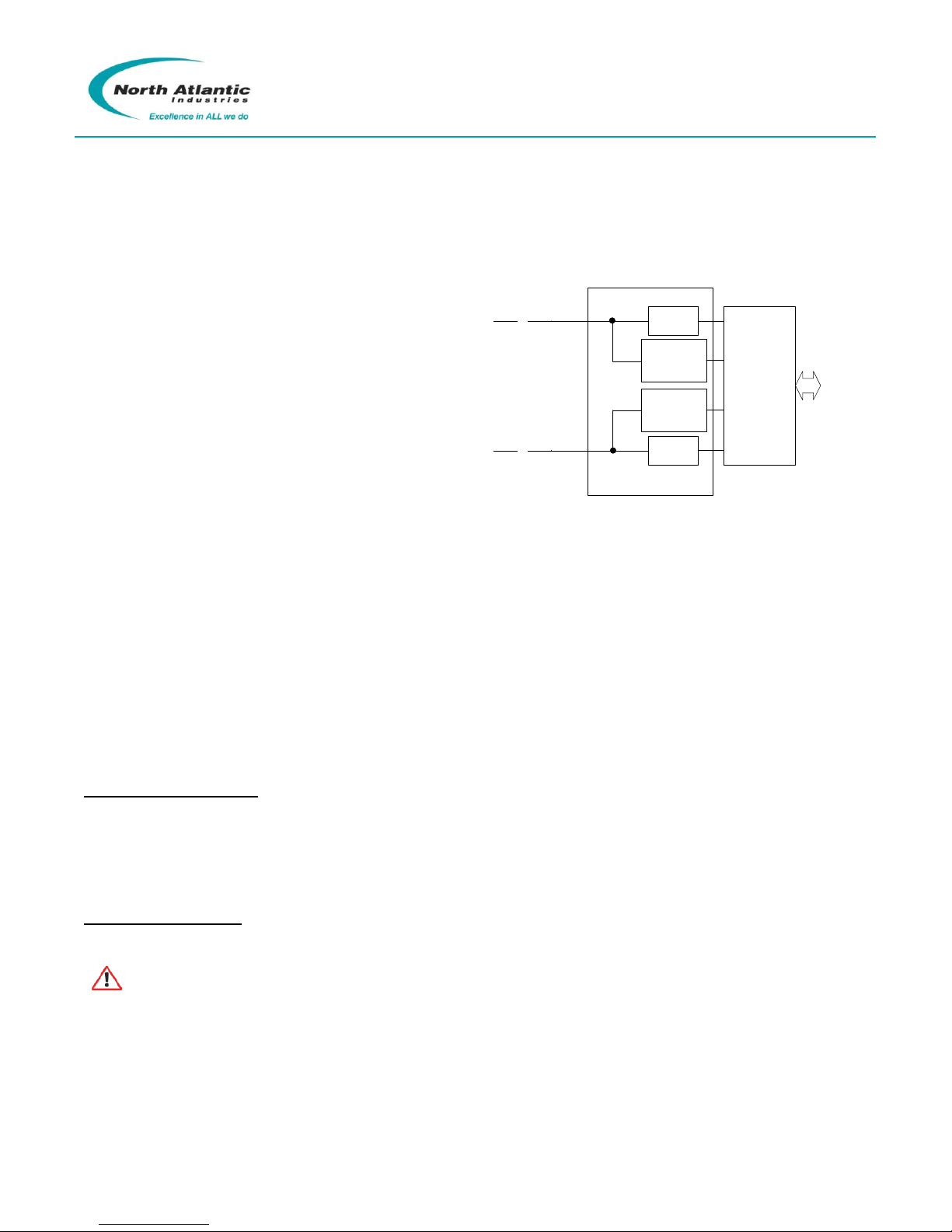
2
Wrap-Around
Test
S/D
DS 1
DS 2
State
Machine
DS Module Block Diagram
Module Bus
User Interface
Wrap-Around
Test
S/D
Signal and Reference
Isolation
1
D/S ONE/TWO CHANNEL (MODULES 1*, 2*, 3*, 4*)
(*See part number designation)
Principle of Operation
These new Digital-to-Synchro/Resolver (D/S)
modules are solid state designs that eliminate
the need for external transformers. Since these
modules operate down to 50 Hz, deleting the
previously large external transformers offers
huge space savings. The reduced size and
lower power consumption of these modules now
makes it possible to supply 10 channels on a 6U
card.
Two different modules are available within the
same package size: The first is a two-channel
1.5VA/2.2VA design that contains two separate
channels within one enclosure. The other is a
single channel 3.0VA design that will also drive
Torque Receivers. All outputs are short circuit
protected and the S2 (Z) leg can be grounded
without effecting performance. Any channel can be programmed for rotation (either continuous or with start/stop
angles). External amplifiers can be added to drive up to 30 VA with a frequency range of 50 to 400 Hz. Two-
speed (up to 1:255 ratio) outputs can be programmed (dual channel module). The processor will set a flag when it
senses that the maximum allowable misalignment of 90/gear ratio is exceeded.
New features in these modules now include a wrap capability for measuring each channel’s commanded output
angle and carrier frequency. The module’s extensive programmability now includes format selection (synchro or
resolver). A background calibration feature (pending), that is totally transparent to the operation of the channels,
constantly adjusts outputs for all load and environmental conditions. Each channel can be programmed for a
different output voltage, which can be programmed for either ratio-metric or absolute (fixed) output. Module power
ON/OFF capability provided for shutting down inactive channels.
Built-In Test (BIT) / Diagnostic Capability
Two different tests (one on-line and one off-line) can be selected:
The on-line (D2) Test initiates automatic background BIT testing that checks the output accuracy of each
channel by comparing the measured output angle to the commanded angle. Each channel is individually checked
to an accuracy of 0.2and each D/S Signal output and Reference input is continually monitored. User can
periodically clear to 00h and then read Test (D2) verification register again, after 0.1 seconds, to verify that
background bit testing is activated. Any failure triggers an Interrupt (if enabled) and the results are available in
Status Registers. The testing is totally transparent to the user, requires no external programming, has no effect on
the standard operation of the card, and can be enabled or disabled.
The off-line (D3) Test initiates a BIT test that generates and tests 24 different angles to a test accuracy of 0.2.
Results can be read from registers. External reference is required and outputs must be on. Any failure triggers an
Interrupt (if enabled). Testing requires no external programming, and can be initiated or stopped at any time.
CAUTION: Outputs must be ON and Reference supplied during this test and therefore active. Check
connected loads for possible interaction.

D/S One/Two Channel (Modules 1*, 2*, 3*, 4*)
75DS2 Operations Manual
North Atlantic Industries, Inc.
11/11/2011
Rev: 2011-11-11-1000
www.naii.com
Page 11 of 43
Wrap S/D Angle (Read)
The Wrap S/D Angle reads back the actual output signal (angle), which is used to verify that the actual output is
set to commanded angle. Read individual channels 1 or 2.
D15
D14
D13
D12
D11
D10
D9
D8
D7
D6
D5
D4
D3
D2
D1
D0
Wrap S/D Data () Hi
180
90
45
22.5
11.25
5.625
2.813
1.406
.703
.352
.176
.088
.044
.022
.011
.0055
Wrap S/D Data () Lo
.00274
.00137
.00068
.00034
.00017
.00008
.00004
.00002
X
X
X
X
X
X
X
X
Measured Reference Voltage
Each individual channel input signal voltage “VREF” is measured and the value reported to a corresponding read
register. The input voltage is reported to a resolution of 10 mv rms. The output is in integer decimal format. For
example, if channel 1 input REF voltage is 26.0 VRMS, the output measurement word from the corresponding
register would be 2600.
Measured Signal Voltage
Each individual channel input signal voltage “VL-L” is measured and the value reported to a corresponding read
register. The input voltage is reported to a resolution of 10 mv rms. The output is in integer decimal format. For
example, if channel 1 input signal voltage is 11.8 VRMS, the output measurement word from the corresponding
register would be 1180.
Signal Loss Threshold
Each individual channel input signal voltage “VL-L” is measured and the value reported to a corresponding read
register. The signal loss detection circuitry can be tailored to report a signal loss (at Signal Loss Status register) at
a user defined threshold. This threshold can be set to a resolution of 10 mv rms. Program the threshold by writing
the value of the voltage threshold in integer decimal format. For example, if channel 1 input signal loss voltage
threshold is to be 7 VRMS, the programmed word to the corresponding register would be 700 (2BCh).
Reference Loss Threshold
Each individual channel input reference voltage “VREF” is measured and the value reported to a corresponding
read register. The reference loss detection circuitry can be tailored to report a reference loss (at Reference Loss
Status register) at a user defined threshold. This threshold can be set to a resolution of 10 mv rms. Program the
threshold by writing the value of the voltage threshold in integer decimal format. For example, if channel 1 input
reference loss voltage threshold is to be 20 VRMS, the programmed word to the corresponding register would be
2000 (7D0h).
D/S Channel Frequency
Each individual channel Reference Frequency is measured and the value reported to a corresponding read
register. The input reference frequency is reported to a resolution of 1 Hz. The output is in integer decimal format.
For example, if channel 1 input excitation is 400 Hz, the output measurement word from the corresponding
register would be 400.

D/S One/Two Channel (Modules 1*, 2*, 3*, 4*)
75DS2 Operations Manual
North Atlantic Industries, Inc.
11/11/2011
Rev: 2011-11-11-1000
www.naii.com
Page 12 of 43
D/S Status, Signal Loss
Type: binary word
Range: N/A
Read/Write: R
Initialized Value: 0
Check the corresponding bit for a channel’s Signal Loss Status. A Signal input loss to that channel will trigger a
bit failure (=1) on a per channel basis; Passing status (=0). Signal Loss is indicated after 2 seconds. Signal input
monitoring is disabled during D3 or D0 Test. Any Signal Status failure, transient or intermittent, will latch the
Signal Status register. Reading any status bit will unlatch the entire register. Signal Status is part of background
testing and the status register may be checked or polled at any given time. When Status Interrupt is enabled,
Status Interrupt is reported through the Open Status Interrupt Vector in the General Use Memory Map.
REGISTER
D15
D14
D13
D12
D11
D10
D9
D8
D7
D6
D5
D4
D3
D2
D1
D0
FUNCTION
D/S Status, Signal Loss
X
X
X
X
X
X
X
X
X
X
X
X
X
X
Ch2
Ch1
CHANNEL STATUS BIT
D/S Wrap Select, Internal/External (Pending)
This register sets and determines where the wrap signal will be read from and will update in the Wrap S/D Angle
register. When set for internal, the wrap will be reading from the module output. When set for external, the wrap
will be reading from the external amplifier wrap input signals (See pin-out). “0” = internal wrap select, “1” =
external amplifier wrap select.
D15
D14
D13
D12
D11
D10
D9
D8
D7
D6
D5
D4
D3
D2
D1
D0
Wrap Select, Internal/External
X
X
X
X
X
X
X
X
X
X
X
X
X
X
CH2
CH1
D/S Status, External Amplifier (Pending)
This monitors the external amplifier BIT signal (See pin-out). Check the corresponding BIT status of the register
for each active channel that has the external amplifier enabled/connected. A “1” = BIT (OK), “0” = BIT (Fail)
D15
D14
D13
D12
D11
D10
D9
D8
D7
D6
D5
D4
D3
D2
D1
D0
Status, External Amplifier
X
X
X
X
X
X
X
X
X
X
X
X
X
X
CH2
CH1
D/S Write Angle –Single Speed
Write the desired commanded output angle. For single-speed applications (Ratio=1), write an “up to” 24-bit
integer (24-bit 2’s compliment integer) to the corresponding channel D/S Write Angle register. (ex. 330(in 16-bit
resolution) = EAABh written to Data Hi register only); 330(in 24-bit resolution) = EAAAAB –note that “EAAA” is
written to Data Hi register and “AB00” is written to Data Lo register).
WORD = (Angle (360/224)).
D15
D14
D13
D12
D11
D10
D9
D8
D7
D6
D5
D4
D3
D2
D1
D0
D/S Write Data () Hi
180
90
45
22.5
11.25
5.625
2.813
1.406
.703
.352
.176
.088
.044
.022
.011
.0055
D/S Write Data () Lo
.00274
.00137
.00068
.00034
.00017
.00008
.00004
.00002
X
X
X
X
X
X
X
X
Note: Writing to an Input Angle Register will stop any rotation initiated on that channel
D/S Write Angle –Two Speed
The dual channel module can automatically simulate two-speed applications (applies only to dual channel
modules). Write an “up to” 24-bit integer (24-bit 2’s compliment integer) to the corresponding channel D/S Write
Angle register to the coarse channel (channel 1). By entering a ratio in the D/S Ratio 1/2 register, the fine channel
(channel 2) will automatically output a signal proportional to the programmed coarse channel times the ratio
programmed.

D/S One/Two Channel (Modules 1*, 2*, 3*, 4*)
75DS2 Operations Manual
North Atlantic Industries, Inc.
11/11/2011
Rev: 2011-11-11-1000
www.naii.com
Page 13 of 43
D/S Rotation
Each channel may be configured for either start/stop or continuous rotation for applications that require it. In
start/stop mode, the user can program a rotational velocity and a stop angle. When triggered, either via a software
command or external pulse (selectable trigger mode), the output signal will start at the current position and
simulate rotation at the specified rotation rate and stop at the programmed stop angle. Re-initiating the trigger will
repeat the rotation. In continuous mode, the user will program a rotation rate and trigger the start of the rotation
either via software command or external trigger. Stopping rotation can be accomplished by either issuing a stop
rotation command or setting a commanded angle. Clockwise or counter-clockwise rotation is accomplished by
setting either a positive or negative 2’s complement word in the velocity register. Note: Writing to an Input Angle
Register will stop any rotation initiated on that channel.
D/S Stop Angle
May be used during implementation of D/S rotation. When the channel is set for start/stop rotation (D/S Rotation
Mode register), write the desired stop angle to this register. Write a 16-bit integer (or 16-bit 2’s compliment
integer) to the corresponding channel D/S Write Angle register. (ex. 330= EAABh).
WORD = (Angle (360/216)).
D/S Set Rotation Rate
May be used during implementation of D/S rotation. Write to the corresponding Set Rotation Rate registers (Hi
and Lo) a 2’s complement number representing the desired rotation rate, LSB = 0.015/sec.
Ex: 12 RPS = (12 x 360/0.015= 288000 = 46500h), -12 RPS = (-12 x 360/0.015= -288000 = 0xB9B00h)
Step size is 16 bits (0.0055) for up to 1.5 RPS, and then linearly decreases to 12 bits (0.088) at 13.6 RPS.
D/S Rotation Mode, Continuous or Start/Stop
For continuous rotation, set the corresponding channel bit to "0" in the Rotation Mode register. For rotation to
cease at a designated stop angle, set the bit to "1". For 2-speed applications, only the odd (coarse) channel
needs to be programmed (CH1).
D15
D14
D13
D12
D11
D10
D9
D8
D7
D6
D5
D4
D3
D2
D1
D0
D/S Rotation Mode
X
X
X
X
X
X
X
X
X
X
X
X
X
X
CH2
CH1
D/S Rotation Status
Check the corresponding bit of the D/S Rotation Status Register for condition of rotation (“Done”or “Not Done”)
for each channel. A ”1” means Rotation Done (output is static), “0” means Rotation Not Done (output is rotating)
on channel. Rotation monitoring is always enabled.
D15
D14
D13
D12
D11
D10
D9
D8
D7
D6
D5
D4
D3
D2
D1
D0
D/S Status, Rotation
X
X
X
X
X
X
X
X
X
X
X
X
X
X
CH2
CH1
Start Rotation
Implements a software command to initiate rotation (D/S Trigger Source Select Register is set for “internal”). First
set the Rotation Rate and Rotation Mode Registers for each channel that is to rotate. Then, to start rotation for the
corresponding channel, write a “1” to the corresponding channel D/S Start Rotation register.
Stop Rotation
To stop rotation for the corresponding channel, write a “1” to the corresponding channel D/S Stop Rotation
register. Channel will remain at the stopped angle until new input angles are set, or rotation is again initiated.
Note: An in-process rotation can also be stopped by commanding a new angle (D/S Write Angle).

D/S One/Two Channel (Modules 1*, 2*, 3*, 4*)
75DS2 Operations Manual
North Atlantic Industries, Inc.
11/11/2011
Rev: 2011-11-11-1000
www.naii.com
Page 14 of 43
D/S Set Reference Voltage
Utilized for setting input/output transformation ratio. Set the expected input reference voltage “VREF” to a
corresponding register. The input voltage is set with a resolution of 10 mv rms. The setting is in integer decimal
format. For example, if channel 1 expected input REF voltage is 26.0 VRMS, the set word to the corresponding
register would be 2600.
D/S Set Signal Voltage
Utilized for setting input/output transformation ratio. Set required output signal voltage “VL-L” to a corresponding
register. The output voltage is set with a resolution of 10 mv rms. The setting is in integer decimal format. For
example, if channel 1 Signal (VL-L) voltage is to be 11.8 VRMS, the set word to the corresponding register would
be 1180.
D/S BIT Test Enable
D15
D14
D13
D12
D11
D10
D9
D8
D7
D6
D5
D4
D3
D2
D1
D0
BIT Test Enable
X
X
X
X
X
X
X
X
X
X
X
X
D3
D2
X
X
Set bit to enable associated Built-In Self Test D2 or D3.
The on-line (D2) Test - Writing “1” to the D2 bit of the D/S Test Enable Register initiates status reporting of the
automatic background BIT testing that checks the output accuracy of each channel by comparing the measured
output angle to the commanded angle. The status bits will be set to indicate an accuracy (0.2º) problem and the
results can be read from D/S Status registers within 2 seconds and if enabled, an interrupt will be generated (See
Interrupt Register). Writing a “0” deactivates the status reporting. The testing is totally transparent to the user,
requires no external programming, and has no effect on the standard operation of this card. Note: Outputs must
be ON and Reference supplied for test to function. Card will write 55h (every 0.1 seconds) to the D/S Test
(D2) Verify register when D2 is enabled. User can periodically clear to 00h and then read the D/S Test (D2)
Verify register again, after 0.1 seconds, to verify that BIT Testing is activated. This test continuously sequences
between the channels on the card with each output being measured for approximately 180mSec. If the measured
angle has an error greater the 0.2º, a flag will be set in the appropriate register. If the input angle is stepped more
then 0.2º during a test cycle, the test cycle will not generally indicate an error. In addition, each D/S Reference
input and signal output is continually monitored. Any failure triggers an Interrupt (if enabled) and the results are
available in the D/S Signal and D/S Reference Status registers.
The off-line (D3) Test - Writing “1” to the D3 bit of the D/S Test Enable Register initiates a BIT Test that
generates and tests 24 different angles to an accuracy of 0.2. External reference is required and outputs must be
ON. The D/S Status bits will be set to indicate an accuracy problem. Results are available in the D/S Test Status
registers and if enabled, an interrupt will be generated (See Vector Interrupt Registers). Test cycle takes about 30
seconds and the D3 bit changes from “1” to “0” when test is complete. The testing requires no external
programming, and can be terminated at any time by writing a “0” to the D3 bit of the D/S BIT Test Enable register.
CAUTION: Outputs must be ON and Reference must be supplied during this test. The outputs are
therefore active. Check connected loads for possible interaction.

D/S One/Two Channel (Modules 1*, 2*, 3*, 4*)
75DS2 Operations Manual
North Atlantic Industries, Inc.
11/11/2011
Rev: 2011-11-11-1000
www.naii.com
Page 15 of 43
D/S Status, BIT Test
Check the corresponding bit of the D/S BIT Test Status Register for status of BIT (Test-Accuracy) Testing for
each “active”channel. A ”1” means Accuracy Failed; “0” means Accuracy OK. Channels that are “inactive”are
also set to “0”. The status bits will be set to indicate an accuracy (0.2º) problem and the results can be read from
D/S Status Registers within 2 seconds and, if enabled, an interrupt will be generated (See Interrupt Register).
This test continuously sequences between the channels on the card with each output being measured for
approximately 180mSec. If the measured angle has an error greater the 0.2º, a flag will be set in the appropriate
register. If the input angle is stepped more than 0.2º during a test cycle, the test cycle will not generally indicate
an error.
D/S channels, by default, are set for monitoring the channel background BIT (Built-In-Test) status reporting; “ON”
or “ACTIVE”. The front panel BIT LED illuminates (Red) if any channel reports a BIT fault. For BIT status to work
properly on an “active” channel, the D/S channel must have a valid Reference source applied and the D/S
channel power set to “ON” (so there is a valid signal being generated). If channels are not being used, it is
recommended that the channel BIT status report be turned off (or set INACTIVE). However, it should be noted
that the channel BIT status register latches the contents of a failure until read. Simply setting the channel
“INACTIVE” will not clear the BIT status register or extinguish the front panel BIT fault LED if a fault was
previously detected.
The D/S BIT Test Status register should be queried (read) to insure the register is unlatched which will enable the
BIT status register to be re-written during next status update (which, when the channel is set INACTIVE, should
clear the fault). Once this is done, the front panel BIT LED will extinguish –as long as the channels that are active
are working properly and the channels not being utilized are set INACTIVE.
Note: When D/S Wrap Select External/Internal register is set for “external”, the BIT wrap will be read from the
external amplifier wrap input signals (See pin-out). Also, the BIT tolerance will be adjusted for the amplifier
accuracy specification.
D15
D14
D13
D12
D11
D10
D9
D8
D7
D6
D5
D4
D3
D2
D1
D0
D/S Status, BIT Test
X
X
X
X
X
X
X
X
X
X
X
X
X
X
CH2
CH1
Test (D2) Verify
Card will write 55h at Test (D2) Verify register when (D2) is enabled, approximately every (1) second. User can
clear to 00h and then read again, after approximately (1) second, to verify that background bit testing is activated.
D/S Ratio 1/2
Utilized for automatically simulating dual speed synchro/resolver. Only applies to dual channel module. Set
desired ratio between coarse (channel 1) and fine (channel 2) channels. Enter the desired ratio, as an integer
number, in the D/S Ratio 1/2 register corresponding to the pair of channels to be used as a two-speed channel.
Example: Single speed = 1; 36:1 = integer 36. (Ratio range from 1 to 255). By entering a ratio in the D/S Ratio
1/2 register, the fine channel (channel 2) will automatically output a signal proportional to the programmed coarse
channel times the ratio programmed.
D/S Output Mode
The D/S Output Mode register is utilized for selecting either ratio-metric or absolute (fixed) mode voltages. Ratio-
metric Mode, when selected, will cause the output signal voltage of the channel to vary with the input Reference
Voltage. Fixed Mode, when selected, will cause the output signal voltage of the channel NOT to vary with the
input Reference Voltage. Set corresponding channel bit to “0” for Ratio-metric Mode. Set corresponding channel
bit to “1” for Fixed Mode.
D15
D14
D13
D12
D11
D10
D9
D8
D7
D6
D5
D4
D3
D2
D1
D0
D/S Output Mode
X
X
X
X
X
X
X
X
X
X
X
X
X
X
CH2
CH1
D/S One/Two Channel (Modules 1*, 2*, 3*, 4*)
75DS2 Operations Manual
North Atlantic Industries, Inc.
11/11/2011
Rev: 2011-11-11-1000
www.naii.com
Page 16 of 43
D/S Synchro / Resolver Select
As required, write a “11” or “00” (Synchro = 11; Resolver = 00) to each corresponding channel bit pair,
representing a channel commanded output format, of the Synchro/Resolver register.
D15
D14
D13
D12
D11
D10
D9
D8
D7
D6
D5
D4
CH2
D2
CH1
D0
D/S Synchro / Resolver Select
X
X
X
X
X
X
X
X
X
X
X
X
D3
D2
D1
D0
D/S Torque Receiver Select
When selected, channel will be subjected to an automatic control algorithm which minimizes torque receiver
power draw. Applies only to the single channel modules. Normal = “0”; Torque Receiver = “1”
D15
D14
D13
D12
D11
D10
D9
D8
D7
D6
D5
D4
D3
D2
D1
D0
D/S Torque Receiver Select
X
X
X
X
X
X
X
X
X
X
X
X
X
X
X
CH1
D/S Trigger Source Select
May be used during implementation of D/S rotation. When triggered, the D/S channel will commence rotation.
Triggering may be initiated via “internal” software command (D/S Start Rotation register) or via “external’ signal
application (see pin-out). Internal = “0x29”; External = “0x28”
D15
D14
D13
D12
D11
D10
D9
D8
D7
D6
D5
D4
D3
D2
D1
D0
Trigger Source Select
X
X
X
X
X
X
X
X
X
X
D
X
D
X
X
D
D/S Trigger Slope Select
May be used during implementation of D/S rotation when D/S Trigger Source Select register is set for “external”.
For rotation trigger on positive slope, set the corresponding channel bit to "0" in the Trigger Slope Select register.
For negative slope, set the bit to "1"
D15
D14
D13
D12
D11
D10
D9
D8
D7
D6
D5
D4
D3
D2
D1
D0
Trigger Slope Select
X
X
X
X
X
X
X
X
X
X
X
X
X
X
CH2
CH1
D/S Module Power Enable
The D/S Module Power Enable register is utilized for module channel output/power control. Set the bit,
corresponding to either channel, to enable the power output stage of the D/S channel(s). “1” = Enable; “0” =
Disabled. For dual channel modules, writing a “1” to either or both channel bits will enable and turn the output
stage power “on”. To disable, or turn off power to the output stage, all channels (both) bits must be set to “0”.
Initialized default is “00”.
D15
D14
D13
D12
D11
D10
D9
D8
D7
D6
D5
D4
D3
D2
D1
D0
D/S Module Power Enable
X
X
X
X
X
X
X
X
X
X
X
X
X
X
CH2
CH1
D/S Output Enable
NOTE: Single Channel D/S Only
Set the corresponding bit to “1” in the Output On/Off Register. To turn OFF channel, set corresponding bit to “0”.
Default: Set to OFF. (OFF = “0”; ON = “1”)
D15
D14
D13
D12
D11
D10
D9
D8
D7
D6
D5
D4
D3
D2
D1
D0
Trigger Source Select
X
X
X
X
X
X
X
X
X
X
X
X
X
X
X
CH1
D/S One/Two Channel (Modules 1*, 2*, 3*, 4*)
75DS2 Operations Manual
North Atlantic Industries, Inc.
11/11/2011
Rev: 2011-11-11-1000
www.naii.com
Page 17 of 43
D/S Active Channel Select
Allows the BIT Test Status register to be updated. For BIT status to work properly on an “active” channel, the D/S
channel must have a valid Reference source applied and the D/S channel power set to “ON” (so there is a valid
signal being generated). If channels are not being used, it is recommended that the channel BIT status report be
turned off (or set “Inactive”). Set the bit, corresponding to each channel to be monitored during BIT testing, in the
Active Channel Register for the particular D/S channel. “1” = Active; “0” = not used.
Note: Omitting this step will produce false alarms because unused channels will set faults.
D15
D14
D13
D12
D11
D10
D9
D8
D7
D6
D5
D4
D3
D2
D1
D0
D/S Active Channel Select
X
X
X
X
X
X
X
X
X
X
X
X
X
X
CH2
CH1
D/S Status, Reference Loss
Check the corresponding bit of the D/S Reference Status register for condition of the reference input for each
active channel. A ”1” means Reference has been lost, “0” means Reference is okay on active channels (D/S
Active Channel Select register). Channels that are inactive are also set to “0”. Reference loss is detected within 2
seconds. Reference monitoring is always enabled. Any D/S reference loss detection, transient or intermittent, will
latch the D/S Reference Status register. Reading will unlatch the register.
D15
D14
D13
D12
D11
D10
D9
D8
D7
D6
D5
D4
D3
D2
D1
D0
D/S Status, Reference Loss
X
X
X
X
X
X
X
X
X
X
X
X
X
X
CH2
CH1
D/S Status, Phase Lock Loss
Check the corresponding bit of the D/S Phase Lock Loss Register for condition of the phase lock between the
reference input and signal output for each active channel. A ”1” means Phase Lock Loss has occurred, “0”
means Phase Lock okay on active channels(D/S Active Channel Select Register). Channels that are inactive are
also set to “0”. (Phase Lock loss is detected within 2 seconds). Phase Lock monitoring is always enabled. Any
D/S Phase Lock Loss status failure, transient or intermittent, will latch the D/S Phase Lock Loss Status Register.
Reading will unlatch register.
D15
D14
D13
D12
D11
D10
D9
D8
D7
D6
D5
D4
D3
D2
D1
D0
D/S Status, Phase Lock Loss
X
X
X
X
X
X
X
X
X
X
X
X
X
X
CH2
CH1
D/S Set Phase Offset
The phase of each individual channel signal may be offset from the Reference signal. The phase may be adjusted
at a resolution of 0.1 deg / bit. Program the desired lead or lag in integer as a 2’s complement word format. For
example, if channel 1 output signal is to lead the reference signal by 1.6 degrees, program the corresponding
channel phase register to 16 (10h). If channel 1 output signal is to lag the reference signal by 1.6 degrees,
program the corresponding channel phase register to -16 (FFF0h). Phase shift range is -90 <= x <= 90.
Reference Loss Interrupt Enable
Set the bit to enable interrupts for the corresponding channel. When enabled, a reference input loss (D/S Status,
Reference) will trigger an interrupt. Default is “0” to disable interrupt on all channels. When Status Interrupt is
enabled, Status Interrupt is reported through the Reference Loss Interrupt Vector.
D15
D14
D13
D12
D11
D10
D9
D8
D7
D6
D5
D4
D3
D2
D1
D0
Reference Loss Interrupt Enable
X
X
X
X
X
X
X
X
X
X
X
X
X
X
CH2
CH1
D/S One/Two Channel (Modules 1*, 2*, 3*, 4*)
75DS2 Operations Manual
North Atlantic Industries, Inc.
11/11/2011
Rev: 2011-11-11-1000
www.naii.com
Page 18 of 43
Signal Loss Interrupt Enable
Set the bit to enable interrupts for the corresponding channel. When enabled, a signal input loss (D/S Status,
Signal Loss) will trigger an interrupt. Default is “0” to disable interrupt on all channels. When Status Interrupt is
enabled, Status Interrupt is reported through the Signal Loss Interrupt Vector.
D15
D14
D13
D12
D11
D10
D9
D8
D7
D6
D5
D4
D3
D2
D1
D0
Signal Loss Interrupt Enable
X
X
X
X
X
X
X
X
X
X
X
X
X
X
CH2
CH1
BIT Test Fail Interrupt Enable
Set the bit to enable interrupts for the corresponding channel. When enabled, a BIT Test Failure (D/S Status, BIT
Test) will trigger an interrupt. Default is “0” to disable interrupt on all channels. When Status Interrupt is enabled,
Status Interrupt is reported through the BIT Test Loss Interrupt Vector.
D15
D14
D13
D12
D11
D10
D9
D8
D7
D6
D5
D4
D3
D2
D1
D0
BIT Test Fail Interrupt Enable
X
X
X
X
X
X
X
X
X
X
X
X
X
X
CH2
CH1
Phase Lock Loss Interrupt Enable
Set the bit to enable interrupts for the corresponding channel. When enabled, a Phase Lock Loss (D/S Status,
Phase Lock Loss) will trigger an interrupt. Default is “0” to disable interrupt on all channels. When Status Interrupt
is enabled, Status Interrupt is reported through the Phase Lock Loss Interrupt Vector.
-
D15
D14
D13
D12
D11
D10
D9
D8
D7
D6
D5
D4
D3
D2
D1
D0
Phase Lock Loss Interrupt Enable
X
X
X
X
X
X
X
X
X
X
X
X
X
X
CH2
CH1
OSC (Optional Onboard Reference Supply) Set Frequency
Type: 16-bit unsigned integer
Range: 47 to 10,000 Hz
Read/Write: R/W
Initialized Value: N/A
Program Reference Frequency, where LSB is 0.01 Hz. For example: To program 400 Hz, 400 x 100= 40,000,
which equals 0x9C40. In this example, 0x0000 would be programmed in the Reference Frequency High register,
and 0x9C40 would be programmed in the Reference Frequency Low register. To program 10,000 Hz, 10,000 x
100= 1,000,000, which equals 0xF4240. In this example, 0x000F would be programmed in the Reference
Frequency High register, and 0x4240 would be programmed in the Reference Frequency Low register.
REGISTER
D15
D14
D13
D12
D11
D10
D9
D8
D7
D6
D5
D4
D3
D2
D1
D0
FUNCTION
327.68
163.84
81.92
40.96
20.48
10.24
5.12
2.56
1.28
0.64
0.32
0.16
0.08
0.04
0.02
0.01
approximate value
REF FREQUENCY LO
D
D
D
D
D
D
D
D
D
D
D
D
D
D
D
D
D=DATA BIT (Hz)
REGISTER
D15
D14
D13
D12
D11
D10
D9
D8
D7
D6
D5
D4
D3
D2
D1
D0
FUNCTION
0
0
0
0
0
0
0
0
0
0
0
0
5242.88
2621.44
1310.72
655.36
approximate value
REF FREQUENCY HI
D
D
D
D
D
D
D
D
D
D
D
D
D
D
D
D
D=DATA BIT (Hz)
D/S One/Two Channel (Modules 1*, 2*, 3*, 4*)
75DS2 Operations Manual
North Atlantic Industries, Inc.
11/11/2011
Rev: 2011-11-11-1000
www.naii.com
Page 19 of 43
OSC (Optional Onboard Reference Supply) Set Voltage
Type: 16-bit unsigned integer
Range: 2.0 to 28.0 Vrms, or 115 Vrms
Read/Write: R/W
Initialized Value: N/A
Program Reference Voltage, where LSB is 0.01 Vrms. For example: To program 26.1 Vrms, 26.1 x 100= 2610,
which equals 0xA32. In this example, 0x0000 would be programmed in the Reference Voltage High register, and
0x0xA32 would be programmed in the Reference Voltage Low register. To program 115 Vrms, 115 x 100=
11,500, which equals 0x2CEC. In this example, 0x0000 would be programmed in the Reference Voltage High
register, and 0x2CEC would be programmed in the Reference Voltage Low register. Note: Reference Voltage
High register always remains at 0x0000.
REGISTER
D15
D14
D13
D12
D11
D10
D9
D8
D7
D6
D5
D4
D3
D2
D1
D0
FUNCTION
0
0
81.92
40.96
20.48
10.24
5.12
2.56
1.28
0.64
0.32
0.16
0.08
0.04
0.02
0.01
approximate value
REF FREQUENCY LO
D
D
D
D
D
D
D
D
D
D
D
D
D
D
D
D
D=DATA BIT (Hz)
REGISTER
D15
D14
D13
D12
D11
D10
D9
D8
D7
D6
D5
D4
D3
D2
D1
D0
FUNCTION
0
0
0
0
0
0
0
0
0
0
0
0
0
0
0
0
approximate value
REF FREQUENCY HI
D
D
D
D
D
D
D
D
D
D
D
D
D
D
D
D
D=DATA BIT (Hz)
Interrupt Vector
The Interrupt Vector Registers store the vectors for the specific interrupts generated by the module which are
used for failure reports. If the same vector is loaded into each register, the same interrupt routine will be invoked
by all interrupts. If unique vectors are loaded into the registers, a different Interrupt Service Routine (ISR) can be
invoked by each interrupt. Write 16-bit integer (0-255).
The Signal Loss interrupt vector will be serviced when the Signal Loss status is set and the interrupt has been
enabled.
The Reference Loss interrupt vector will be serviced when the Reference Loss status is set and the interrupt
has been enabled.
The BIT interrupt vector will be serviced when the Bit (failure) status is set and the interrupt has been
enabled.
The Lock Loss interrupt vector will be serviced when the Lock Loss status is set and the interrupt has been
enabled.
D/S (1*, 2*, 3*, 4*) (PCI) MODULE MEMORY MAP
75DS2 Operations Manual
North Atlantic Industries, Inc.
11/11/2011
Rev: 2011-11-11-1000
www.naii.com
Page 20 of 43
D/S (1*, 2*, 3*, 4*) (PCI) MODULE MEMORY MAP
000
Wrap S/D Angle Lo CH1
R
140
D/S Set Reference Volt Lo CH1
W/R
1E8
D/S Set Phase Offset CH1
W/R
004
Wrap S/D Angle Hi CH1
R
144
D/S Set Reference Volt Hi CH1
W/R
1EC
D/S Set Phase Offset CH2
W/R
008
Wrap S/D Angle Lo CH2
R
148
D/S Set Reference Volt Lo CH2
W/R
1F4
D/S Rotation Status CH1/2
R
00C
Wrap S/D Angle Hi CH2
R
14C
D/S Set Reference Volt Hi CH2
W/R
330
OSC Set Voltage Lo
W/R
064
Measured Reference Voltage CH1
R
160
D/S Set Signal Volt Lo CH1
W/R
334
OSC Set Voltage HI
W/R
068
Measured Reference Voltage CH2
R
164
D/S Set Signal Volt Hi CH1
W/R
338
OSC Set Frequency Lo
W/R
070
Measured Signal Voltage CH1
R
168
D/S Set Signal Volt Lo CH2
W/R
33C
OSC Set Frequency Hi
W/R
074
Measured Signal Voltage CH2
R
16C
D/S Set Signal Volt Hi CH2
W/R
3A0
Start Rotation CH1
W
080
Signal Loss Threshold CH1
W/R
178
D/S Status, External Amplifier
R
3A4
Start Rotation CH2
W
084
Signal Loss Threshold CH2
W/R
17C
D/S Wrap Select, Internal/External
W/R
3B0
Stop Rotation CH1
W
08C
Reference Loss Threshold CH1
W/R
3B4
Stop Rotation CH2
W
090
Reference Loss Threshold CH2
W/R
180
D/S BIT Test Enable
W/R
184
D/S Ratio 1/2
W/R
700
D/S Status, BIT Test
R
098
Channel 1 Frequency
R
188
D2 Test Verify
W/R
704
Reference Loss Interrupt Enable
W/R
09C
Channel 2 Frequency
R
18C
D/S Output Mode
W/R
708
Signal Loss Interrupt Enable
W/R
0B0
Status, Signal Loss
R
190
D/S Rotation Mode
W/R
70C
BIT FAIL Interrupt Enable
W/R
198
D/S Synchro/Resolver Select
W/R
710
Phase Lock Loss Interrupt Enable
W/R
0C0
D/S Write Angle Lo CH1
W/R
19C
D/S Torque Receiver Select
W/R
0C4
D/S Write Angle Hi CH1
W/R
768
Module Design Version
R
0C8
D/S Write Angle Lo CH2
W/R
1A0
D/S Trigger Source Select CH1
W/R
76C
Module Design Revision
R
0CC
D/S Write Angle Hi CH2
W/R
1A4
D/S Trigger Source Select CH2
W/R
770
Module DSP Revision
R
0E4
D/S Stop Angle CH1
W/R
1AC
D/S Trigger Slope Select
W/R
774
Module FPGA Revision
R
0E8
D/S Stop Angle CH2
W/R
1B0
D/S Output Enable (1 CH only)
W/R
778
Module ID Revision
R
100
D/S Set Rotation Rate Lo CH1
W/R
1C0
D/S Module Power Enable
W/R
7C0
Vector Interrupt BIT Fail
W/R
104
D/S Set Rotation Rate Hi CH1
W/R
1C8
D/S Active Channel Select
W/R
7C4
Vector Interrupt REF Loss
W/R
108
D/S Set Rotation Rate Lo CH2
W/R
1CC
D/S Status, Reference Loss
R
7C8
Vector Interrupt Signal Loss
W/R
10C
D/S Set Rotation Rate Hi CH2
W/R
1D0
D/S Status, Phase Lock Loss CH1/2
R
7CC
Vector Interrupt Phase Lock Loss
W/R
Table of contents
Popular Media Converter manuals by other brands


Sinclair Audio
Sinclair Audio ProloguE 100 manual

CYP
CYP CDPS-US100R Operation manual

Sun Microsystems
Sun Microsystems SunSwift SPARCserver 1000 user manual

Contemporary Research
Contemporary Research ICE-HE product manual

Cobalt Digital Inc
Cobalt Digital Inc BBG-1090-DEC-MPEG product manual

AxelTech
AxelTech EX2-2200 user manual


