Nova Electronics MC8022P User manual

PCI Bus
2/4-Axis Motor Control Board
MC8022P/MC8042P
Hardware Manual
2013-04-17 Ver. 1.0
NOVA electronics
NOVA electronics MC8022P/MC8042P - i
Prevent Electrostatic Discharge
ATTENTION: MC8022P/MC8042P is sensitive to electrostatic discharge, which can
cause internal damage and affect normal operation. Follow these guidelines when
you handle MC8022P/MC8042P:
・Touch a grounded object to discharge potential static.
・Wear an approved grounding wrist strap.
・Hold both ends of the board between your fingers or hold a mounting bracket.
・Do not touch connectors or pins on component boards.
・Do not touch circuit components on MC8022P/MC8042P.
・Store MC8022P/MC8042P in appropriate static-safe packaging when not in use.
Safety Notice
WARNING: MC8022P/ MC8042P is not designed or intended to be fail-safe, or for
use in any application requiring fail-safe performance, such as in life-support or
safety devices or systems that could lead to death, personal injury or severe
property or environmental damage (individually and collectively, "critical
applications"). Customer must be fully responsible for the use of MC8022P/MC8042P
in critical applications. Provide adequate design and operating safeguards in order to
minimize risks associated with customer's applications when incorporating
MC8022P/MC8042P in a system.
Before you begin
ATTENTION: Before using MC8022P/MC8042P, read this manual thoroughly to
ensure correct usage and observe all the instructions given in this manual.
Checking the Contents
ATTENTION: When you unpack a package of MC8022P/MC8042P, check for the
following accessories. If something is missing or broken, contact the place of
purchase.
MC8042P or MC80222P 1
I/O Cable (CN2) 1
The user’s manual and software are not with the package for resource-saving. If you
need additional manuals or software, contact the place of purchase or contact us
to the following email address as "novaelec_info@novaelec.co.jp".
- i -
NOVA electronics MC8022P/MC8042P - ii
Consulting Other Manuals
ATTENTION: The circuit of MC8022P/MC8042P consists of mainly 4-axis motion
control IC “MCX304”, a PCI-bus interface circuit and I/O interface circuits of each
axis. Basic functions of this board all depend on MCX304, so please refer to the
user’s manual of MCX304 regarding these functions. This manual describes about
Electric Specification of each axis I/O signal. Regarding the installation on Windows,
API function for board control and sample program files for this board, see “MC8000P
Device Driver Manual.”
Environmental Conditions
ATTENTION: Use the following environmental conditions.
Operating Temperature 0~45°C(32~113°F)
Humidity 20~90% (no condensation)
Floating dust Not to be excessive
Corrosive gases None
Electric supply source DC+5V (±5%), external source: DC+24V
Inspection and Maintenance
ATTENTION: Perform inspection and maintenance periodically for correct use.
Cable connection
T
he connector of the board and a cable should
properly be connected.
Card-edge No dust and no corrosion.
Connector terminal area No dust and no corrosion.
On the IC and board No excessive dust and no foreign substance.
Handling Precautions
ATTENTION:
・Do not use in any location subject to shock, vibration, magnetism and electricity.
Otherwise, the equipment may be damaged or malfunctioned.
・Do not disassemble, repair or modify the equipment.
・Do not connect or disconnect the board or cables while power is applied.
Otherwise
,
breakdown or o
p
eration error ma
y
result.
・Information in this manual is subject to change without notice.
・Windows are registered trademark of Microsoft Corporation.
- ii -

NOVA electronics MC8022P/MC8042P - iii
1.Outline ................................................................... 1
1.1 MCX304 Functional Restriction ...................................................................................................... 2
1.2 PCI Bus Interface ........................................................................................................................... 2
1.3 Each Axis I/O Interface................................................................................................................... 2
2.I/O Address Setting and Register .......................... 3
3.I/O Signals ............................................................. 4
3.1 CN2 Connector (Rear connector)................................................................................................... 4
3.2 CN3, 4 Connector (Connector on the board).................................................................................. 6
3.3 Drive Pulse Output Signal (nP+P, nP+N, nP-P, nP-N) .................................................................... 8
3.4 General Output Signal and Deviation Counter Clear Output Signal (OUT1~14, nOUT0/DCC) ...... 8
3.5 Over Run Limit Input Signal (nLMT+, nLMT-)............................................................................... 10
3.8 Input Signals for Servo Motor (nINPOS, nALARM) ...................................................................... 13
3.10 Driving by External Signal (nEXOP+, nEXOP-) ............................................................................ 15
3.11 Emergency Stop Input Signal (EMG)............................................................................................ 15
3.12 External Power (VEX) .................................................................................................................. 15
4.Interrupt ............................................................... 16
5.Connection Example for Motor Driver.................. 17
5.1 Connection Example for Stepper Motor Driver ............................................................................. 17
5.2 Connection Example for AC servo motor driver............................................................................ 18
6.Input/Output Signals Timing................................. 19
6.1 Reset............................................................................................................................................ 19
6.2 Beginning of Driving ..................................................................................................................... 19
6.3 Input Pulse Timing........................................................................................................................ 19
6.4 Instant Stop Timing....................................................................................................................... 20
6.5 Decelerating Stop Timing ............................................................................................................. 20
7.Board Dimensions ............................................... 21
8.Specifications ...................................................... 22
- iii -
NOVA electronics MC8022P/MC8042P - 1
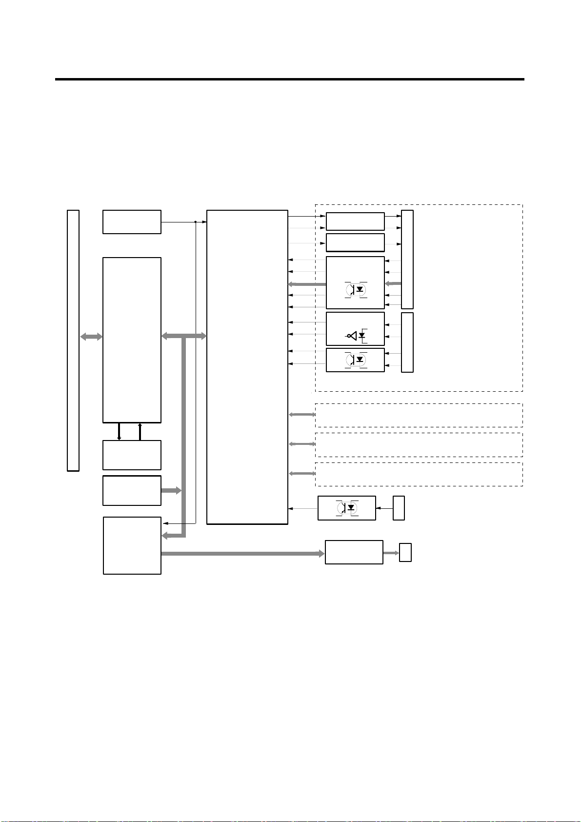
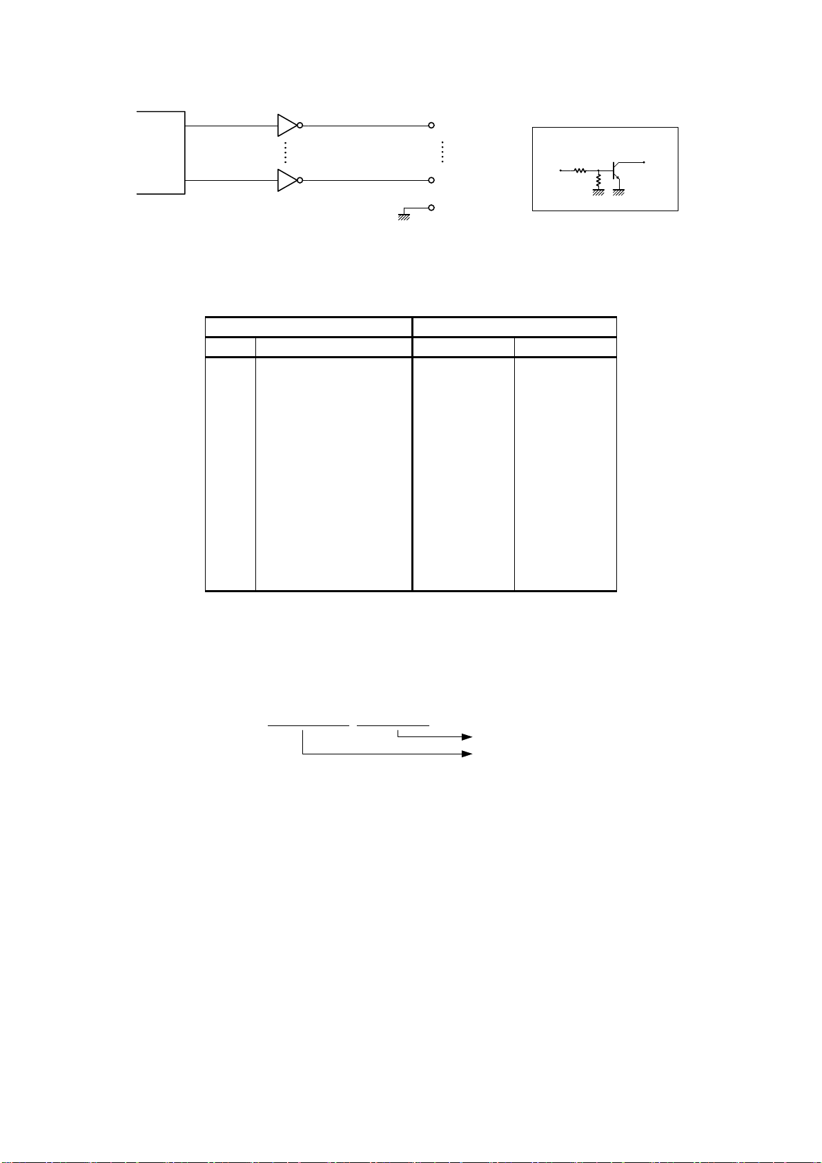
1. Outline
MC8022P/MC8042P is a PCI-bus compliant circuit board equipped with 4-axis motion control IC “MCX304”. It can
independently control 2/4-axis of either stepper motor or pulse type servo drives for position and speed controls.
MC8022P/MC8042P functional block diagram is shown as follows. MC8022P/MC8042P consists of mainly 4-axis motion
control IC “MCX304”, a PCI-bus interface circuit and I/O interface circuits of each axis: X, Y, Z and U. Therefore, basic
functions of this board all depend on MCX304, so please refer to the user’s manual of MCX304 regarding these functions.
MCX304
Line Driver
AM26C31
Output Buffer
TD62503
XP+P/N +direction pulse output
XP- P/N - direction pulse output
XOUT0/DCC general output
Photo Coupler
XLMT+ +direction limit
XLMT- -direction limit
XSTOP2~0 deceleration/
XINPOS servo in- position
XALARM servo alarm
High- speed
XECAP/N encoder A- phase
XECBP/N encoder B- phase
X axis I/O Interface
Y axis I/O Interface
Z axis I/O Interface
U axis I/O Interface
(same as X axis)
(same as X axis) *Only for MC8042P
(same as X axis) *Only for MC8042P
XPP
XPM
XLMTP
XLMTM
XSTOP2~0
XINPOS
XALARM
XECA
XECB
Crystal Oscillator
16MHz CLK
EMG emergency stop for all axes
XEXOP+ +direction driving
XEXOP- - direction driving
XEXPP
XEXPM
EMGN
EEPROM
93LC66
APIC21
PCI Interface
Adapter
1 point/deviation C clear
PIX132
For multiple
Address SW
CN1
PCI Bus
Note: Input signals need an external electric supply 24V.
XOUT0/DCC
CN2CN3
CN2
CN2: PC rear connector
CN1: PCI card edge connector
CN3, 4: Connectors on the board
Photo Coupler IC
instant stop
General Purpose
Input/Output IC
CLK
Output Buffer
TD62503
CN4
OUT1~14 general output
14 points
MC8022P/MC8042P Circuit Block Diagram
- 1 -

NOVA electronics MC8022P/MC8042P - 2
1.1 MCX304 Functional Restriction
MC8022P/MC8042P does not support the following MCX304 general output signals. However, it is equipped with
PIX132(NOVA Electronics) on the board, so that it has fourteen general output signals and nOUT general output signals of
MCX304.
MCX304-nOUT1 output signal
nSTOP2/OUT1 pin of MCX304 is used as STOP2 input, so it cannot be used as general output nOUT1.
MCX304-nOUT2, 3 output signals
D15~D8 are used due to 16-bit data bus performance. Therefore, it cannot be used as nOUT2, 3 signals.
1.2 PCI Bus Interface
■ Occupied I/O Address
The board requires 24 I/O address locations for PCI bus. I/O addressing is determined by “plug and play” function of Windows.
■ Data Length
Data length is 16-bit. Read/Write access cannot be performed per byte.
■ Interrupt Signal
When using an interrupt to PCI bus, the board uses IRQ determined by “plug and play” function of Windows.
1.3 Each Axis I/O Interface
■ Drive Pulse Output (nP+P/N, nP-P/N)
Drive pulses in the +/- direction for motor driving are output a 50% duty cycle of from 1PPS to 4MPPS.
Drive pulse output signals of each direction are the differential line-driver output of AM26C31 line driver or equivalent.
■ General Output (OUT1~14, nOUT0)
General output signals (14points) from PIX132, output buffer uses TD62503 (Toshiba) and is the open collector output with
sustaining voltage 35V. These signals are placed in the connector CN4 on the board. nOUT0 signal for each axis can be used as a
deviation counter clear signal (DCC) for a servomotor in automatic home search executing. nOUT0 signal is placed in the rear
connector CN2.
■ Over Run Limit Input (nLMT+, nLMT-)
Input signal to disable output pulse for + and – direction respectively. Decelerating stop and instant stop for active can be
selected in mode setting. These input signals are isolated by photo coupler from internal circuit. external 24V power supply is
needed.
■ Decelerating Stop/Instant Stop Input (nSTOP2~0)
In automatic home search, this input signal is to stop drive pulse in deceleration or immediately from outside. Enable/Disable
and active logical level can be selected in mode setting and each axis has three inputs. For encoder Z-phase signal, input to
nSTOP2. The user can connect to the driver whose type of output circuit is open collector or differential line-driver. These input
signals are isolated by photo coupler from internal circuit.
■ Servo Motor Input (nINPOS, nALARM)
INPOS (in-position) signal and ALARM signal for servo motor drivers can be input, which can also be used as general input
signals. These input signals are isolated by photo coupler from internal circuit.
■ Encoder Input (nECAP/N, nECBP/N)
This signal inputs A/B phase signal from an encoder, which is placed in the connector CN3 on the board. nECAP/N, nECBP/N
signals are for an encoder A/B phase signal input and count up or down 32-bit real position counter inside MCX304. These input
signals are isolated by photo coupler from internal circuit and can easily be connected to a differential output line-driver.
■ Driving by External Input(nEXOP+, nEXOP-)
This signal externally controls driving in the + or – direction, which is placed in the connector CN3 on the board. In fixed
driving mode, the input signal triggers (the falling edge) to output specified drive pulse. In continuous driving mode, drive pulse
is output continuously while the input signal is low. This function can reduce the load of the host CPU, so the user can perform
jog feed of each axis speedy. These input signals are isolated by photo coupler from internal circuit.
- 2 -
NOVA electronics MC8022P/MC8042P - 3
■ Emergency Stop Input (EMG)
This signal is to perform the emergency stop for all axes. Active logical level can be set by selecting a jumper on the board. This
input signal is isolated by photo coupler from internal circuit.
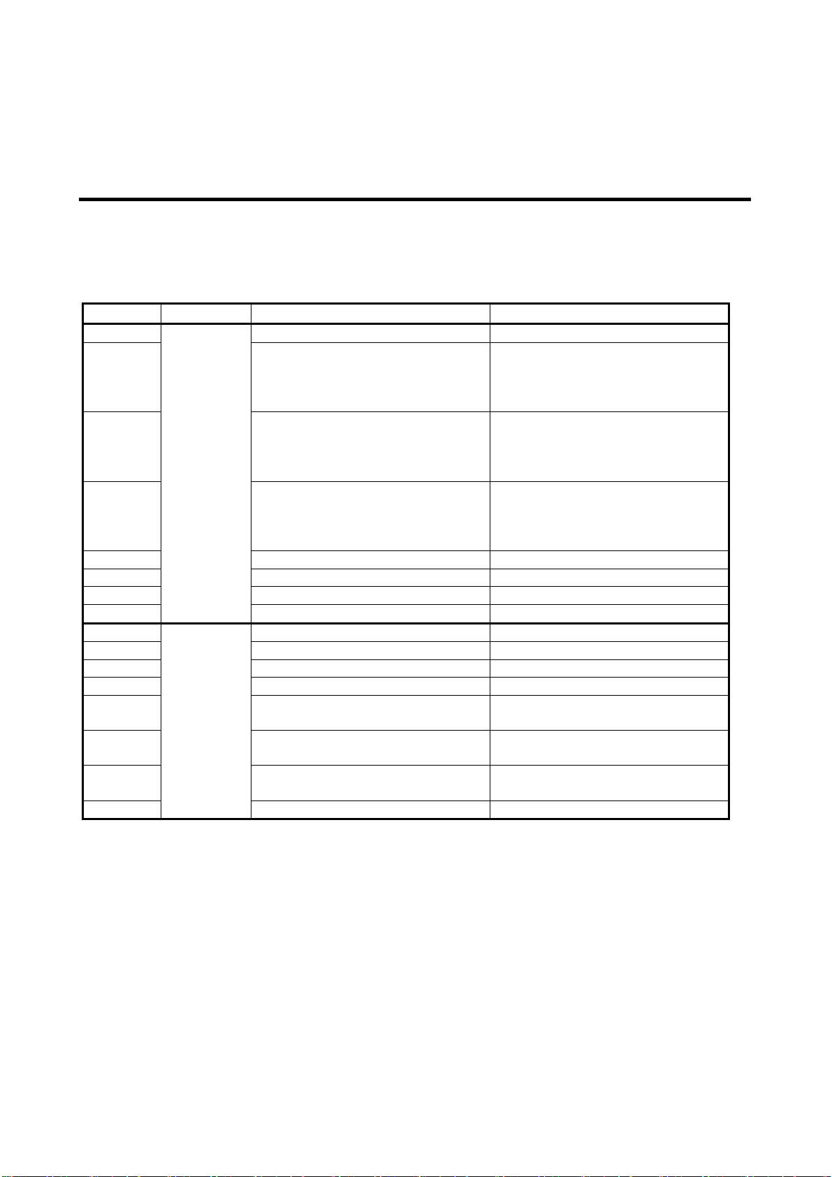
2. I/O Address Setting and Register
I/O port address of the board is automatically determined by the plug and play function (PnP function) of the PCI bus.
Read/Write registers of MCX304 on the board and ports of PIX132 can be accessed by API function which MC8000P device
driver provides. Each register and I/O port address are as shown in the table below.
For more details on each register, see chapter 4 of MCX304 user’s manual.
I/O Address IC Write Register Read Register
00 WR0 command register RR0 main status register
01
XWR1 X axis mode register 1
YWR1 Y axis mode register 1
ZWR1 Z axis mode register 1
UWR1 U axis mode register 1
XRR1 X axis status register 1
YRR1 Y axis status register 1
ZRR1 Z axis status register 1
URR1 U axis status register 1
02
XWR2 X axis mode register 2
YWR2 Y axis mode register 2
ZWR2 Z axis mode register 2
UWR2 U axis mode register 2
XRR2 X axis status register 2
YRR2 Y axis status register 2
ZRR2 Z axis status register 2
URR2 U axis status register 2
03
XWR3 X axis mode register 3
YWR3 Y axis mode register 3
ZWR3 Z axis mode register 3
UWR3 U axis mode register 3
XRR3 X axis status register 3
YRR3 Y axis status register 3
ZRR3 Z axis status register 3
URR3 U axis status register 3
04 WR4 output register 1 RR4 input register 1
05 WR5 output register 2 RR5 input register 2
06 WR6 write data register 1 RR6 read data register 1
07
MCX304
WR7 write data register 2 RR7 read data register 2
10 write prohibit invalid
11 write prohibit invalid
12 write prohibit invalid
13 write prohibit invalid
14 Port A output data
(Set to D7~D0)
Port A output data reading
(D7~D0)
15 Port B output data
(Set to D7~D0)
Port B output data reading
(D7~D0)
16 Port C output data
(Set to D7~D0)
Port C output data reading
(D7~D0)
17
PIX132
invalid invalid
- 3 -
NOVA electronics MC8022P/MC8042P - 4
3. I/O Signals
This chapter describes each I/O signals of the I/O connector. In the description, the signal name of each axis is described as
n○○○○.
3.1 CN2 Connector (Rear connector)
CN2 connector is equipped with external power (+24VDC) input, and inputs/outputs signals of each axis as shown below.
Connector Signal Type Signal Name
CN2
Drive pulse output signal in the +/– direction
Over run limit input signal in the +/– direction
Decelerating stop/Instant stop input signal 3 points
In-position and alarm input signal for servo motor
Deviation counter clear output signal for servo motor (shared with general
output 1 point)
nOUT0/DCC
Emergency stop input signal for all axis
nP+P/N, nP-P/N
nLMT+, nLMT-
nSTOP0, nSTOP1, nSTOP2
nINPOS, nALARM
EMG
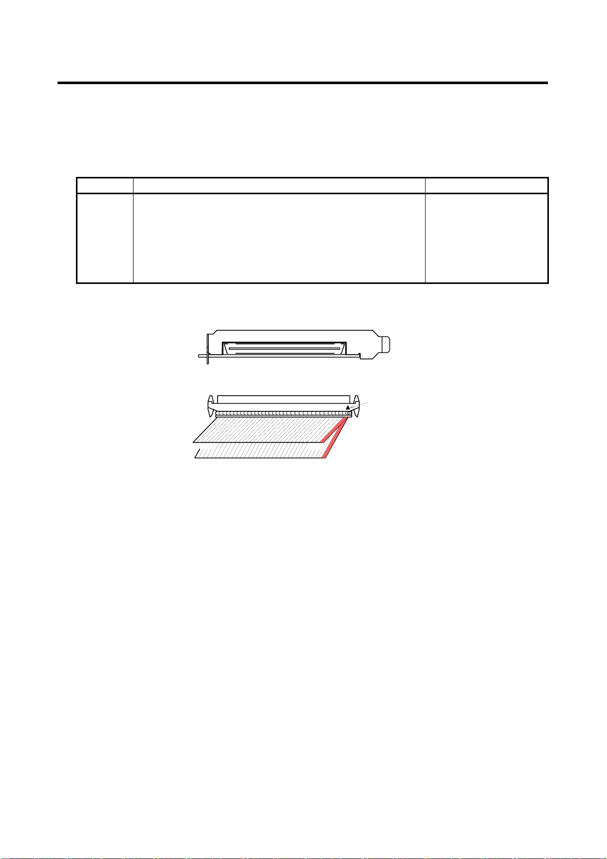
CN2 Connector Pin Assignments
A50 A49 A2 A1
B50 B49 B2 B1
Cable (included, 1.2m)
Pin 1 Mark
A1
B1
A50
B50
When implemented in PC, the connector may be upside down occasionally.
The cable (included) is A1, A2, … A49, A50 from the right (red) of the upper cable to the left, and B1, B2,
… B49, B50 from the right (red) of the lower cable to the left when Pin 1 mark (▲) of the connector is
placed in the upper right.
Connector type: Board side FX2B-100PA-1.27DS (Hirose), Cable side FX2B-100SA-1.27R (Hirose)
- 4 -

NOVA electronics MC8022P/MC8042P - 5
CN2 Connector
Pin Signal I/O Content Chapter
*Note2
Pin Signal I/O Content Chapter
A
1 VEX External Power (+24V) 3.12 B1 EMG Input Emergency Stop (All
axes)
3.11
A
2 XLMT+ Input X axis Limit in + direction 3.5
A
3 XLMT- Input X axis Limit in – direction 3.5
A
4 XSTOP0 Input X axis Decelerating Stop /
Instant Stop
3.6
A
5 XSTOP1 Input X axis Decelerating Stop /
Instant Stop
3.6
A
6 YLMT+ Input Y axis Limit in + direction 3.5
A
7 YLMT- Input Y axis Limit in – direction 3.5
A
8 YSTOP0 Input Y axis Decelerating Stop /
Instant Stop
3.6
A
9 YSTOP1 Input Y axis Decelerating Stop /
Instant Stop
3.6
A
10 ZLMT+ Input Z axis Limit in + direction 3.5 MC8042P
A
11 ZLMT- Input Z axis Limit in – direction 3.5 MC8042P
A
12 ZSTOP0 Input Z axis Decelerating Stop /
Instant Stop
3.6 MC8042P
A
13 ZSTOP1 Input Z axis Decelerating Stop /
Instant Stop
3.6 MC8042P
A
14 ULMT+ Input U axis Limit in + direction 3.5 MC8042P
A
15 ULMT- Input U axis Limit in – direction 3.5 MC8042P
A
16 USTOP0 Input U axis Decelerating Stop /
Instant Stop
3.6 MC8042P
A
17 USTOP1 Input U axis Decelerating Stop /
Instant Stop
3.6 MC8042P
A
18 XSTOP2 Input X axis Encoder Z-phase 3.7
A
19 XINPOS Input X axis Inposition 3.8
A
20 XALARM Input X axis Alarm 3.8
A
21 YSTOP2 Input Y axis Encoder Z-phase 3.7
A
22 YINPOS Input Y axis Inposition 3.8
A
23 YALARM Input Y axis Alarm 3.8
A
24 ZSTOP2 Input Z axis Encoder Z-phase 3.7 MC8042P
A
25 ZINPOS Input Z axis Inposition 3.8 MC8042P
A
26 ZALARM Input Z axis Alarm 3.8 MC8042P
A
27 USTOP2 Input U axis Encoder Z-phase 3.7 MC8042P
A
28 UINPOS Input U axis Inposition 3.8 MC8042P
A
29 UALARM Input U axis Alarm 3.8 MC8042P
A
30 GND Internal Circuit GND
A
31 XOUT0/DCC Output X axis General Output/DCC
*Note1
3.4
A
32 YOUT0/DCC Output Y axis General Output/DCC 3.4
A
33 ZOUT0/DCC Output Z axis General Output/DCC 3.4 MC8042P
A
34 UOUT0/DCC Output U axis General Output/DCC 3.4 MC8042P
A
35 XP+P Output X axis Drive Pulse in + direction 3.3
A
36 XP+N Output X axis Drive Pulse in + direction 3.3
A
37 XP-P Output X axis Drive Pulse in – direction 3.3
A
38 XP-N Output X axis Drive Pulse in – direction 3.3
A
39 YP+P Output Y axis Drive Pulse in + direction 3.3
A
40 YP+N Output Y axis Drive Pulse in + direction 3.3
A
41 YP-P Output Y axis Drive Pulse in – direction 3.3
A
42 YP-N Output Y axis Drive Pulse in – direction 3.3
A
43 ZP+P Output Z axis Drive Pulse in + direction 3.3 MC8042P
A
44 ZP+N Output Z axis Drive Pulse in + direction 3.3 MC8042P
- 5 -
NOVA electronics MC8022P/MC8042P - 6
A
45 ZP-P Output Z axis Drive Pulse in – direction 3.3 MC8042P
A
46 ZP-N Output Z axis Drive Pulse in – direction 3.3 MC8042P
A
47 UP+P Output U axis Drive Pulse in + direction 3.3 MC8042P
A
48 UP+N Output U axis Drive Pulse in + direction 3.3 MC8042P
A
49 UP-P Output U axis Drive Pulse in – direction 3.3 MC8042P
A
50 UP-N Output U axis Drive Pulse in – direction 3.3 MC8042P
*Note1: DCC (Deviation Counter Clear): Output to clear the deviation counter of a servo motor driver.
*Note2: MC8042P: The signals which only MC8042P has. MC8022P doesn’t.
Note: When connecting or disconnecting the cable into the CN2 connector, turn OFF PC first and turn OFF external
power (DC+24V), then connect or disconnect the cable. Otherwise, the destruction of the internal circuit may be
caused. Be careful about the connector direction and not to reverse it.
3.2 CN3, 4 Connector (Connector on the board)
CN3, 4 connectors on the board input/output signals of each axis as shown below.
Connector Signal Type Signal Name
CN3
Driving by external input signal in the +/– direction (can be used as general
input)
Encoder A/B phase input signal
nEXOP+, nEXOP–
nECAP/N, nECBP/N
CN4 General output signal OUT1~14
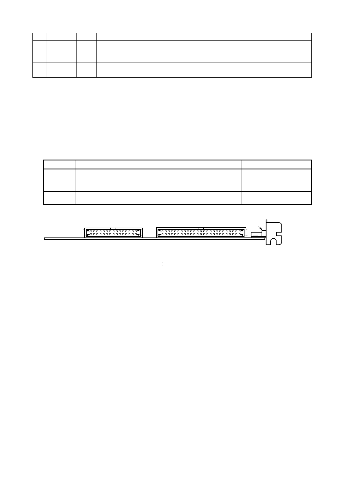
CN3, 4 Connector Pin Assignments
CN3(50P)CN4(30P) 1
2
49
50
29
30
1
2
CN2
Mounting face
Rear face
Connector: HIF3FC-30PA-2.54DS (Hirose)
Socket (included): HIF3BA-30D-2.54R
(Optional accessor
y
Connector: HIF3FC-50PA-2.54DS (Hirose)
Socket (included): HIF3BB-50D-2.54R
(Optional accessory)
- 6 -
NOVA electronics MC8022P/MC8042P - 7
CN3 Connector
Pin Signal I/O Content Chapter Pin Signal I/O Content Chapter
1 VEX External Power(+24V)3.12 2 VEX External Power(+24V)3.12
3
X
EXOP+ Input X axis Driving by External
Signal in + direction 3.10 4 XEXOP- Input X axis Driving by External
Signal in - direction 3.10
5
Y
EXOP+ Input Y axis Driving by External
Signal in + direction 3.10 6 YEXOP- Input Y axis Driving by External
Signal in - direction 3.10
7
Z
EXOP+ Input Z axis Driving by External
Signal in + direction
3.10
*Note2 8 ZEXOP- Input Z axis Driving by External
Signal in - direction
3.10
*Note2
9 UEXOP+ Input U axis Driving by External
Signal in + direction
3.10
*Note2 10 UEXOP- Input U axis Driving by External
Signal in - direction
3.10
*Note2
11 12
13 14
15 16
17 18
19
X
ECAP Input X axis Encoder A phase (+) 3.9 20 XECAN Input X axis Encoder A phase (–) 3.9
21
X
ECBP Input X axis Encoder B phase (+) 3.9 22 XECBN Input X axis Encoder B phase (–) 3.9
23
Y
ECAP Input Y axis Encoder A phase (+) 3.9 24 YECAN Input Y axis Encoder A phase (–) 3.9
25
Y
ECBP Input Y axis Encoder B phase (+) 3.9 26 YECBN Input Y axis Encoder B phase (–) 3.9
27
Z
ECAP Input Z axis Encoder A phase (+) 3.9
*Note2 28 ZECAN Input Z axis Encoder A phase (–) 3.9
*Note2
29
Z
ECBP Input Z axis Encoder B phase (+) 3.9
*Note2 30 ZECBN Input Z axis Encoder B phase (–) 3.9
*Note2
31 UECAP Input U axis Encoder A phase (+) 3.9
*Note2 32 UECAN Input U axis Encoder A phase (–) 3.9
*Note2
33 UECBP Input U axis Encoder B phase (+) 3.9
*Note2 34 UECBN Input U axis Encoder B phase (–) 3.9
*Note2
35 36
37 38
39 40
41 42
43 44
45 46
47 48
49 50
*Note2: MC8042P: The signals which only MC8042P has. MC8022P doesn’t.
CN4 Connector
Pin Signal I/O Content Chapter Pin Signal I/O Content Chapter
1 VEX External Power(+24V)3.12 2 VEX External Power(+24V)3.12
3 4
5 6
7 8
9 OUT1/PA6 Output General Output1 3.4 10 OUT2/PA7 Output General Output2 3.4
11 OUT3/PB0 Output General Output3 3.4 12 OUT4/PB1 Output General Output4 3.4
13 OUT5/PB2 Output General Output5 3.4 14 OUT6/PB3 Output General Output6 3.4
15 OUT7/PB4 Output General Output7 3.4 16 OUT8/PB5 Output General Output8 3.4
17 OUT9/PB6 Output General Output9 3.4 18 OUT10/PB7 Output General Output10 3.4
19 OUT11/PC0 Output General Output11 3.4 20 OUT12/PC1 Output General Output12 3.4
21 OUT13/PC2 Output General Output13 3.4 22 OUT14/PC3 Output General Output14 3.4
23 24
25 26
27 GND Internal Circuit GND 28 GND Internal Circuit GND
29 GND Internal Circuit GND 30 GND Internal Circuit GND
- 7 -
NOVA electronics MC8022P/MC8042P - 8
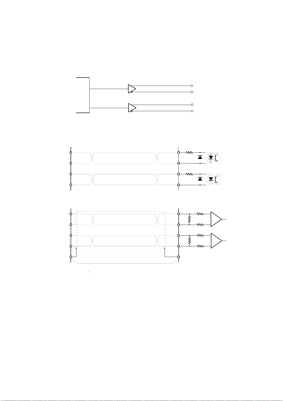
3.3 Drive Pulse Output Signal (nP+P, nP+N, nP-P, nP-N)
Drive pulse output signal outputs the drive pulse of +/– direction of MCX304 through a differential line-driver output
(AM26C31 or equivalent). nP+N is the reverse output of nP+P and nP-N is the reverse output of nP-P. At resetting, positive
output (nP+P, nP-P) becomes low level and reverse output (nP+N, nP-N) becomes hi level. Drive pulse output is set to
independent 2-pulse type after resetting; however, the user can change to 1-pulse 1-direction type in mode setting. See chapter
2.6.2 and 4.5 of MCX304 user’s manual.
MCX304
AM26C31C or equivalent
nP+P
nP+N
nP- P
nP- N
nPP/PLS
nPM/DIR
Drive Pulse Output Signal Circuit
The following is the connection example of a motor driver with a photo coupler input and line receiver input.
AXP+P
AXP+N
AXP- P
AXP- N
CW+
CW-
CCW+
CCW-
Motor driver
MC8022P/MC8042P
Connection example of a motor driver with a photo coupler input
AXP+P
AXP+N
AXP-P
AXP- N
CW+
CW-
CCW+
CCW-
Motor driver
+
-
+
-
AM26LS32
AM26LS32
Twist Pair Shield
GND GND
Signal GND Line
Connection example of a motor driver with a line receiver input
Note1: As shown above, when using a line receiver input circuit, connect MC8022P/MC8042P and a motor driver with GND
line. If there is the potential difference between MC8022P/MC8042P and motor driver, the malfunction and destruction of a
driver circuit and/or a motor driver circuit may be caused.
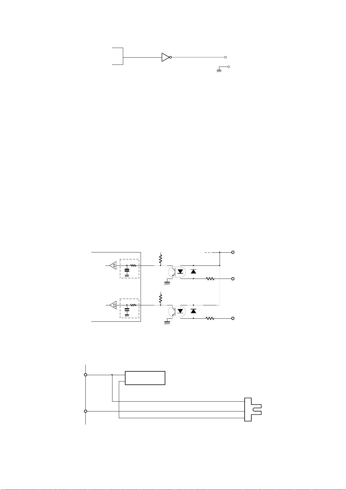
3.4 General Output Signal and Deviation Counter Clear Output Signal (OUT1~14, nOUT0/DCC)
General output signal outputs 14 points from PIX132 and one nOUT0/DCC output signal in MCX304 through buffer (TD62503).
nOUT0 signal is shared with deviation counter clear output (DCC) and is output from CN2 connector. Also other general output
signals: OUT1~14 are output from CN4 connector. At resetting, all the output signals (open collector output) will be OFF.
- 8 -
NOVA electronics MC8022P/MC8042P - 9
■ OUT1~14 Output
PIX132
GND
TD62503
OUT1
OUT14
Port Output
in out
2.7K
10K
TD62503(Toshiba)internal circuit
Output voltage:35V(max)
Output current:100mA(max)
Port Output
・
・
・
・
・
・
・
・
・
・
General Output Circuit
OUT1~14 general output signals are output from CN4. ON/OFF of this signal can be controlled by writing to each port of PIX132
(NOVA electronics). Each port is set to output and becomes OFF when the PC system is started.
General Output Signal(CN4pin),Register Bit Table
CN4 PIX132
Pin # Output signal Port address Bit position
9
10
11
12
13
14
15
16
17
18
19
20
21
22
OUT1
OUT2
OUT3
OUT4
OUT5
OUT6
OUT7
OUT8
OUT9
OUT10
OUT11
OUT12
OUT13
OUT14
0x14
0x14
0x15
0x15
0x15
0x15
0x15
0x15
0x15
0x15
0x16
0x16
0x16
0x16
6
7
0
1
2
3
4
5
6
7
0
1
2
3
ON/OFF of OUT1~14 output signals can be controlled by the following steps (1)~(4) on the program.
(1) Read current output data.
・Check the port address of the signal which the user wants to output and bit position according to the table above.
・Read the current output of the port.
Function: Nmc_InPort Current output data: mcb0pa
mcb0pa = Nmc_InPort(Board number, Port address);
0x14, 0x15, 0x16
0x0~0xF
Example) Read the output data of the port which includes OUT1 output signal. mcb0pa = Nmc_InPort(0x0, 0x14);
(2) When turning ON the output.
・Set 1 to the bit corresponding to the signal which the user wants to turn ON.
・Example) When turning ON OUT1 output signal
mcb0pa = mcb0pa | 0x40; (OUT1 is bit position 6, OR bit pattern is 0x40.)
(3) When turning OFF the output.
・Set 0 to the bit corresponding to the signal which the user wants to turn OFF.
・Example) When turning OFF OUT1 output signal.
mcb0pa = mcb0pa & 0xbf; (OUT1 is bit position 6, AND bit pattern is 0xbf.)
(4) Set the output data.
・Write the output data which is calculated by (2) or (3) to the port.
Function: Nmc_OutPort(Board number, Port address, Output data);
Example) Write the output data to the port Nmc_OutPort(0x0, 0x14, mcb0pa);
Examples of ON/OFF control of general output signals are described in sample program, so refer to it.
- 9 -
NOVA electronics MC8022P/MC8042P - 10
■ nOUT0/DCC Output
MCX304
nOUT0/DCC
GND
TD62503(Toshiba)
nDRIVE/
OUT0/DCC
nOUT0/DCC output is shared with general output signal (nOUT0) and deviation counter clear output (DCC), and is output to CN2.
At resetting, it will be OFF. Control of this signal is different from other general output, it can be performed by writing to the
register of MCX304.
When used as general output.
(1) To enable nOUT0 output, set the nOT0E bit of MCX304/WR5 to 1.
(2) Turn ON: Set the nOUT0 bit of MCX304/WR4 to 1. Turn OFF: Set the nOUT0 bit of MCX304/WR4 to 0.
When used as deviation counter clear output.
Deviation counter clear output is the output to clear a deviation counter in a servo motor driver. MCX304 has the function to
output this deviation counter clear signal during automatic home search.
For setting of a deviation counter clear enable, a logical level and pulse width, see chapter 2.4.3 of MCX304 user’s manual. And
for automatic home search details, see chapter 2.4. As shown in the figure above, TD62503 is used as buffer on the board, so that
the board output (open collector) turns ON when MCX304 output is active Hi.
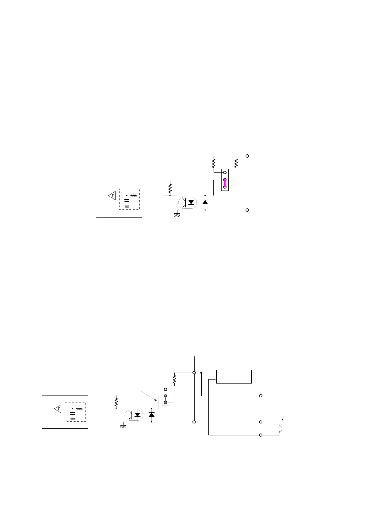
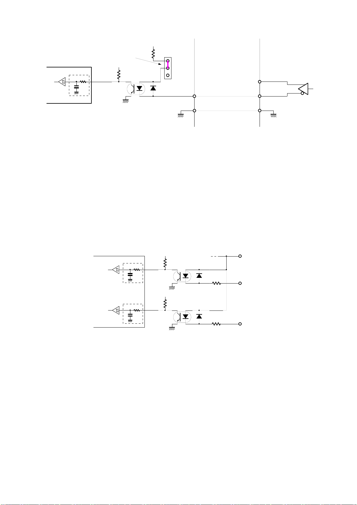
3.5 Over Run Limit Input Signal (nLMT+, nLMT-)
It is the input signal to stop each drive pulse in the +/ – direction. This input signal is connected to the limit input of MCX304
through a photo coupler. After resetting, MCX304 becomes low active, so limit function works when electric current flows from a
signal pin (nLMT+, nLMT-). For more details on mode setting, see chapter 4.5 of MCX304 user’s manual.
To enable this signal, external power supply DC24V is needed. When the board is powered on, a built-in filter of this signal
becomes the setting of signal delay time 512μsec as default. This signal delay time can be changed for circumstances of system
noise. For more details, see chapter 2.6.9 and 4.6 of MCX304 user’s manual.
VEX(+24V)
+5V
MCX304
10K
nLMTP
nLMTM
nLMT+
+5V
nLMT-
8.2K
TLP281 or equivalent
Delay time: 512µSEC (default)
Built- in filter
Built- in filter
Over Run Limit Input Signal Circuit
The connection example of an over run limit input signal and a photo microsensor is shown below. When D3 bit of X axis mode
register 2 (XWR2) is set to 0 (the mode at reset), limit function becomes active at the light interception.
DC24V Power
+
-
+
L
OUT
-
EE- SX670(Omron)
Active at the light interception
VEX
AXLMT+
MCX304 X axis mode register 2 WR2/D3 bit:0
MC8022P/
MC8042P
Connection Example of Over Run Limit Input Signal and Photo Microsensor
When long wiring is needed, use the shield cable.
- 10 -
NOVA electronics MC8022P/MC8042P - 11
3.6 Decelerating Stop / Instant Stop (nSTOP0, nSTOP1)
Input signal to stop drive pulse output in deceleration or immediately. Generally, nSTOP0 signal is used as a near home signal and
nSTOP1 signal is used as a home signal. MCX304 has three signals, STOP2~STOP0 for each axis as a home search input signal;
however, STOP2 is equipped with an interface circuit for encoder Z-phase. STOP1 signal is used as an input signal for home and
STOP0 is for near home.
[Enable/Disable and Logical setting]
Each input signal can be set enable/disable and logical level in mode setting. When enable is set in mode setting, and when this
signal becomes active during driving, drive pulse output stops. When during acceleration/deceleration driving, it stops in
deceleration and when during constant driving, it stops immediately. After resetting, all the signals are disabled. For instant, when
D1, D0 bit of XWR1 register is set to 1, 0 and set to low level and enable, and when current flows out from XSTOP0 signal pin
(CN2-A4) of this board, driving stops. For more details on mode setting, see chapter 4.4 of MCX304 user’s manual.
[Automatic Home Search]
MCX304 has automatic home search function. See chapter 2.4 of MCX304 user’s manual.
To perform high-speed home search →low-speed home search by only one signal, use nSTOP0 signal and switch JP3 jumper to
UPPER side as follows:
VEX (+24V)
+5V
MCX304
10K
nSTOP0
nSTOP1
nSTOP0
+5V
nSTOP1
8.2K
TLP281 or equivalet
Built- in filter
Built- in filter JP3
Factory setting
LOWER
UPPER
Delay time:
512µSEC(Default)
Decelerating Stop/ Instant Stop Input Signal Circuit
To enable this signal, external power supply DC24V is needed. When the board is powered on, a built-in filter in this signal
becomes the setting of signal delay time 512μsec as default. This signal delay time can be changed for circumstances of system
noise. For more details, see chapter 2.6.9 and 4.6 of MCX304 user’s manual.
This signal can read out the signal status by input register 1, 2 (RR4, 5) at any time, so it can be used as general input.
- 11 -
NOVA electronics MC8022P/MC8042P - 12
3.7 Encoder Z-phase Input Signal (nSTOP2)
nSTOP2 input signal is to stop drive pulse output during driving by connecting to the Z-phase output signal of an encoder or a
servo motor driver.
To enable this signal, external power supply DC24V is needed. When the board is powered on, a built-in filter in this signal
becomes the setting of signal delay time 512μsec as default. This signal delay time can be changed for circumstances of system
noise. For more details, see chapter 2.6.9 and 4.6 of MCX304 user’s manual.
[Enable/Disable and Logical setting]
nSTOP2 signal can be set enable/disable and logical level in mode setting as well as nSTOP1, 0 signal. For instant, when D5, D4
bit of WR1 register is set to 1, 0 and set to low and enable, and when current flows out from nSTOP2 signal pin of this board,
driving stops. For more details on mode setting, see chapter 4.4 of MCX304 user’s manual.
[Jumper setting]
This input signal can be adapted to either open collector output or line-driver output of the other output side by switching JP4
jumper. When the other side is open collector output, set JP4 to LOWER side (factory setting) and when is line-driver output, set
JP4 to UPPER side and connect nSTOP2 signal to one side of line-driver output.
VEX (+24V)
+5V
MCX304
8.2K
TLP281 or equivalent
10K
nSTOP2
nSTOP2
Built- in filter
Delay time: 512µSEC(default)
JP4
1K
+5V
(Factory setting)
UPPER
LOWER
Encoder Z-phase Input Signal Circuit
[Notes on Z-phase search]
Drive speed of Z-phase search
When this board is powered on, a built-in filter of nSTOP2 signal becomes the setting of signal delay time 512μsec as default. In
addition, TLP281 photo coupler (Toshiba) has approximately 100μsec delay time, so that the drive speed to search Z-phase must
be set for Z-phase signal to be active more than 1msec at least. When noise circumstances are good, search operation can be
performed at the higher speed by disabling the built-in filter of STOP2 signal.
Starting position for Z-phase search
In automatic home search of MCX304, the function stops search driving when the Z-phase signal (nSTOP2) changes from inactive
to active. Therefore, the starting position for Z-phase search must be completely away from this change point. Normally, adjust
mechanically so that this starting position becomes the 180°opposite side to the encoder Z-phase position.
The connection example of nSTOP2 input signal and open collector output of an encoder is shown below. When open collector
output is ON at Z-phase detected, set the D4 bit (SP2-L) of WR1 register to 0 (state of reset) for logical setting of MCX304.
DC24Vpower
+
-
VEX
+5V
MCX304
8.2K
TLP281 or equivalent
10K
nSTOP2
nSTOP2
Built- in filter
JP4
Encoder
VCC
EC- Z
GND
Open collector output
LOWER
JP4: Set to LOWER side
MC8022P/
MC8042P
Connection Example with Z-phase Output of open collector
The following is the connection example of nSTOP2 input signal and one pin of line-driver output of an encoder. When output is
low level at Z-phase detected, set the D4 bit (SP2-L) of WR1 register to 0 (state of reset) for logical setting of MCX304.
- 12 -
NOVA electronics MC8022P/MC8042P - 13
JP4:Set to UPPER side
UPPER
+5V
MCX304
TLP281 or equivalent
10K
nSTOP2
nSTOP2
Built- in filter
JP4
1K
+5V
EC- Z
Encoder
GND GND
MC8022P/
MC8042P
Connection Example with Z-phase Output of line-driver
3.8 Input Signals for Servo Motor (nINPOS, nALARM)
nINPOS input signal is applied to the in-position output of a servo motor driver. Enable/disable and logical level can be set in
mode setting of MCX304. When enable is set and after completion of the driving, nDRV bit of main status register (RR0) returns
to 0 after this signal becomes active.
nALARM input signal is applied to the alarm output from a servo motor driver. Enable/disable and logical level can be set in
mode setting. When enable is set, nALARM input signal is monitored, and when nALARM is active, the ALARM bit of status
register 2 (nRR2) is set to 1. When the signal becomes active during driving, driving will stop immediately.
After resetting, both signals are disabled. For nINPOS input signal, set the D15, 14 bit of mode register 2 (nWR2) of MCX304 to
1,0 as low level active, and the n-DRV bit of RR0 register returns to 0 after waiting to flow current from nINPOS signal. For
nALARM input signal, set the D13, 12 bit of nWR2 register to 1,0 as low level active, and the signal becomes an alarm state when
current flows from nALARM signal pin. For more details, see chapter 2.6.5 and 4.5 of MCX304 user’s manual.
nINPOS
nALARM
nINPOS
nALARM
VEX (+24V)
+5V
MCX304
10K
+5V
8.2K
TLP281 or equivalent
Delay time: 512µSEC (default)
Built- in filter
Built- in filter
Input Signal Circuit for Servo Motor
To enable this signal, external power supply DC24V is needed. When the board is powered on, a built-in filter in this signal
becomes the setting of signal delay time 512μsec as default. This signal delay time can be changed for circumstances of system
noise. For more details, see chapter 2.6.9 and 4.6 of MCX304 user’s manual.
In addition, the input signal for a servo motor can read out the signal status by input register 1, 2 (RR4, 5) at any time, so it can be
used as general input.
- 13 -
NOVA electronics MC8022P/MC8042P - 14
3.9 Encoder A/B phase Input Signal (nECAP, nECAN, nECBP, nECBN)
nECAP/N, nECBP/N, input signals are the input to count a real position counter of MCX304 by connecting to the 2-phase output
signal of an encoder or a servo motor driver. For more details, see chapter 2.3.1, 2.6.3 and 4.5 of MCX304 user’s manual.
MCX304
nECA/PPIN
nECB/PMIN
TLP115A
1K 220 nECAP
nECAN
nECBP
nECBN
+5V
750
+5V
Encoder A/B phase Input Signal Circuit
As shown above, encoder A/B phase input signal circuit uses high-speed photo coupler IC TLP115A (Toshiba). Each input signal
can be directly connected to a differential line-driver output. As the figure below, when n***P/N signal is H/L, n*** signal of
MCX304 becomes Low and when is L/H, it becomes Hi. The delay time from input to the signal pin of MCX304 is under
100nSEC, so that the signal can count up to 4MHz in the case of 2-phase pulse input.
n***P
n***N
n***
Input Signal
MCX304 Signal
H
L
L
H
LH
The connection example of an encoder A/B phase input signal and a differential line-driver output is shown as follows:
XECAP
XECAN
XECBP
XECBN
EC- A
EC- B
AM26LS31
Encoder
CN3
MC8022P/
MC8042P
Connection Example with Differential line-driver Output
The connection example of an encoder A/B phase input signal and an encoder with open collector output is shown as follows:
Encoder
VCC
EC- A
EC- B
GND
DC Power
+
-
XECAP
XECAN
XECBP
XECBN
R
R
Power Voltage(V) R(
Ω)
5
12
24
0
820 1/4W
2K 1W
CN3
MC8022P/
MC8042P
Connection Example with Open Collector Output
- 14 -
NOVA electronics MC8022P/MC8042P - 15
3.10 Driving by External Signal (nEXOP+, nEXOP-)
The signal externally controls driving in the + or – direction. In fixed driving mode, the falling edge of these signals trigger
outputs specified drive pulse. In continuous driving mode, drive pulse is output continuously while the input signals are low. This
function can reduce the load of the host CPU, so the user can perform jog feed of each axis speedy. External signal for driving can
be set in mode setting of MCX304. For more details, see chapter 2.6.1 and 4.6 of MCX304 user’s manual.
nEXPP
nEXPM
nEXOP+
nEXOP-
VEX (+24V)
+5V
MCX304
10K
+5V
8.2K
TLP281 or equivalent
Delay time: 512µSEC (default)
Built- in filter
Built- in filter
External Driving Signal(nEXOP+/-) Circuit
To enable this signal, external power supply DC24V is needed. When the board is powered on, a built-in filter in this signal
becomes the setting of signal delay time 512μsec as default. This signal delay time can be changed for circumstances of system
noise. For more details, see chapter 2.6.9 and 4.6 of MCX304 user’s manual.
3.11 Emergency Stop Input Signal (EMG)
All the drive pulse output stops when emergency stop signal becomes active. Active level can be switched by the JP2 jumper pin
on the board. When emergency stop signal becomes active during driving, driving for all axes stops instantly and 1 is set to the
error bit of all axes of main status register. For emergency stop of MCX304, see chapter 2.6.6 and 4.1.2 of MCX304 user’s
manual.
VEX (+24V)
+5V
MCX304
8.2K
TLP281 or equivalent
10K
74HC14 or equivalent
EMGN
EMG
JP2 2
1
4
3
JP2:EMG level switching
Built- in filter
(1- 2 short- circuited
in factory default)
Emergency Stop Input Signal Circuit
To enable this signal, external power supply DC24V is needed. When the board is powered on, a built-in filter in this signal
becomes the setting of signal delay time 512μsec as default. This signal delay time can be changed for circumstances of system
noise. For more details, see chapter 2.6.9 and 4.6 of MCX304 user’s manual.
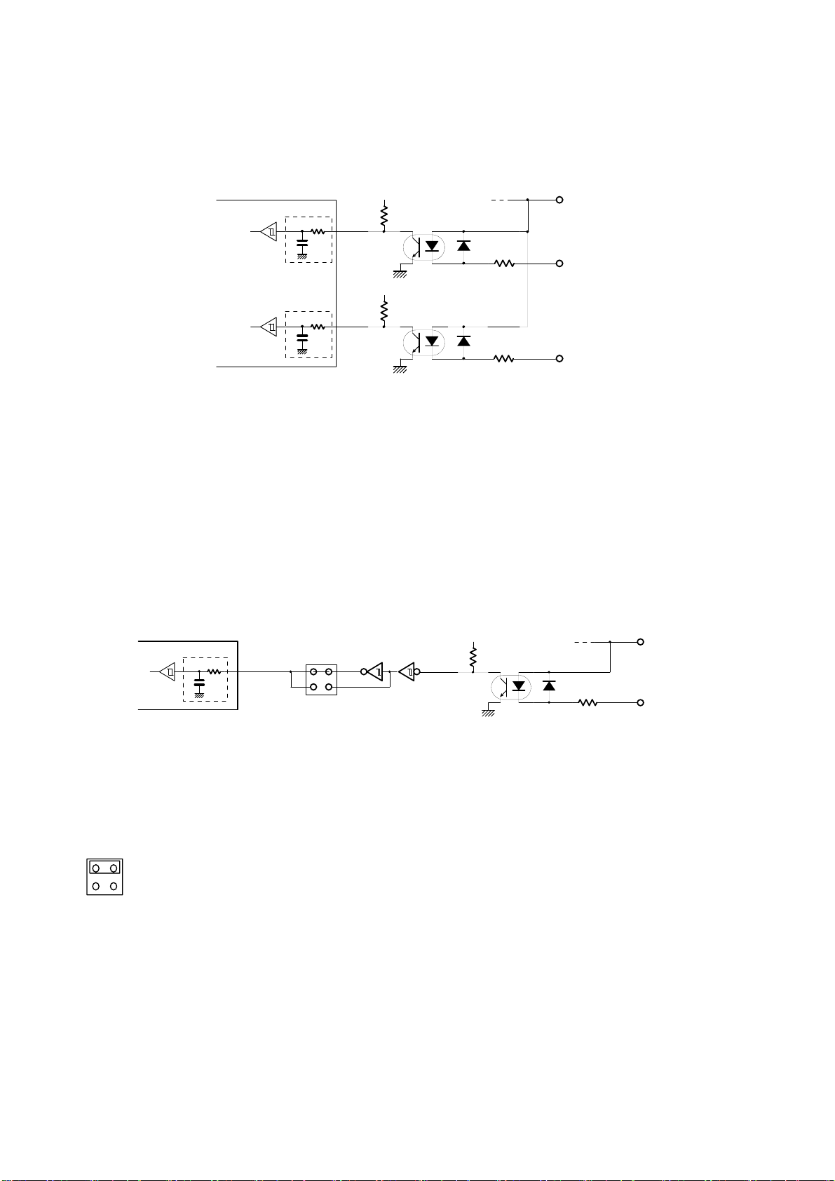
Pin assignments of the JP2 jumper is shown on the left.
1-2 short circuit: When emergency stop signal (EMG) is short-circuited with GND of the external power, it becomes
active.
JP2
1
34
2
3-4 short circuit: When emergency stop signal (EMG) is open, it becomes active.
Factory default is 1-2 short-circuited.
3.12 External Power (VEX)
The power supplied externally is used for over run limit input signal (nLMT+, nLMT–) of each axis, decelerating stop/instant stop
(nSTOP0, nSTOP1, nSTOP2) input signal, input signal for servo motor (nINPOS, nALARM), external signal for driving
(nEXOP+, nEXOP–) and emergency stop input signal (EMG). DC24V is needed. Consumption current is 2.8mA per 1 input
signal.
- 15 -

NOVA electronics MC8022P/MC8042P - 16
4. Interrupt
This board has an interrupt signal generated by MCX304, which connect to the INTA# of four interrupt request signals in the
PCI bus. When an interrupt occurs in MCX304, the interrupt request signal of this board changes from Hi to Low. By reading
out the status register 3 (nRR3) of the axis generated the interrupt, the interrupt request signal returns from Low to Hi.
For the interrupt function of MCX304, please refer to the following.
Article Reference manual
Function of the interrupt Chapter 2.5 of MCX304 user’s manual
Setting of the interrupt enable / disable Chapter 4.4 of MCX304 user’s manual
Interrupt notion to the application MC8000P User’s manual of device driver
When handling the interrupt by VC in Chapter 3.4.3
Chapter 4.13 of MCX304 user’s manualReading out of the interrupt generation MC8000P User’s manual of device driver
When handling the interrupt by VC in Chapter 3.4.3
[Notes for using interrupt]
IRQ number for the interrupt signal of this board is determined depending on PnP function.
In addition, it shares the same interrupt request signal with other devices by PnP function and Windows, competition is not
occurred because Windows generally controls it.
- 16 -
This manual suits for next models
1
Table of contents
Popular PCI Card manuals by other brands


Netis
Netis WF-2113 user manual

Curtiss-Wright
Curtiss-Wright FibreXtreme SL100 user guide

Atlantis Land
Atlantis Land 1066 A02-WP-54G GE01 quick start guide

AXAGO
AXAGO PCEA-P1 Quick installation guide

Renkforce
Renkforce 1616188 operating instructions

National Instruments
National Instruments NI PCIe-8360 Setup

Linksys
Linksys WMP11 ver. 2.7 Quick installation

Sonnet
Sonnet PRESTO 10GbE 10GBASE-T quick start guide

StarTech.com
StarTech.com PCISCSIU2W instruction manual

Moxa Technologies
Moxa Technologies CP-102U Series Quick installation guide

WinFast
WinFast DTV1000 S Quick installation guide

ICP DAS USA
ICP DAS USA PISO-DNM100-D user manual