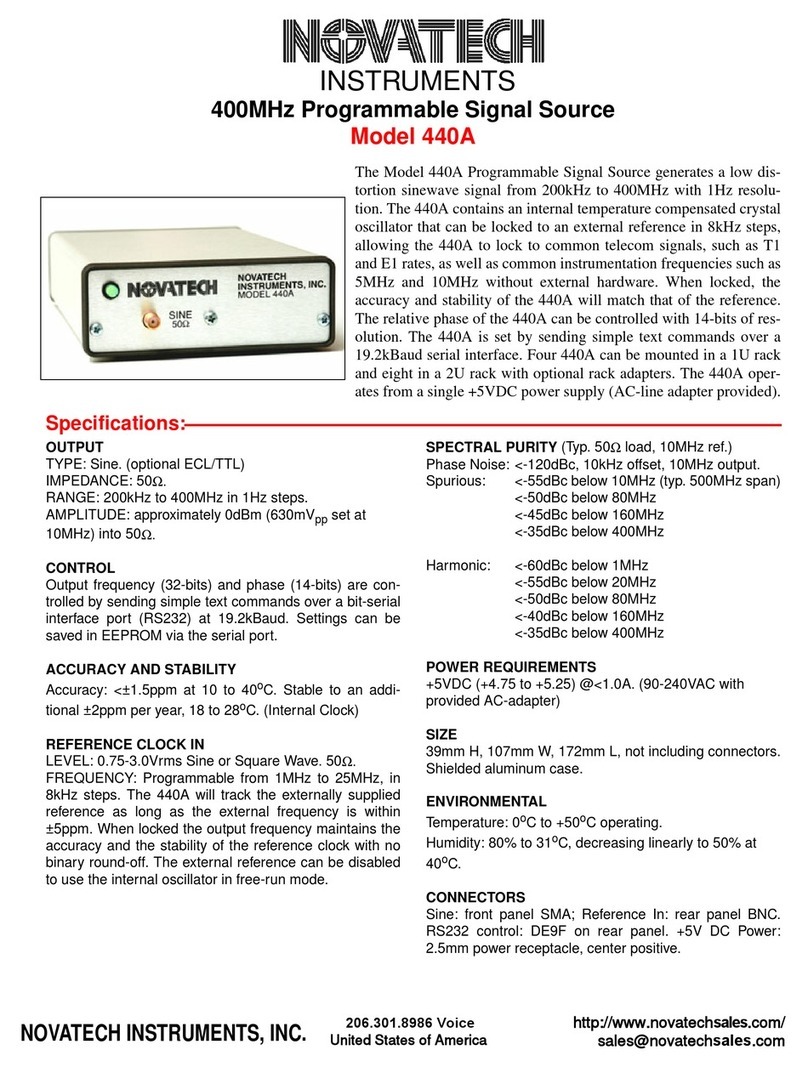
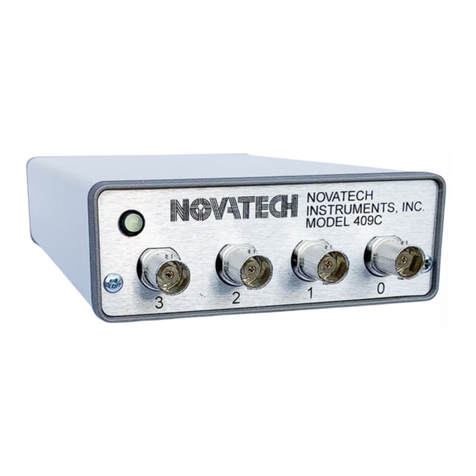
Novatech Instruments 408A User manual

NOVATECH INSTRUMENTS
1
408A Manual
INSTRUCTION MANUAL
Model 408A 100MHz Quadrature Signal Generator
408A
Table of Contents
Section
Page
Contents
1.0
. . . . . . . . . . . . . . . . . . . . . . . . . . . . .
2
. . . . . . . . . . . . . . . . . . . . . . . . .
Description
2.0
. . . . . . . . . . . . . . . . . . . . . . . . . . . . .
2
. . . . . . . . . . . . . . . . . . . . . . .
Specifications
3.0
. . . . . . . . . . . . . . . . . . . . . . . . . . . . .
3
. . . . . . . . . . . .
408A Hardware Installation
4.0
. . . . . . . . . . . . . . . . . . . . . . . . . . . . .
5
. . . . . . . . . . . . . . . . . . . . . . . . . . .
Operation
5.0
. . . . . . . . . . . . . . . . . . . . . . . . . . . . .
6
. . . . . . . . . . . . . . . . . .
Theory of Operation
6.0
. . . . . . . . . . . . . . . . . . . . . . . . . . . . .
8
. . . . . . . . . . . . . . . . . . . . .
Performance Test
7.0
. . . . . . . . . . . . . . . . . . . . . . . . . . . . .
9
. . . . . . . . . . . . . . . . . . . . . . . . . .
Calibration
--
. . . . . . . . . . . . . . . . . . . . . . . . . . . . . . .
10
. . . . . . . . . . . . . . . . . . . . . . . . . . .
Warranty
INSTRUMENTS

2
408A Manual
1.0
DESCRIPTION
1.1 The Model 408A is a 100MHz Quadrature
D
irect
D
igital
S
ynthesizer (DDS) in a small table
top case with RS232 serial control. The 408A pro-
vides both Cosine(I), Sine(Q) and 3.3V ACMOS
output signals, which can be set from 100Hz to
100MHz in 1µHz steps when using the internal
VCTCXO (voltage controlled temperature compen-
sated crystal oscillator) clock.
1.2 The 408A can also be used with an External
Clock input. An on-board programmable frequency
multiplier generates the master clock allowing user
configured frequency ranges. The multiplier can be
disabled for direct inputs up to 300MHz for opti-
mum phase noise performance. When used with an
external clock, multiple 408A are phase synchro-
nous.
2.0
SPECIFICATIONS
2.1 OUTPUTS
TYPES: Sine, Cosine and ACMOS/TTL Simulta-
neously.
IMPEDANCE: 50Ω.
FREQUENCY:100Hz to 100MHz in 1µHz steps,
using Internal Clock. (1x10-13 resolution @10MHz)
2.2 SINE/COSINE AMPLITUDE
AMPLITUDE: Approximately 0.5Vrms (+7dBm)
into 50Ω. Programmable from 0/4096 to 4095/4096
of Full Scale (12 Bits).
FLATNESS: ±3dB from 100kHz to 100MHz refer-
enced to amplitude at30MHz, stable to ±1dB from
18-28 oC.
2.3 ACMOS/TTL AMPLITUDE
VOL<0.5V, VOH>2.5V into a 15pF load, series ter-
minated. Rise and Fall Times <5ns. Duty Factor: 45-
55%. 50Ωoutput impedance. Use series or capaci-
tively-coupled parallel termination.
2.4 ACCURACY AND STABILITY
Accurate to <±1.5ppm at 10-40oC. Stable toanaddi-
tional ±2ppm per year, 18-28oC.
NOVATECH INSTRUMENTS
2.5 EXTERNAL CLOCK INPUT
LEVEL: 0.35-2.5Vrms Sine or Square Wave can be
applied to the EXT CLK Input BNC. 50Ω.
FREQUENCY: Input range of 5MHz to 75MHz.
Programmable frequency multiplier (4x to 20x) on
board. Multiplier can be bypassed for direct input to
300MHz. An external filter may be required for
optimum performance.
2.6
SPECTRAL PURITY
(Typ. 50Ωload, int clk)
Phase Noise: <-140dBc, 10kHz offset, 5MHz out.
Spurious: <-70dBc below 10MHz (200MHz span)
<-65dBc below 40MHz
<-60dBc below 60MHz
<-50dBc below 100MHz
Harmonic: <-70dBc below 1MHz
<-60dBc below 10MHz
<-50dBc below 20MHz
<-40dBc below 50MHz
<-35dBc below 100MHz
2.7 CONTROL
Output Frequency and phase (14-bits) are controlled
by an RS232 serial port at 19.2kBaud. RS232 con-
trol allows non-volatile storage of settings.
2.8 SWITCHING TIME
RS232 control depends upon host speed and com-
mands sent, typically <10ms for a new frequency.
2.9
POWER REQUIREMENTS
+4.5 to +5.5VDC @<1.25A. Line voltage adapter
provided. (Units with serial numbers before N06001
used +12V nominal).
2.10
SIZE
Table top case: 40mm H, 106mm W, 172mm L,
excluding connectors.
2.11 CONNECTORS
Front panel BNCs for SINE(Q), COSINE(I) and
ACMOS/TTL. Rear panel BNC for EXT CLK IN.
Power: 2.5mm center positive. DE9F for serial.

3
408A Manual
3.0
HARDWARE INSTALLATION
3.1
Power Connection.
Insert 2.5mm plug from
AC-adapter into the receptacle on the rear panel.
The 408A requires a nominal +5VDC. Then plug the
AC-adapter into your AC-line source.
NOTE:
Use only the AC line power adapter provided with
your 408A.
3.2
RS232 Installation.
To use the 408A connect
your host computer to the 9-pin female RS232 con-
nector on the 408A. If you are using a PC, a 9-pin
monitor extension cable used as an RS232 cable will
allow direct connection to the 408A without the use
of a null modem cable or gender changer. If you are
using a different computer, terminal or other control
source, please note that the data
TO
the 408A is on
pin 3; the data
FROM
the 408A is on pin 2 and the
COMMON
return is on pin 5. Set your host to 19.2
kbaud, 8 bits, 1 stop bit, no parity and no hardware
flow control. See Table 2 for RS232 Serial Com-
mands.
3.3 Commands are not case sensitive. There must
be a space after each command except R,CLR,S
and QUE. End with any combination of CR, LF or
CRLF. Illegal commands will result in an error
code being returned per Table 1.
3.4 The “QUE” command returns a string of 80
Hexadecimal (Hex) characters. The characters rep-
NOVATECH INSTRUMENTS
resent the present state of all the registers internal to
the 408A. See Table 7 for the addresses that make up
this string. Note that the frequency will be scaled as
discussed below if an external clock has been used.
3.5 The command in
“Bold Italic”
(
“B”
) can
cause erroneous operation and must be used with
care. Contact Novatech Instruments for appli-
cation assistance if you feel you need to use this
command, which is intended for “debugging” pur-
poses.
NOTE:
The windows program SOF8 is available from
Novatech Instruments This program provides a
graphical interface for all the commands, allowing
simple serial control of the 408A. A USB-to-Serial
adapter is also available.
WARNING:
Instructions which require the case to be opened
should be performed by a person qualified to do so.
3.6 Internal Clock. If you plan to use the 408A
internal clock, verify that the clock select jumper
wire (W1, see Figure 1) is in the INT position and
that the External Clock Input is left unconnected
(the jumper is a short piece of #28 AWG bare wire).
3.7 External Clock. If you are providing your own
clock source, move the clock select jumper to the
EXT position. Apply your clock to the External
Clock Input BNC. Note that phase noise and stabil-
ity are now dependent upon your supplied clock. See
specifications for signal levels required and accept-
able frequency range.
3.8 The external clock can also be used with Kp=1
for direct connection to the DDS generator. With
Kp=1, the PLL multiplier is disabled. Use this direct
input, up to 300MHz, for optimum phase noise per-
formance.
NOTE:
When using an external clock, frequency scaling of
the “F” command may be required. Please see
Operation, Section 4, for details.
Table 1:
RS232 Error Codes
Error Code
Meaning
OK Good command received (not sent for
R, CLR and QUE)
?0 Unrecognized Command
?1 Bad Frequency
?2 Bad AM Command
?3 Input line too long
?4 Bad Phase
?5 Bad Time
?6 Bad Mode
?7 Bad Amp
?8 Bad Constant
?f Bad Byte

NOVATECH INSTRUMENTS
4
408A Manual
Table 2:
RS232 Serial Commands
RS232 Command
Function
F0 XX.XXXXXXXXXXXX
Set Frequency in MHz to nearest 1
µ
Hz. Decimal point required.
F1 XX.XXXXXXXXXXXX
Start Frequency in MHz to nearest 1
µ
Hz. Decimal point required. Same as F0 if Mode 0 is
selected.
F2 XX.XXXXXXXXXXXX
Stop Frequency in MHz to nearest 1
µ
Hz. Decimal point required. Modes 1 and 2.
Fd XX.XXXXXXXXXXXX
Delta Frequency in MHz. Software sets to nearest 1
µ
Hz. Decimal point required.
E x
x=D for Echo
D
isable, x=E for Echo
E
nable
Q x
x=D for Q-channel
D
isable, x=E for Q-channel
E
nable
R
Reset. This command resets the 408A. EEPROM data is preserved and, if valid, is used upon
restart. This is the same as cycling power.
CLR
Clear. This command clears the EEPROM valid flag and restores all factory default values.
Px N
Set Phase. N is an integer from 0 to 16383. Phase is set to N*360
o
/16384 or N*
π
/8192 radi-
ans. Sets either the phase P1 or P2 depending upon the value of x (1 or 2). The I and Q out-
puts are always nominally 90
o
. In Mode 0, this sets the static phase. In Mode 4, the phase is
either P1or P2 depending upon the state of Pin 8 of the parallel connector.
A x
x=E for ACMOS/TTL
E
nable, x=D for ACMOS/TTL
D
isable
S
Saves current state into EEPROM and sets valid flag. State used as default upon next power
up or reset. Use the
“CLR”
command to return to default values.
QUE
Return present frequency, phase and status. Returns an 80-character string of all internal set-
tings: hexadecimal format. See Table 7.
M N
Mode command. N is 0, 1, 2, 3 or 4. 0 is Single Tone, 1 is FSK (pin 8 of parallel port is
active), 2 is Triangular Ramped Frequency, 3 is Chirp Frequency and 4 is BPSK (pin 8 is
active). Defaults to Mode 0 upon turn-on, unless another mode is saved. See Appendix A.
Td N
Time at each Fd (see Appendix A). N is an integer from 0 to a maximum value of 2
20
-1 or
1048575. Applies to modes 2 and 3 only. Approximately 3.5ns increments using internal
clock. In mode 2, frequency ramps from F1 to F2 and returns to F1 continuously in steps of
Fd at time intervals of Td.
Tr N
Repeat time in mode 2 and 3. In mode 3, the frequency will ramp starting at F1 in steps of
Fd, at time intervals Td, until Tr times out, repeating continuously from F1. N is an integer
between 5 and 2
32
-1 (4294967295). Approximately 7.0ns increments with the internal clock.
A 3.3V CMOS level pulse at the start of each ramp is provided on Pin 10 of the parallel I/O
connector. Approximately 40ns (8 system clocks) wide for the internal clock. In Mode 2, Tr
sets the timing of an external trigger pulse on Pin 10 of the parallel interface.
Vx N
Set voltage level of output. In default, the amplitude is set to the maximum: approximately
+7dBm into 50
Ω.
N can range from 0 (off) to 4095 (no decimal point allowed). Voltage level
is scaled to N/4096. x is I or Q to set the amplitude on the I or Q channel. If N >4095, the
scaling is turned off and both outputs are set to maximum. Overrides the
“Z”
command.
Kp aa
Set PLL reference multiplier constant. Must be one Hex byte as two characters. Legal
values are 1 (bypass PLL) and 4 to 20 ( 01
h
, 04
h
to 14
h
).
Z N
Turns on 30% Amplitude Modulation of Cosine (I) channel output. N is the frequency of
modulation in 100Hz steps, 900Hz maximum (9). N = 0 turns off modulation. Use of this
command overrides the V command on the I channel. Entering any
“M”
command turns off
modulation.
B aadd
Set a data byte
“dd”
at address
“aa”
in Hex. Allows setting of all internal registers.
“aa”
is in the range of 00
h
to 27
h
while
“dd”
is from 00
h
to ff
h
. No error checking, other then
correct format, is performed. It is possible to set the 408A into a nonfunctional state requiring
a power cycle to recover with this command. Some internal modes may require excessive
power and may permanently damage the 408A (for debugging).

5
408A Manual
3.9
Signal Outputs.
There are three signal outputs
on the 408A: Sine (Q), Cosine (I) and ACMOS/
TTL. The Sine, Cosine and ACMOS/TTL are pro-
vided on BNC connectors on the front panel. Simply
connect your 50Ωapplication cable to appropriate
output. If you are not using the ACMOS/TTL out-
put, it is suggested that it be disabled by sending the
“A D” command for best system noise perfor-
mance.
NOTE:
Modes 1, 3 and 4 shown in the command table
require internal parallel connections. For maximum
shielding effectiveness, these connections are not
accessible on the 408A. See either the Model 2908A
or the Model DDS8m if you require these modes.
4.0
Operation
4.1 Power on reset. After power is applied, the
408A takes one second to initialize. Commands sent
during this time will be ignored or may cause erro-
neous operation.
4.2 Serial Operation. After the 408A has been
installed in the customer application system, all that
is required for operation is to send the appropriate
RS232 commands per Table 2.
4.3 The user host computer software must properly
format the serial commands. Incorrect formatting
will result in an error code being returned. See Table
1 for a list of RS232 error codes.
4.4 For maximum interface speed, it is suggested
that Echoing be disabled by the “E D” command.
This will allow the host to send characters at a faster
rate. Note that no flow control is provided. Depend-
ing upon your host, the 408A may not be able to pro-
cess all the serial characters. The 408A will respond
with an “OK” for a correctly received data com-
mand. You must verify correct operation at your host
rate.
4.5 If you are using an external clock, the value sent
to the 408A during the “F” command must be
scaled. The output frequency of the 408A when used
with an external clock is given by:
NOVATECH INSTRUMENTS
F
out
= (F
command
)*(F
ext clk
/F
int clk
)
NOTE:
An internal clock select jumper must be moved to
use an external clock. See the appendix for jumper
location.
4.6 The nominal Internal Clock has a nominal value
of 28.1474976710656 MHz. Best performance is
obtained when the External Clock input times the
Reference PLL multiplier (Kp) is close to the default
value (281.475MHz; max. 300MHz).
4.7 For an example, suppose an external clock of
10.000MHz is used and an output of 1.544MHz is
desired:
F
command
= (1.544)*(28.1474976710656)/10.0
= 4.345973640413
4.8 The command then sent to the 408A for the
1.544MHz output, with a 10MHz external clock,
will be (assuming Kp is unchanged):
f0 4.345973640413
NOTE:
You must account for your clock frequency error and
calculation roundoff when using an external clock
and the serial mode. Most hand calculators do not
have enough digits to match the resolution of the
408A.
4.9 Since the resolution of the 408A is 48-bits, the
typical fractional error for output frequencies in the
MHz range will be less than 1x10-12, even when
exact values are not possible. The Novatech Instru-
ments Model LPO30 can be used to lock to
external references and create signals without frac-
tional frequency error.
Typical ∆f/f for External Clock of 10.0MHz
Kp
Desired
Fout
Command
∆
f/f
10 1.544MHz f0 4.345973640413 1.09x10⁻¹³
20 1.544MHz f0 2.172986820206 3.93x10⁻¹³
10 2.048MHz f0 5.764607523034 1.33x10⁻¹³
20 2.048MHz f0 2.882303761517 3.06x10⁻¹³

6
408A Manual
NOTE:
The “B”command can be used to access to all of
the AD9854 internal registers. While not a real-time
simulation of a high speed, each
“B”
command
functions as a parallel input by putting a data byte
“dd”at an address “aa”, and then pulses the
WRB- and IOUD lines on the AD9854.
All modes and set up conditions for the Analog
Devices AD9854 can be accessed by using the
“B”
command. Please consult the AD9854 specifications
for detailed operation.
Note that the 408A firmware modes are not identical
to the AD9854 data sheet modes.
4.10 The use of an external clock scales the fre-
quency output of the 408A. Using the 10MHz exam-
ple of the serial mode description (where Fsetting is
the total binary value sent to the 408A):
F
out
= F
setting
*F
ext
/F
int
µ
Hz
F
out
=0.35527136788*F
setting
µ
Hz
F
setting
= Binary Value in DDS IC
4.11 Note that values of Fsetting greater than 247-1
violate the Nyquist Theorem Limit for the 408A as it
is a sampled data system.
4.12 The on-board Voltage Controlled Temperature
Compensated Crystal Oscillator (VCTCXO) can be
adjusted approximately ±5ppm from nominal by
applying a 0 to 5Volt signal on P3. Your voltage con-
trol must be capable of sourcing and sinking 0.5mA.
The nominal unloaded voltage at calibration is
2.37Volts. This feature is useful for applications
which require Phase Locking to external sources,
using customer supplied circuitry.
4.13 For systems requiring locking to an external
reference, the Model LPO30A can be used to gener-
ate an external reference for the 408A. The LPO30
can generate the required 28,147,497.6710656 MHz
external clock with a maximum error of 0.4µHz, or a
fractional frequency error of 1.4x10⁻¹⁴, when locked
to an external source.
4.14 For applications which require amplitude
NOVATECH INSTRUMENTS
matching between the I and Q channels, the recom-
mended method is to use the “Vx N” command to
adjust the I or Q channel to match the other.
5.0
Theory of Operation
5.1 Please refer to the simplified System Block Dia-
gram in Figure 3 for the following discussion.
5.2 At every cycle of the 408A master clock, the 48-
bit DDS integrated circuit increments the phase of
an internal register by a value determined by the fre-
quency setting loaded into the on-chip registers.
This digital phase value is converted to both sine
and cosine amplitude levels and delivered to on-chip
12-bit digital-to-analog converters. The analog sig-
nals from these converters are filtered by two 7th-
order elliptical low pass filters, amplified and sent to
the Cos(I) and Sine(Q) OUT BNC receptacles.
5.3 The filtered cosine signal is also sent to an on-
chip comparator converting the cosine level to a
3.3V ACMOS/TTL level signal which is then sent to
the ACMOS/TTL OUT BNC receptacle. See speci-
fications for output level details.
5.4 The frequency generated by the DDS IC is
determined by the 48-bit frequency word loaded into
the frequency register on the 408A. The output fre-
quency is given by:
F
out
= F
setting
*Kp*F
clock
/2
48
Hz
Where: Fclock = 28,147,497.6710656 Hz (int.)
Fsetting = Binary value in DDS IC.
(Fsetting ranges from 0 to 247-1)
Kp = PLL Multiplier (4 to 20, or 1)
This reduces to:
F
out
= F
setting
µ
Hz
for the internal (default) clock and the default PLL
Multiplier (Kp=10) settings.
5.5 Since the DDS IC is a sampled data system, the
output frequency is limited to a maximum of 1/2 the
master clock frequency (Fsetting <= 247-1). While it
is possible to generate an output near 50% of the

NOVATECH INSTRUMENTS
7
408A Manual
POWER
LOGIC
48-Bit
DDS,
LP Filter x2 AMP x2 I/Q
OUT
Buffer TTL
OUT
POWER
FILTERS &
+5V
-5V
Master
Clock
EXT
CLK
IN
CLK SEL
Figure 3.
Simplified System Block Diagram
Model 408A
RS232
µ
C
System Control
+3.3V
REGULATOR
Voltage
Control
AD9854
Table 7:
DDS-chip Internal Registers (MSB lowest address)
Address (Hex)
Function
Default Value (Hex)
00 to 01 Phase Adjust Register #1, 14-bits, bits 15, 14 don’t care 00 00
02 to 03 Phase Adjust Register #2, 14-bits 00 00
04 to 09 Frequency Tuning Word Number 1, 48-bits 09 18 4e 72 a0 00
0a to 0f Frequency Tuning Word Number 2, 48-bits 00 00 00 00 00 00
10 to 15 Delta Frequency Word, 48-bits 00 00 00 00 00 00
16 to 19 Update Clock, 32-bits 00 00 00 05
1a to 1c Ramp Rate Clock, 20-bits, bits 23, 22, 21, 20 don’t care 00 00 00
1d 4=CMP PD, 3=low, 2=QDAC PD, 1=DAC PD, 0=DIG PD 00
1e 6=PLL RNG, 5=BP PLL, 4-0=REF MULT 4a
1f 7=CLR ACC1, 6=CLR ACC2, 5=TRI, 4=QDAC, 3-1=MODE, 0=IOUD 00
20 6=BP INV SINC, 5=OSK EN, 4=OSK INT 40
21 to 22 Output Shape Key #1 Multiplier, 12-bits, bits 15, 14, 13, 12 don’t care 0f ff
23 to 24 Output Shape Key #2 Multiplier, 12-bits, bits 15, 14, 13, 12 don’t care 0f ff
25 Output Shape Key Ramp Rate, 8-bits 00
26 to 27 QDAC, 12-bits, 2’s complement, bits 15, 14, 13, 12 don’t care 0f ff

8
408A Manual
clock, the distortion may be unacceptable. There-
fore, the output is limited to approximately 40% of
the system clock and steep output filters are pro-
vided on board: in this case 7th-order elliptical low
pass filters.
5.6 If you are using an external clock and a Kp
which give a clock substantially lower than the
281.47MHz default internal clock, you may need to
filter the Sine and Cosine Outputs to obtain accept-
able distortion for your application. For best perfor-
mance, set the corner frequency at 40% or less of
your external clock frequency times Kp. The lower
your filter as a percentage of your clock frequency,
the lower the distortion.
NOTE:
Since filtering occurs before the signal is level
shifted to ACMOS/TTL, the ACMOS/TTL output
may be erratic or distorted when using low clock
frequencies. If you require an ACMOS/TTL level
signal when using low clock frequencies, it is
recommended that you use an external comparator/
level shifter connected to the output of your external
filter. Contact Novatech Instruments if you require
application assistance.
5.7 For example, if you are using a 10MHz external
clock, with the default reference multiplier (Kp) of
10, then the internal clock is 100MHz. An optimal
filter for this frequency would then be approxi-
mately 40MHz (40% of 100MHz).
5.8 In amplitude modulation (the “Z” command),
the modulation frequency is derived from the micro-
controller clock and is asynchronous to the carrier.
The modulation signal is unfiltered and is a stepwise
approximation to a sine wave.
6.0
PERFORMANCE TEST
6.1 Install the 408A as directed in the Serial Opera-
tion part of Section 3. Connect your host controller
and operate the 408A per Section 4. The test limits
assume a stable environment of 18-28oC.
6.2 The performance test detailed below verifies
each functional block on the 408A.
NOVATECH INSTRUMENTS
NOTE:
Allow the 408A to warm up for at least 15 minutes
before performing any measurements. For best
results, the 408A should be verified in its installed
environment.
6.3 See Table 8 for a list of recommended test
equipment to perform the following measurements.
6.4
Verify Frequency Accuracy.
To verify the fre-
quency of the 408A, set the output sequentially to
each value in Table 9. Connect the recommended
frequency counter set to 50Ωtermination and 1Hz
resolution. Verify the limits show in Table 9. Test
Sine (Q) Out, Cosine (I) Out and ACMOS Out to
verify functionality of all outputs. If you do not use
an external reference for the frequency counter, be
sure to add the error of your counter to the tolerance.
(LSD =
L
east
S
ignificant
D
igit on counter).
6.5
Sine (Q) Out Amplitude Verification.
Set the
frequency of the 408A to 100kHz. Connect the
408A to the DMM through a 50Ωfeedthrough ter-
Table 8: Recommended Test Equipment
Item
Minimum
Specification
Recommended
Oscilloscope 300MHz, 50ΩTektronix
TDS3032
RF Probe 100kHz-
100MHz TektronixP6420
or HP34301A
DMM ACrms, dB HP34401A
50ΩTermination 50Ω,
±
1% Tektronix
011-0049-01
Frequency
Counter 120MHz HP53132A
Counter Time
Base <
±
0.1ppm Novatech
Instruments
Model 2960AR
Table 9: Frequency Test Points
Frequency
Tolerance
100 kHz
±
0.1Hz
±
1 LSD
1 MHz
±
1Hz
±
1 LSD
10 MHz
±
10Hz
±
1 LSD
30 MHz
±
30Hz
±1
LSD
50 MHz
±
50Hz
±
1 LSD
99 MHz
±
99Hz
±
1 LSD

9
408A Manual
mination. Set the DMM to AC Volts. Verify a read-
ing of 0.5Vrms
±
0.05Vrms. Remove the 50Ω
termination. Verify an amplitude of 1.0Vrms
±
0.1Vrms. Repeat for the I output.
6.6
Level Command Test.
Leave the output fre-
quency set to 100kHz. Send the commands “Vi
2048” and “Vq 2048”. Verify that the amplitude
on the I and Q channels decrease by half. Send the
“R” command to reset the levels before performing
the next tests.
6.7
Output Flatness Verification.
Verify that the
Sine (Q) Out is flat with frequency by performing
the following test: Connect an RF probe to the 408A
terminated with a 50Ωfeedthrough termination.
Connect the output of the RF probe to the DMM, set
to DC Volts. Set the output of the 408A to 30MHz.
Select dB on the DMM.
6.8 Set the 408A to the values of Table 9. Verify
that the DMM reading is 0dB
±
3dB.
6.9 Repeat the output flatness verification test for
the Cosine (I) output.
6.10
ACMOS/TTL Verification.
Using a short
50Ωcoaxial cable, connect the ACMOS/TTL output
to the recommended oscilloscope set for 50Ωtermi-
nation. Using the values of Table 9, verify that the
output duty factor ranges from a minimum of 45%
high and 55% low to a maximum of 55% high and
45% low.
6.11 Set the frequency to 10kHz. Change the termi-
nation from 50Ωto 1MΩon the oscilloscope. Verify
that the 50Ωamplitude is 1/2 that of the 1MΩampli-
tude,
±
10%.
6.12 This concludes the verification test of the
408A.
7.0
CALIBRATION
7.1 The 408A has only two adjustable components:
Y2, frequency; and R52, output amplitude. Calibra-
tion should be performed only if the 408A fails the
performance test or if the unit has been repaired.
Routine adjustments are not recommended nor gen-
erally required. This procedure assumes that the
NOVATECH INSTRUMENTS
408A has failed the performance test or has been
repaired.
7.2 The adjustments shown are set to 1/2 the speci-
fication limit values.
NOTE:
Allow the 408A to warm up for at least 15 minutes
before performing any adjustments. For optimum
performance the 408A should be calibrated in its
installed environment.
7.3
Frequency Adjust, Y2.
Set the output of the
408A to 10.000000MHz. Connect the Cosine (I)
Output to your frequency counter set for 50Ωtermi-
nation. Adjust Y2 using a non-metallic adjustment
tool for 10.000000MHz,
±
5Hz.
7.4
Amplitude Adjust, R52.
Set the frequency to
100kHz. Connect the Cosine (I) Output to the DMM
set for AC Volts. Do not use a 50Ωtermination.
Adjust R52 for 1.00Vrms
±
0.05Vrms. This com-
pletes the calibration of the Model 408A.

NOVATECH INSTRUMENTS
10
408A Manual
Appendix A:
Clock select jumper location. (Serial numbers N06001 and up.)
INT
EXT
CLOCK SELECT
JUMPER (#28AWG
WIRE IN SOCKETS)
FRONT

NOVATECH INSTRUMENTS
11
408A Manual
WARRANTY
NOVATECH INSTRUMENTS warrants that all instruments it manufactures are free from defects in
material and workmanship and agrees to replace or repair any instrument found defective during a
period of one year from date of shipment to original purchaser.
This warranty is limited to replacing or repairing defective instruments that have been returned by
purchaser, at the purchaser's expense, to NOVATECH INSTRUMENTS and that have not been
subjected to misuse, neglect, improper installation, repair alteration or accident. NOVATECH
INSTRUMENTS shall have the sole right to final determination regarding the existence and cause of a
defect.
This warranty is in lieu of any other warranty, either expressed or implied, including but not limited to
any warranty of merchantability or fitness for a particular purpose. In no event shall seller be liable for
collateral or consequential damages. Some states do not allow limitations or exclusion of consequential
damages so this limitation may not apply to you.
All instruments manufactured by NOVATECH INSTRUMENTS should be inspected as soon as they
are received by the purchaser.If an instrument is damaged in shipment the purchaser should
immediately file a claim with the transportation company. Any instrument returned to NOVATECH
INSTRUMENTS should be shipped in its original shipping container or other rigid container and
supported with adequate shock absorbing material.
This warranty constitutes the full understanding between NOVATECH INSTRUMENTS and the
purchaser and no agreement extending or modifying it will be binding on NOVATECH
INSTRUMENTS unless made in writing and signed by an authorized official of NOVATECH
INSTRUMENTS
NOVATECH INSTRUMENTS
United States of America
Voice:206.301.8986
http://www.novatechsales.com
sales@novatechsales.com
Table of contents
Other Novatech Instruments Portable Generator manuals
Popular Portable Generator manuals by other brands
Ozonics
Ozonics HR-200P operating manual
Briggs & Stratton
Briggs & Stratton BSP5500L owner's manual

STEELE PRODUCTS
STEELE PRODUCTS SP-GL350 owner's manual
Wen
Wen GN625iX instruction manual
Worcraft PROFESSIONAL
Worcraft PROFESSIONAL GG-2700 instruction manual

DeVillbiss Air Power Company
DeVillbiss Air Power Company PowerBack A04669 Operator's manual
