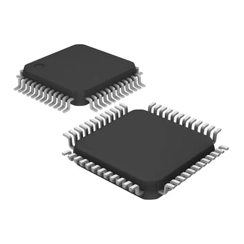
Novatek NT6862-5 Series User manual

NT6862-5xxxx
8-Bit Microcontroller for Monitor
1V2.2
Features
nOperating voltage range: 4.5V to 5.5V
nCMOS technology for low power consumption
n6502 8-bit CMOS CPU core
n8 MHz operation frequency
n32K/24K/16K bytes of ROM
n512 bytes of RAM
nOne 8-bit base timer
n13 channels of 8-bit PWM outputs with 5V open drain
n4 channel A/D converters with 6-bit resolution
n25 bi-directional I/O port pins (8 dedicated I/O pins)
nHsync/Vsync signals processor for separate &
composite signals which includes hardware sync
signals polarity detection and frequency counters with
2 sets of Hsync counting intervals
nHsync/Vsync polarity controlled output, 5 selectable
free run output signals and self-test patterns, auto-
mute function, half freq. I/O function
nAdd a jitter filter at the front end of Hsync input path,
reduce the jitter interference of Hysync input
nTwo built-in I
2C bus interfaces support VESA
DDC1/2B+
nTwo layers of interrupt management
NMI interrupt sources
- INTE0 (External INT with selectable edge trigger)
- INTMUTE (Auto Mute Activated)
IRQ interrupt sources
- INTS0/1 (SCL Go-low INT)
- INTA0/1 (Slave Address Matched INT)
- INTTX0/1 (Shift Register INT)
- INTRX0/1 (Shift Register INT)
- INTNAK0/1 (No Acknowledge)
- INTSTOP0/1 (Stop Condition Occurred INT)
- INTE1 (External INT with Selectable Edge Trigger)
- INTV (VSYNC INT)
- INTMR (Base Timer INT)
- INTADC (AD Conversion Done INT)
nHardware Watch-dog timer function
n40-pin P-DIP and 42-pin S-DIP packages
General Description
The NT6862 is a new generation monitor µC for auto-sync
and digital control applications. Particularly, this chip
supports various and efficient functions to allow users to
easily develop USB monitors. It contains the 6502 8-bit
CPU core, 512 bytes of RAM used as working RAM and
stack area, 32K bytes of OTP ROM, 13-channels of 8-bit
PWM D/A converters, 4-channel A/D converters for key
detection which save I/O pins, one 8-bit pre-loadable base
timer, internal Hsync and Vsync signals processor, a
Watch-dog timer which prevents the system from abnormal
operation, and two I2C bus interfaces. The user can store
EDID data in the 128 bytes of RAM for DDC1/2B, so that
user can reduce a dedicated EEPROM for EDID. A Half
frequency output function can save external one-shot
circuit. These designs are committed to reduce component
cost. The 42 pin S-DIP IC provides two additional I/O pins –
port40 & port41, Part number NT6862U represents the S-
DIP IC. For future reference, port40 & port42 are only
available for the 42 pin S-DIP IC.
NT6862-5xxxx
2
Pin Configurations
40-Pin P-DIP
[PGM] DAC2
DAC1/ADC3
[OE] DAC0/ADC2
[DB7] P27
[VPP] RESET
V
DD
GND
OSCO
OSCI
[CE] P14/PATTERN
[A10] P12/HALFO
[A9] P11/ADC1
[A8] P10/ADC0
P20 [DB0]
P07/HSYNCO [A7]
P31/SCL0 [A13]
DAC4/SCL1 [MODE1]
DAC3 [MODE0]
HSYNCI
VSYNCI/INTV [A14]
NT6862
1
2
3
4
5
6
7
8
9
10
11
12
13
14
15
16 25
26
27
28
29
30
31
32
33
34
35
36
37
38
39
40
P15/INTE0
[A11] P13/HALFI
P16/INTE1
17
18
19
20
24
23
22
21
DAC5/SDA1 [MODE2]
DAC6 [RESET]
CREG
P21 [DB1]
P22 [DB2]
P06/VSYNCO [A6]
P05/DAC12 [A5]
P04/DAC11 [A4]
P03/DAC10 [A3]
P02/DAC9 [A2]
P01/DAC8 [A1]
P00/DAC7 [A0]
P30/SDA0 [A12]
[DB6] P26
[DB5] P25
[DB4] P24
[DB3] P23
* [ ]: OTP Mode
42-Pin S-DIP
[PGM] DAC2
DAC1/ADC3
[OE] DAC0/ADC2
[VPP] RESET
V
DD
P40
GND
OSCO
OSCI
P15/INTE0
[A11] P13/HALFI
[A9] P11/ADC1
[A8] P10/ADC0 P00/DAC7 [A0]P16/INTE1 P01/DAC8 [A1]
P02/DAC9 [A2]
P03/DAC10 [A3]
P04/DAC11 [A4]
P06/VSYNCO [A6]
P07/HSYNCO [A7]
DAC6 [RESET]
P41
DAC5/SDA1 [MODE2]
DAC4/SCL1 [MODE1]
DAC3 [MODE0]
HSYNCI
VSYNCI/INTV [A14]
CREG
NT6862U
1
2
3
4
5
6
7
8
9
10
11
12
13
14
15
16 27
28
29
30
31
32
33
34
35
36
37
38
39
40
41
42
[CE] P14/PATTERN
[A10] P12/HALFO
[DB7] P27
[DB6] P26
[DB5] P25
[DB4] P24
[DB3] P23
17
18
19
20
21
P05/DAC12 [A5]
P31/SCL0 [A13]
P30/SDA0 [A12]
P20 [DB0]
P21 [DB1]
P22 [DB2]
26
25
24
23
22
* [ ]: OTP Mode
Block Diagram
Timing Generator
CPU core
6502
Interrupt
Controller
H/V Sync Signals
Processor
SRAM + STACK
512 Bytes
Watch Dog Timer
PWM DACs
I/O Ports
OSCI
OSCO
VDD
GND
HSYNCI
INTE0/1
SCL0
SDA0
DAC0 - DAC7
P00 - P07
P10 - P16
P30 - P31
VSYNCO
A/D Converter ADC0 - ADC3
8-Bit Base Timer
P40 - P41
IIC BUS
P20 - P27
HSYNCO
HALFI
HALFO
DAC8 - DAC12
VSYNCI/INTV
OTP Program ROM
32K Bytes
PATTERN
SCL1
SDA1
Voltage
Regulator
CREG

NT6862-5xxxx
3
Pin Description
Pin No.
40 Pin 42 Pin Designation Reset Init. I/O Description
1 1 DAC2
[PGM ]
O
[ I ]
Open drain 5V, D/A converter output 2
[OTP ROM program control]
2 2 DAC1/ADC3 DAC1 OOpen drain 5V, D/A converter output 1, shared with A/D
converter channel 3 input
3 3 DAC0/ADC2
[OE ]
DAC0 OOpen drain 5V, D/A converter output 0, shared with A/D
converter channel 2 input
[OTP ROM program output enable]
4 4 RESET
[ VPP ]
I
[ P ]
Schmitt Trigger input pin, low active reset with internal
pulled down 50KΩregister *
[OTP ROM program supply voltage]
5 5 VDD PPower
6 7 GND PGround
7 8 OSCO OCrystal OSC output
8 9 OSCI ICrystal OSC input
9 10 P15/INTE0 I/O Bi-directional I/O pin with internally pulled up 22KΩ
register, shared with input pin of external interrupt source0
(NMI), with Schmitt Trigger, selectable triggered, and
internally pulled up 22KΩregister
10 11 P14/PATTERN
[ A15/CE ]
I/O
[ I ]
Bi-directional I/O pin with internally pulled up 22KΩ
register, shared with the output of self test pattern
[ OTP ROM program address buffer & chip enable ]
11 12 P13/HALFI
[ A11 ]
P13 I/O
[ I ]
Bi-directional I/O pin with internally pulled up 22KΩ
register, shared with half Hsync input.
[ OTPROM program address buffer ]
12 13 P12/HALFO
[ A10 ]
P12 I/O
[ I ]
Bi-directional I/O pin with internally pulled up 22KΩ
register, shared with half Hsync output
[ OTPROM program address buffer ]
13 14 P11/ADC1
[ A9 ]
P11 I/O
[ I ]
Bi-directional I/O pin with internally pulled up 22KΩregister,
shared with A/D converter channel 1 input
[ OTPROM program address buffer ]
14 15 P10/ADC0
[ A8 ]
P10 I/O
[ I ]
Bi-directional I/O pin with internally pulled up 22KΩregister,
shared with A/D converter channel 0 input
[ OTPROM program address buffer ]
15 16 P16/INTE1 P16 I/O Bi-directional I/O pin with internally pulled up 22KΩregister,
shared with input pin of external interrupt source1, with
Schmitt Trigger, selectable triggered, and an internal pulled
up 22KΩregister

NT6862-5xxxx
4
Pin Description (continued)
Pin No.
40 Pin 42 Pin Designation Reset Init. I/O Description
16 - 23 17 - 24 P27 –P20
[ DB7] –[ DB0]
I/O
[ I/O ]
Bi-directional I/O pin, push-pull structure with high current
drive/sink capability
[ OTP ROM program data buffer ]
24 25 P30/SDA0
[ A12 ]
P30 I/O
[ I ]
Open drain 5V bi-directional I/O pin P30, shared with
SDA0 pin of I2C bus Schmitt Trigger buffer
[ OTPROM program address buffer ]
25 26 P31/SCL0
[ A13 ]
P31 I/O
[ I ]
Open drain 5V bi-directional I/O pin P31, shared with
SCL0 pin of I2c bus Schmitt Trigger buffer
[ OTPROM program address buffer ]
26 27 P00/DAC7
[ A0 ]
P00 I/O
[ I ]
Bi-directional I/O pin with internally pulled up 22KΩ
register, shared with open drain 5V D/A converter output
8
[ OTPROM program address buffer ]
27 28 P01/DAC8
[ A1 ]
P01 I/O
[ I ]
Bi-directional I/O pin withinternallypulled up 22KΩ
register, shared with open drain 5V D/A converter output
9
[ OTPROM program address buffer ]
28 29 P02/DAC9
[ A2 ]
P02 I/O
[ I ]
Bi-directional I/O pin withinternallypulled up 22KΩ
register, shared with open drain 5V D/A converter output
10
[ OTPROM program address buffer ]
29 30 P03/DAC10
[ A3 ]
P03 I/O
[ I ]
Bi-directional I/O pin withinternallypulled up 22KΩ
register, shared with open drain 5V D/A converter output
11
[ OTPROM program address buffer ]
30 31 P04/DAC11
[ A4 ]
P04 I/O
[ I ]
Bi-directional I/O pin withinternallypulled up 22KΩ
register, shared with open drain 5V D/A converter output
12
[ OTPROM program address buffer ]
31 32 P05/DAC12
[ A5 ]
P05 I/O
[ I ]
Bi-directional I/O pin withinternallypulled up 22KΩ
register, shared with open drain 5V D/A converter output
13
[ OTPROM program address buffer ]
32 33 P06/VSYNCO
[ A6 ]
P06 I/O
[ I ]
Bi-directional I/O pin withinternallypulled up 22KΩ
register, shared with vsync out
[ OTPROM program address buffer ]
33 34 P07/HSYNCO
[ A7 ]
P07 I/O
[ I ]
Bi-directional I/O pin withinternallypulled up 22KΩ
register, shared with hsync out
[ OTPROM program address buffer ]
34 35 CREG OOn chip voltage regulator output. [Connect external
regulating cap. (10µF - 100µF) here]
35 36 DAC6
[RESET]O
[ I ] Open drain 5V, D/A converter output 6
[ OTPROM reset ]

NT6862-5xxxx
5
Pin Description (continued)
Pin No. Designation Reset Init. I/O Description
40 Pin 42 Pin
36 38 DAC5/SDA1
[ MODE2 ]
O
[ I ]
Open drain 5V, D/A converter output 5, shared with open
drain SDA1 line of I2C bus, Schmitt Trigger buffer
[ OTPROM modeselect]
37 39 DAC4/SCL1
[ MODE1 ]
O
[ I ]
Open drain 5V, D/A converter output 4, shared with open
drain SCL1 line of I2C bus, Schmitt Trigger buffer
[ OTPROM modeselect]
38 40 DAC3
[ MODE0 ]
O
[ I ]
Open drain 5V, D/A converter output 3
[ OTPROM modeselect]
39 41 HSYNCI IDebouncing & Schmitt Trigger input pin for video
horizontal sync signal internally pulled high, shared with
composite sync input. A jitter filter is added at the front
end, it could effectually reduce the jitter interference of
external noisy Hsync input.
40 42 VSYNCI/INTV
[ A14 ]
VSYNCI I
[ I ]
Debouncing & Schmitt Trigger input pin for video vertical
sync signal, internal pull high, shared with input pin of
external interrupt source intv with Schmitt Trigger,
selectable triggered, and internal pulled up 22KΩregister
[ OTPROM program address buffer ]
-6P40 I/O Bi-directional I/O pin with internal pulled up 22KΩ
register, only 42 pinS-DIP available
-37 P41 I/O Bi-directional I/O pin with internal pulled up 22KΩ
register, only 42 pinS-DIP available
*This RESET pin must be pulled high by an external pulled-up register (5KΩsuggestion), or it will remain in low voltage
and continually keep the system in a rest state..

NT6862-5xxxx
6
Functional Description
1. 6502 CPU
The 6502 is an 8-bit CPU that provides 56 instructions, decimal and binary arithmetic, thirteen addressing modes, true
indexing capability, programmable stack pointer and variable length stack, a wide selection of addressable memory ranges,
and interrupt input options.
The CPU clock cycle is 4MHz (8MHz system clock divided by 2). Please refer to the 6502 data sheet for more detailed
information.
Accumulator A
Index Register Y
07
7
Index Register X
7 0
0
Stack Pointer SP 0
Status Register P
07
Carry
Zero
IRQ Disable
Decimal Mode
BRK Command
Overflow
Negative
Figure 1.1. The 6502 CPU Registers and Status Flags
7
Program Counter PCH 815
7 0
PCL
1=TRUE
1=Result ZERO
1=DISABLE
1=TRUE
1=NEG
1=TRUE
1=BRK
NVC
ZID
B

NT6862-5xxxx
7
2. Instruction Set List
Instruction Code Meaning Operation
ADC Add with carry A + M + C→A, C
AND Logical AND A•M →A
ASL Shift left one bit C ←M7 …M0 ←0
BCC Branch if carry clears Branch on C=0
BCS Branch if carry sets Branch on C=1
BEQ Branch if equal to zero Branch on Z =1
BIT Bit test A•M, M7→N, M6→V
BMI Branch if minus Branch on N=1
BNE Branch if not equal to zero Branch on Z =0
BPL Branch if plus Branch on N=0
BRK Break Forced Interrupt PC+2↓PC↓
BVC Branch if overflow clears Branch on V =0
BVS Branch if overflow sets Branch on V =1
CLC Clear carry 0 →C
CLD Clear decimal mode 0 →D
CLI Clear interrupt disable bit 0 →I
CLV Clear overflow 0 →V
CMP Compare Accumulator to memory A -M
CPX Compare with index register X X -M
CPY Compare with index register Y Y -M
DEC Decrement memory by one M -1→M
DEX Decrement index X by one X -1→X
DEY Decrement index Y by one Y -1→Y
EOR Logical exclusive-OR A ⊕M→A
INC Increment memory by one M + 1→M
INX Increment index X by one X + 1→X
INY Increment index Y by one Y + 1→Y

NT6862-5xxxx
8
Instruction Set List (continued)
Instruction Code Meaning Operation
JMP Jump to new location (PC+1)→PCL, (PC+2)→PCH
JSR Jump to subroutine PC+2↓, (PC+1)→PCL, (PC+2)→PCH
LDA Load accumulator with memory M →A
LDX Load index register X with memory M →X
LDY Load index register Y with memory M →Y
LSR Shift right one bit 0 →M7 …M0 →C
NOP No operation No operation (2 cycles)
ORA Logical OR A + M →A
PHA Push accumulator on stack A ↓
PHP Push status register on stack P ↓
PLA Pull accumulator from stack A ↑
PLP Pullstatusregisterfromstack P ↑
ROL Rotate left through carry C ←M7 …M0 ←C
ROR Rotate right through carry C →M7 …M0 →C
RTI Return from interrupt P ↑, PC↑
RTS Return from subroutine PC ↑, PC+1→PC
SBC Subtract with borrow A -M -C→A, C
SEC Set carry 1 →C
SED Setdecimalmode 1 →D
SEI Set interrupt disable status 1 →I
STA Store accumulator in memory A →M
STX Store index register X in memory X →M
STY Store index register Y in memory Y →M
TAX Transfer accumulator to index X A →X
TAY Transfer accumulator to index Y A →Y
TSX Transfer stack pointer to index X S →X
TXA Transfer index X to accumulator X →A
TXS Transfer index X to stack pointer X →S
TYA Transfer index Y to accumulator Y →A
* Refer to 6502 programming data book for more details.

NT6862-5xxxx
9
3. RAM: 512 X
8 bits
The built-in 512X8-bit SRAM is used for data memory and stack area. The RAM addressing range is from $0080 to $027F.
The contents of RAM are undetermined at power-up and are not affected by system reset. Software programmers can
allocate stack area in the RAM by setting stack pointer register (S). Because the 6502 default stack pointer is $01FF,
programmers must set S register to FFH when starting the program.
as; LDX #$FF
TXS
RAM
Unused
ROM
$0000
$0080
$8000
$FFFF
stack pointer
$FFFE
$FFFD
$FFFC RST-L
RST-H
IRQ-L
IRQ-H
RESET vector
IRQ vector
$027F
$0280
( 32 K Bytes )
$003D System Registers
Unused
$7FFF
( 512 Bytes )
$FFFB
$FFFA NMI-L
NMI-H NMI vector
$01FF
4. ROM: 32K X
8bits
NT6862 provides maximum 32K ROM space for code. The ROM space is located from $8000 to $FFFF.
The addresses, from $FFFA to $FFFF, are reserved for the 6502 CPU vectors, thus users must arrange them sepately.

NT6862-5xxxx
10
5. System Registers
Addr. Register INIT Bit7 Bit6 Bit5 Bit4 Bit3 Bit2 Bit1 Bit0 R/W
Control Registers for I/O Port0 & Port1
$0000 PT0 FFH P07 P06 P05 P04 P03 P02 P01 P00 RW
$0001 PT1 7FH -P16 P15 P14 P13 P12 P11 P10 RW
Control Register to Control Port2 I/O Direction
$0002 PT2DIR FFH P27OE P26OE P25OE P24OE P23OE P22OE P21OE P20OE W
Control Registers for I/O Port2 - 4
$0003 PT2 FFH P27 P26 P25 P24 P23 P22 P21 P20 RW
$0004 PT3 03H - - - - - - P31 P30 RW
$0005 PT4 03H Only available for the 42 Pin SDIP version -P41 P40 RW
Control Registers for Synprocessor
FFH - - - -
INSEN
-HSEL S/CR$0006 SYNCON
FFH - - - -
INSEN
ENHSEL HSEL S/CW
FFH - - HSYNCI VSYNCI HPOLI VPOLI HPOLO VPOLO R$0007 HV CON
FFH
ENHOUT
ENHOUT
- - - - HPOLO VPOLO W
$0008 HCNT L 00H HCL7 HCL6 HCL5 HCL4 HCL3 HCL2 HCL1 HCL0 R
HCNTOV - - - HCH3 HCH2 HCH1 HCH0 R$0009 HCNT H 00H
CLRHOV - - - - - - - W
$000A VCNT L 00H VCL7 VCL6 VCL5 VCL4 VCL3 VCL2 VCL1 VCL0 R
VCNTOV -VCH5 VCH4 VCH3 VCH2 VCH1 VCH0 R$000B VCNT H 00H
CLRVOV - - - - - - - W
$000C FREECON FFH ENPAT PAT1 - - - FREQ2 FREQ1 FREQ0 W
$000D HALFCON FFH ENHALF NOHALF HALFPOL - - - - - W
$000E AUTOMUTE FFH
ENHDIFF
ENPOL ENOVER -HDIFFVL3 HDIFFVL2 HDIFFVL1 HDIFFVL0 W
Control Registers to Enable PWM 7 - 12 Channels
$000F ENDAC FFH - - ENDK12 ENDK11 ENDK10 ENDK9 ENDK8 ENDK7 W
Control Registers for ADC 0 - 3 Channels
$0010 ENADC FFH CSTA - - - ENADC3 ENADC2 ENADC1 ENADC0 W
$0011 AD0 REG C0H - - AD05 AD04 AD03 AD02 AD01 AD00 R
$0012 AD1 REG 00H - - AD15 AD14 AD13 AD12 AD11 AD10 R
$0013 AD2 REG 00H - - AD25 AD24 AD23 AD22 AD21 AD20 R
$0014 AD3 REG 00H - - AD35 AD34 AD33 AD32 AD31 AD30 R

NT6862-5xxxx
11
System Registers (continued)
Addr. Register INIT Bit7 Bit6 Bit5 Bit4 Bit3 Bit2 Bit1 Bit0 R/W
Control Register for Polling (Read) Interrupt Groups & Clearing (Write) INTE0 & INTMUTE Interrupt Requests
- - - - - - INTE0 INTMUTE R$0016 NMIPOLL 00H
- - - - - - CLRE0 CLRMUTE W
$0017 IRQPOLL 00H - - - - - IRQ2 IRQ1 IRQ0 R
Control Registers of Interrupt Enable
$0018 IENMI 00H - - - - - - INTE0 INTMUTE RW
$0019 IEIRQ0 00H - - INTS0 INTA0 INTTX0 INTRX0 INTNAK0 INTSTOP0 RW
$001A IEIRQ1 00H - - INTS1 INTA1 INTTX1 INTRX1 INTNAK1 INTSTOP1 RW
$001B IEIRQ2 00H - - - - INTADC INTV INTE1 INTMR RW
Control Registers for Polling (Read) & Clearing (Write) Interrupt Requests
- - INTS0 INTA0 INTTX0 INTRX0 INTNAK0 INTSTOP0 R$001C IRQ0 00H
- - CLRS0 CLRA0 CLRTX0 CLRRX0 CLRNAK0 CLRSTOP0 W
- - INTS1 INTA1 INTTX1 INTRX1 INTNAK1 INTSTOP1 R$001D IRQ1 00H
- - CLRS1 CLRA1 CLRTX1 CLRRX1 CLRNAK1 CLRSTOP1 W
- - - - INTADC INTV INTE1 INTMR R$001E IRQ2 00H
- - - - CLRADC CLRV CLRE1 CLRMR W
Selection of Edge Triggered for INTV, INTE0 & 1 Interrupts
$001F TRIGGER FFH - - - - - INTVR INTE1R INTE0R R/W
Control Registers for Clearing Watch Dog Timer
$0020 CLR WDT -0 1 0 1 0 1 0 1 W
Control Register for DDC1/2B+ of Channel 0
$0021 CH0ADDR A0H ADR7 ADR6 ADR5 ADR4 ADR3 ADR2 ADR1 -W
$0022 CH0TXDAT 00H TX7 TX6 TX5 TX4 TX3 TX2 TX1 TX0 W
$0023 CH0RXDAT 00H RX7 RX6 RX5 RX4 RX3 RX2 RX1 RX0 R
E0H ENDDC MD1/ 2-START STOP -TXACK -W$0024 CH0CON
- - SRW START STOP - - - R
$0025 CH0CLK FFH MODE MRW RSTART - - DDC2BR2 DDC2BR1 DDC2BR0 W
Control Register for DDC1/2B+ of Channel 1
$0026 CH1ADDR A0H ADR7 ADR6 ADR5 ADR4 ADR3 ADR2 ADR1 -W
$0027 CH1TXDAT 00H TX7 TX6 TX5 TX4 TX3 TX2 TX1 TX0 W
$0028 CH1RXDAT 00H RX7 RX6 RX5 RX4 RX3 RX2 RX1 RX0 R

NT6862-5xxxx
12
System Registers (continued)
Addr. Register INIT Bit7 Bit6 Bit5 Bit4 Bit3 Bit2 Bit1 Bit0 R/W
ENDDC MD1/ 2-START STOP -TXACK -W$0029 CH1CON E0H
- - SRW START STOP - - - R
$002A CH1CLK FFH MODE MRW RSTART - - DDC2BR2 DDC2BR1 DDC2BR0 W
Control Registers for Base Timer
$002E BT 00H BT7 BT6 BT5 BT4 BT3 BT2 BT1 BT0 W
$002F BTCON 03H - - - - - - BTCLK ENBT W
Control Registers for PWM Channel 0 - 12
$0030 DACH0 80H DKVL7 DKVL6 DKVL5 DKVL4 DKVL3 DKVL2 DKVL1 DKVL0 RW
$0031 DACH1 80H DKVL7 DKVL6 DKVL5 DKVL4 DKVL3 DKVL2 DKVL1 DKVL0 RW
$0032 DACH2 80H DKVL7 DKVL6 DKVL5 DKVL4 DKVL3 DKVL2 DKVL1 DKVL0 RW
$0033 DACH3 80H DKVL7 DKVL6 DKVL5 DKVL4 DKVL3 DKVL2 DKVL1 DKVL0 RW
$0034 DACH4 80H DKVL7 DKVL6 DKVL5 DKVL4 DKVL3 DKVL2 DKVL1 DKVL0 RW
$0035 DACH5 80H DKVL7 DKVL6 DKVL5 DKVL4 DKVL3 DKVL2 DKVL1 DKVL0 RW
$0036 DACH6 80H DKVL7 DKVL6 DKVL5 DKVL4 DKVL3 DKVL2 DKVL1 DKVL0 RW
$0037 - - - - - - - - -
$0038 DACH7 80H DKVL7 DKVL6 DKVL5 DKVL4 DKVL3 DKVL2 DKVL1 DKVL0 RW
$0039 DACH8 80H DKVL7 DKVL6 DKVL5 DKVL4 DKVL3 DKVL2 DKVL1 DKVL0 RW
$003A DACH9 80H DKVL7 DKVL6 DKVL5 DKVL4 DKVL3 DKVL2 DKVL1 DKVL0 RW
$003B DACH10 80H DKVL7 DKVL6 DKVL5 DKVL4 DKVL3 DKVL2 DKVL1 DKVL0 RW
$003C DACH11 80H DKVL7 DKVL6 DKVL5 DKVL4 DKVL3 DKVL2 DKVL1 DKVL0 RW
$003D DACH12 80H DKVL7 DKVL6 DKVL5 DKVL4 DKVL3 DKVL2 DKVL1 DKVL0 RW

NT6862-5xxxx
13
6. Timing Generator
This block generates the system timing and control signal
to be supplied to the CPU and on-chip peripherals. A
crystal quartz, ceramic resonator, or an external clock
signal which will be provided to the OSCI pin generates
system timing. It generates 8MHz system clock, 4MHz for
the CPU. Although internal circuits have a feedback resister
and compacitor included, users can externally add these
components for proper operating.
The typical clock frequency is 8MHz. Different frequencies
will affect the operation of those on-chip peripherals whose
operating frequency is based on the system clock.
8MHz OSCI
OSCO
NT68P62
OSCI
NT68P62
Figure 6.1. Oscillator Connections
(1) (2)
Unconnected
External Clock
OSCO
7. RESET
The NT6862 can be reset by the external reset pin or by
the internal Watch-dog timer. This is used to reset or start
the microcontroller from a POWER DOWN condition.
During the time that this reset pin is heldLOW, writing to or
from theµC is inhibited. (*The reset line must be held LOW
for at least two CPU clock cycles) When a positive edge is
detected on the RESET input, the µC will immediately
begin the reset sequence.
After a system initialization time of six CPU clock cycles,
the mask interrupt flag will be set and the µC will load the
program counter from the memory vector locations $FFFC
and $FFFD. This is the start location for program control.
An internal Schmitt Trigger buffer at the RESET pin is
provided to improve noise immunity.
The reset status is as follows:
1. PORT0、PORT1、PORT2、PORT3 (& PORT4) pins
will act as I/O ports with HIGH output
2. Sync processor counters reset and VCNT | HCNT
latches cleared
3. All sync outputs are disabled
4. Base timer is disabled and cleared
5. Various Interrupt sources are disabled and cleared
6. A/D converter is disabled and stopped
7. DDC1/2B+ function is disabled
8. PWM DAC0 –DAC6 output 50% duty waveform and
DAC7 - DAC12 is disabled
9. Watch-dog timer is cleared and enabled

NT6862-5xxxx
14
8. A/D Converters
The structure of these analog to digital converters is 6-bit
successive approximation. Analog voltage is supplied from
external sources to the A/D input pins and the result of the
conversion is stored in the 6-bit data latch registers ($0011
& $0014). The A/D channels are activated by clearing the
correspondent control bits in the ENADC control register.
When users write '0' to one of the enable control bits, its
correspondent I/O pin or DAC will be switched to the A/D
converter input pin (ADC0 & ADC1 shared with PORT10 &
PORT 11; ADC2 & ADC3 shared wit DAC0 & DAC1).
Conversion will be started by clearing CSTA bit
(CONVERSION START) in the ENADC control register.
When conversion is finished, system will set this INTADC
bit. Users can monitor this bit to get the valid A/D
conversion data in the AD latch registers ($0011 - $0014).
Users can also open interrupt sources to remind users to
get the stable digital data. Note that latched data is only
available at the activated A/D channel.
The analog voltage to be measured should be stabled
during the conversion operation and the variation will not
exceed LSB for the best accuracy in measurement.
Addr. Register INIT Bit7 Bit6 Bit5 Bit4 Bit3 Bit2 Bit1 Bit0 R/W
$0010 ENADC FFH CSTA ---ENADC3 ENADC2 ENADC1 ENADC0 W
$0011 AD0 REG C0H - - AD05 AD04 AD03 AD02 AD01 AD00 R
$0012 AD1 REG 00H - - AD15 AD14 AD13 AD12 AD11 AD10 R
$0013 AD2 REG 00H - - AD25 AD24 AD23 AD22 AD21 AD20 R
$0014 AD3 REG 00H - - AD35 AD34 AD33 AD32 AD31 AD30 R
$001B IEIRQ2 00H ----INTADC INTV INTE1 INTMR R/W
$001E IRQ2 00H ----INTADC INTV INTE1 INTMR R
----CLRADC CLRV CLRE1 CLRMR W
Reference ADC Table (VDD = 5.0V)
15 1.53V 1C 2.07V 23 2.62V 2A 3.16V
16 1.62V 1D 2.16V 24 2.70V 2B 3.25V
17 1.69V 1E 2.23V 25 2.77V 2C 3.33V
18 1.76V 1F 2.31V 26 2.85V 2D 3.40V
19 1.84V 20 2.39V 27 2.93V 2E 3.48V
1A 1.92V 21 2.47V 28 3.01V 2F 3.56V
1B 2.00V 22 2.54V 29 3.09V 30 3.64V
Note: It is strongly recommended that the ADC’s input signal should be allocated in the ADC’s linear voltage range
(1.5V - 3.5V) to obtain a stable digital value. Do not use the outer ranges (0V - 1.4V & 3.6V - 5.0V) in which the
converted digital value is not guaranteed.

NT6862-5xxxx
15
9. PWM DACs (Pulse Width Modulation D/A Converters)
There are 13 PWM D/A converters with 8-bit resolution in NT6862. All of these D/A (DAC0 - DAC12) converters are open-
drain output structure with an external 5V applied maximum. DAC0 –DAC6 are dedicated PWM channels, and DAC7 -
DAC12 are shared with I/O pins. Those shared PWM channels are activated by clearing the correspondent control bits in the
ENDAC control register ($000F). When users write '0' into one of the enable control bits, its correspondent I/O pin will be
switched to PWM output pin.
The PWM refresh rate is 62.5KHz operating on 8MHz system clock. There are 13 readable DACH registers corresponding to
13 PWM channels ($0030 - $003D). Each PWM output pulse width is programmable by setting the 8 bit digital to the
corresponding DACH registers. When these DACH registers are set to 00H, the DAC will output LOW (GND level) and every
1 bit addition will add 62.5ns pulse width. After reset, all DAC outputs are set to80H (1/2 duty output). Please refer to Figure
9.1 for the detailed timing diagram of PWM D/A output.
01
02
m
255(FF)
Fosc
255 0 1 2 m255 1PWM value :
8MHz
00
Figure 9.1. The DAC Output Timing Diagram and Wave Table
03
3m-1 0

NT6862-5xxxx
16
PWM DACs (continued)
DAC0 & DAC1 are shared with ADC2 & ADC3 input pins respectively. If ENADC2/3bit in the ENADC control register is
cleared to LOW, A/D converters will activate simultaneously. After the chip is reset, ENADC2/3bits will be in HIGH state
and DAC0 & DAC1 will act as PWM output pins.
DAC4 & DAC5 are shared with SCL1 & SDA1 I/O pins respectively. If users clear the ENDDC bit in the CH1CON control
register to LOW, channel 1 of DDC will be activated. When used as DDC channel, the I/O port will be an open drain structure
and include a Schmitt Trigger buffer for noise immunity. After the chip is reset, ENDDC bits will be in HIGH state and DAC4
- DAC5 will act as PWM output pins.
Addr. Register INIT Bit7 Bit6 Bit5 Bit4 Bit3 Bit2 Bit1 Bit0 R/W
$000F ENDAC FFH - - ENDK12 ENDK11 ENDK10 ENDK9 ENDK8
ENDK7
W
$0010 ENADC FFH CSTA - - - ENADC3 ENADC2 ENADC1 ENADC0 W
$0030 DACH0 80H DKVL7 DKVL6 DKVL5 DKVL4 DKVL3 DKVL2 DKVL1 DKVL0 RW
$0031 DACH1 80H DKVL7 DKVL6 DKVL5 DKVL4 DKVL3 DKVL2 DKVL1 DKVL0 RW
$0032 DACH2 80H DKVL7 DKVL6 DKVL5 DKVL4 DKVL3 DKVL2 DKVL1 DKVL0 RW
$0033 DACH3 80H DKVL7 DKVL6 DKVL5 DKVL4 DKVL3 DKVL2 DKVL1 DKVL0 RW
$0034 DACH4 80H DKVL7 DKVL6 DKVL5 DKVL4 DKVL3 DKVL2 DKVL1 DKVL0 RW
$0035 DACH5 80H DKVL7 DKVL6 DKVL5 DKVL4 DKVL3 DKVL2 DKVL1 DKVL0 RW
$0036 DACH6 80H DKVL7 DKVL6 DKVL5 DKVL4 DKVL3 DKVL2 DKVL1 DKVL0 RW
$0037 - - - - - - - - -
$0038 DACH7 80H DKVL7 DKVL6 DKVL5 DKVL4 DKVL3 DKVL2 DKVL1 DKVL0 RW
$0039 DACH8 80H DKVL7 DKVL6 DKVL5 DKVL4 DKVL3 DKVL2 DKVL1 DKVL0 RW
$003A DACH9 80H DKVL7 DKVL6 DKVL5 DKVL4 DKVL3 DKVL2 DKVL1 DKVL0 RW
$003B DACH10 80H DKVL7 DKVL6 DKVL5 DKVL4 DKVL3 DKVL2 DKVL1 DKVL0 RW
$003C DACH11 80H DKVL7 DKVL6 DKVL5 DKVL4 DKVL3 DKVL2 DKVL1 DKVL0 RW
$003D DACH12 80H DKVL7 DKVL6 DKVL5 DKVL4 DKVL3 DKVL2 DKVL1 DKVL0 RW
DAC control register ($000F) and DAC value register ($0030 - $003D)

NT6862-5xxxx
17
10. Watch-Dog Timer (WDT)
The NT6862 implements a Watch-dog timer reset to avoid
system stop or malfunction. The clock of the WDT is from
on-chip RC oscillator which does not require any external
components. Thus, the WDT will run, even if the clock on
the OSCI/OSCO pins of the device have been stopped.
The WDT time interval is about 0.5 second. The WDT must
be cleared within every 0.5 second when the software is in
normal sequence, otherwise the WDT will overflow and
cause a reset. The WDT is cleared and enabled after the
system is reset, and can not be disabled by the software.
Users can clear the WDT by writing 55H to CLRWDT
register ($0020).
as; LDA #$55
STA $0020
Addr. Register INIT Bit7 Bit6 Bit5 Bit4 Bit3 Bit2 Bit1 Bit0 R/W
$0020 CLR WDT -01010101W
11. Interrupt Controller
The system provides two kinds of interrupt sources: NMI &
IRQ. The NMI can not be masked and if enabling NMI
interrupt sources, users can execute the NMI interrupt
vector anytime when sources are activated. The IRQ
interrupts can be masked by executing a CLI instruction or
setting the interrupt mask flag directly in the µC status
register. In process IRQ interrupt, if the interrupt mask flag
is not set, the µC will begin an interrupt sequence. The
program counter and processor status register will be
stored in the stack. The µC will then set the interrupt mask
flag HIGH so that no further interrupts may occur. At the
end of this cycle, the program counter will be loaded from
addresses $FFFE & $FFFF, then transferring program
control to the memory vector located at these addresses.
For NMI interrupt, µC will transfer execution sequence to
the memory vector located at addresses $FFFA & $FFFB.
When manipulating various interrupt sources, NT6862
divides them into two groups for accessing them easily.
One is NMI group and the other is IRQ group.
- The NMI group includes INTE0, INTMUTE.
-The IRQ group includes subgroup of IRQ0, IRQ1,RQ2:
IRQ0: DDC1/2B+ Channel 0 interrupt sources; It
includes INTS0, INTA0, INTTX0, INTRX0,
INTNAK0 and INTSTOP0 interrupts.
IRQ1: DDC1/2B+ Channel 1 interrupt sources; It
includes INTS0, INTA1, INTTX1, INTRX1,
INTNAK1 and INTSTOP1.
IRQ2: It includes INTADC, INTV, INTE1 and INTMR
interruptsources.
The interrupt sources are shown below.
Nonmaskable Interrupt Group:
Interrupt Meaning Action
INTE0 INT External 0 INT It will be activated by the rising edge or falling edge of external interrupt pulse.
The triggered edge can be selected by EDGE0 bit.
INTMUTE Auto Mute It will be activated when the mute condition occurres (Hsync frequency
change). Please refer the synprocessor section for more details.
Maskable Interrupt Group:
Interrupt Meaning Action
INTADC A/D Converion
Done User activates the ADC by clearing the CSTART bit. When AD conversion is
done, this bit will be set.
INTV INT Vsync INT It will be activated as the rising edge of every Vsync pulse.
INTE1 INT External 1 INT It will be activated by the rising edge or falling edge of external interrupt pulse.
The triggered edge can be selected by EDGE1 bit.
INTMR INT Timer INT It will be activated as the rising edge of every when the Base Timer counter
overflows and counting from $FF to $00.

NT6862-5xxxx
18
DDC Channel 0/1 Maskable Interrupt Sources:
Interrupt Meaning Action
INTS INT SCL Go-Low INT In DDC1 mode, it will be activated when the external device proceed a DDC2
communication. This action includes pull the SCL line to ground or send out an
'START' condition directly. System will respond to this action by changing
DDC1 mode to DDC2 SLAVE mode.
INTA INT Address Matched
INT It will be activated at DDC2 slave mode when the externaldevice call NT6862
slave address. If this calling address matches the NT6862 address, system will
generate this interrupt to remind user
INTTX INT Transfer Buffer
Empty INT It will be activated at DDC2 mode when transmission buffer, IIC_TXDAT, is
empty at TRAMISSION mode.
INTRX INT Receiving Buffer
Overflow INT It will be activated at DDC2 mode when new data have store in the
IIC_RXDAT register at RECEIVE mode.
INTNAK INT No Acknowledge
INT At transmission mode, this interrupt will be activated when NT6862 have send
out one byte data but the external device does not respond an acknowledge bit
to it.
INTSTOP INT DDC2 Stop INT In SLAVE mode, this interrupt will be activated when the NT6862 receives an
'STOP' condition.
INTSTOP0
INTNAK0
INTRX0
INTTX0
INTA0
INTS0
INTSTOP1
INTNAK1
INTRX1
INTTX1
INTA1
INTS1
INTMR
INTE1
INTV
INTADC
INTMUTE
INTE0
IRQ0
IRQ (to CPU 6502)
NMI (to CPU 6502)
IRQ0
IRQ1
IRQ2
Figure 11.1. Interrupt Controller Structure
IRQ1
IRQ2
IEIRQ0
IEIRQ1
IEIRQ2
NMIPOLL IENMI

NT6862-5xxxx
19
Enabling Interrupts: The system will disable all of these
interrupts after reset. Users can enable each of the
interrupts by setting the interrupt enable bits at IENMI,
IEIRQ0 - IEIRQ3 control registers. For example, if users
want to enable external interrupt 0 (INTE0), the should
write '1' to INTE0 bit in the IENMI control register. At the
INTE0 pin, whenever NT6862 has detected an interrupt
message, it will generate an interrupt sequence to fetch the
NMI vector. Because these IEX control registers can be
read, users can read back what interrupts he has been
activated. At polling sequence, users need not poll those
unactivated interrupts.
To request interrupts to be set: Regardless whether the
user has set the interrupt enable bits or not, if the interrupt
triggered condition is matched, the system will set the
correspondent bits in the IRQ0 - IRQ3 control registers or in
the NMIPOLL control register (INTE0 & INTMUTE bits). For
example, if at VSYNCI pin, the system have detected a
pulse occurring, system will set the INTV bit in the IRQ2
control register.
Interrupt Groups: System divides IRQ interrupt sources into
several groups, ex IRQ0, IRQ1, IRQ2 and IRQ3. At each of
these groups, if its membership in the one of the interrupt
groups have been activated, its group bit in the IRQPOLL
control register will be set. For example, if the INTS0 of the
first DDC1/2B+ channel is activated, the INTS0 bit in the
IRQ0 will be set and the IRQ0 bit in the IRQPOLL control
register also will be set. Notice that the IRQ0 bit will be
cleared by system when all of its membership of interrupt
sources, INTS0, INTTX0, INTRX0, INTNAK0 and
INTSTOP0 have been cleared by the user or system. The
NMI group is also oprating the same procedure as IRQ
groups.
Polling Interrupts: When NMI interrupt occurrs, at NMI
interrupt service routine, users must poll the INTE0 &
INTMUTE bit in the NMIPOLL control register to confirm the
NMI interrupt source. The polling sequence decides the
priority of NMI interrupt acceptation. When IRQ interrupt
occurrs, at IRQ interrupt service routine, users must poll the
IRQ0 - IRQ3 in the IRQPOLL control register to confirm the
IRQ interrupt source. In the same way, the polling
sequence decides the priority of IRQ interrupt acception.
When deciding the IRQ source, users can further confirm
the real interrupt source by polling the Correspondent IRQX
control register ($001C - $001E).
Clearing the Interrupt Request bit: When interrupt occurrs,
the CPU will jump to the address defined by the interrupt
vector to execute interrupt service routine. Users can check
which one of the interrupt sources is activated and
operating a tast. It is that upon entering the interrupt service
routine, the request bit that caused the interrupt must be
cleared by user before finishing the service routine and
returning to normal instruction sequence. If users forget to
clear this request bit, after returning to main program, it will
interrupt CPU again because the request bit remains
activated. Simply, users just need write '1' to the polling bits
in the NMIPOLL & IRQX registers ($0016 & $001C -
$001E) to clear those completed interrupt sources.
Selecting interrupt triggered edge: At INTV, INTE0 & INTE1
interrupt sources, these are now edge triggered type.
System provides the selection of rising or falling edge
triggered under user’s control. After reset, the rising edge
triggered are provided and the content is 'FF' in the
TRIGGER control register ($001F). User just clear control
bits in this TRIGGER register and switch these interrupts to
falling edge triggered.

NT6862-5xxxx
20
Control Bit Description
Addr. Register INIT Bit7 Bit6 Bit5 Bit4 Bit3 Bit2 Bit1 Bit0 R/W
Control Register for Polling Interrupt
- - - - - - INTE0 INTMUTE R$0016 NMIPOLL 00H
- - - - - - CLRE0 CLRMUTE W
$0017 IRQPOLL 00H - - - - - IRQ2 IRQ1 IRQ0 R
Control Registers of Interrupt Enable
$0018 IENMI 00H - - - - - - INTE0 INTMUTE RW
$0019 IEIRQ0 00H - - INTS0 INTA0 INTTX0 INTRX0 INTNAK0 INTSTOP0 RW
$001A IEIRQ1 00H - - INTS1 INTA1 INTTX1 INTRX1 INTNAK1 INTSTOP1 RW
$001B IEIRQ2 00H - - - - INTADC INTV INTE1 INTMR RW
Control Registers for Polling (Read) & Clearing (Write) Interrupt Requests
- - INTS0 INTA0 INTTX0 INTRX0 INTNAK0 INTSTOP0 R$001C IRQ0 00H
- - CLRS0 CLRA0 CLRTX0 CLRRX0 CLRNAK0 CLRSTOP0 W
- - INTS1 INTA1 INTTX1 INTRX1 INTNAK1 INTSTOP1 R
- - CLRS1 CLRA1 CLRTX1 CLRRX1 CLRNAK1 CLRSTOP1 W
$001D IRQ1 00H
- - - - CLRADC CLRV CLRE1 CLRMR W
Selection of Edge Triggered for INTE0 & 1 Interrupt
$001F TRIGGER FFH - - - - - INTVR INTE1R INTE0R R/W
Other Novatek Microcontroller manuals
Popular Microcontroller manuals by other brands

onsemi
onsemi RSL10 Series Getting started guide

Texas Instruments
Texas Instruments CC1110 user guide

Itaca Innovation
Itaca Innovation uChip Quick start manual

Nuvoton
Nuvoton NuMicro MS51 Series Technical reference manual

Texas Instruments
Texas Instruments Serial Programming Adapter MSP430 user guide

SONIX
SONIX SN8P2743 Series user manual

Abov
Abov A96G140 user manual

Texas Instruments
Texas Instruments SimpleLink MSP432P4111 user guide

LAPIS Semiconductor
LAPIS Semiconductor ML610Q421 user manual

ARM
ARM KEIL Infineon XMC4500 Relax Lite Board quick start guide

BECKWITH ELECTRIC
BECKWITH ELECTRIC M-2601 Instruction book

STMicroelectronics
STMicroelectronics STM32L151CCT6 manual