3 Development Board Setup
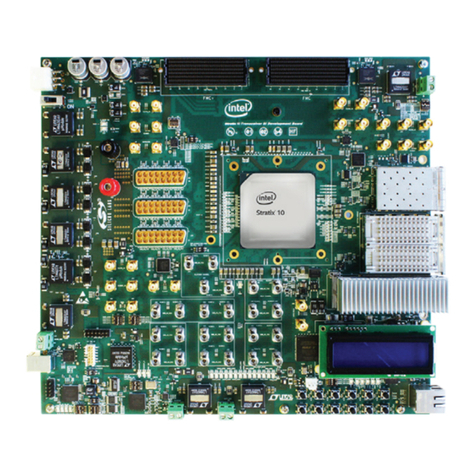
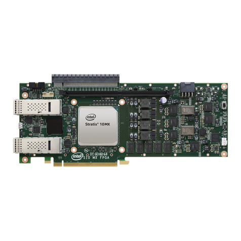
The instructions in this chapter explain how to setup the Intel Stratix 10 GX
Transceiver Signal Integrity Development Board.
3.1 Setting up the Development Board
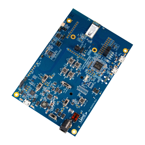
To prepare and apply power to the board, perform the following steps:
1. The Intel Stratix 10 GX transceiver signal integrity development kit ships with its
board switches preconfigured to support the design examples in the kit. If you
suspect your board might not be correctly configured with the default settings,
follow the instructions in the Factory Default Switch and Jumper Settings on page
8 to return the board to its factory settings before proceeding.
2. The development kit ships with design examples stored in the flash device. The
POWER-ON slide switch (SW7) is provided to turn the board ON or OFF.
Caution: When the power cord is plugged into connector J103 of the Intel Stratix
10 transceiver signal integrity development kit, 12V_IN and 3.3V_STBY
are present on to the board with switch SW7 in the 'OFF' position.
These voltages are restricted to a small area of the board. When switch
SW7 is placed to 'ON' position, all voltages planes have power at this
point.
3. Set the POWER-ON switch SW7 to the ON position. When power is supplied to the
board, three green LEDs (D29, D31 and D32) illuminate and an amber LED
(D36) extinguishes indicating that the board has power. If the amber LED (D36)
illuminates, it indicates that one or more power supply is incorrect.
4. RESET button (S12) is connected to the MAX V CPLD (MAX_RESETn pin) that is
used for AvST configuration. When this button is pressed, the MAX V CPLD
initiates a reloading of the stored image from the flash memory using AvST
configuration mode. The image loaded right after power cycle or MAX V reset
depends on FACTORY_LOAD settings.
•OFF(1) - factory load
•ON (0) - user defined load #1
Page selection can be changed by the PGMSEL button (S10) when the board is
powered on, and PGM_CONFIG (S11) is used to reconfigure FPGA with
corresponding page which is indicated by PGM_LED0, PGM_LED1 or PGM_LED2.
Caution: Use only the supplied power supply. Power regulation circuits on the
board can get damaged by power supplies with greater voltage.
The MAX V CPLD device on the board contains a parallel flash loader II (PFL II)
megafunction. After a POWER-ON or RESET (reconfiguration) event, the MAX V CPLD
configures the Intel Stratix 10 FPGA in AvST mode with either factory design or user
design depending on the setting of FACTORY_LOAD.
3 Development Board Setup
Intel Corporation. All rights reserved. Intel, the Intel logo, Altera, Arria, Cyclone, Enpirion, MAX, Nios, Quartus
and Stratix words and logos are trademarks of Intel Corporation or its subsidiaries in the U.S. and/or other
countries. Intel warrants performance of its FPGA and semiconductor products to current specifications in
accordance with Intel's standard warranty, but reserves the right to make changes to any products and services
at any time without notice. Intel assumes no responsibility or liability arising out of the application or use of any
information, product, or service described herein except as expressly agreed to in writing by Intel. Intel
customers are advised to obtain the latest version of device specifications before relying on any published
information and before placing orders for products or services.
*Other names and brands may be claimed as the property of others.
ISO
9001:2008
Registered
