MC1320x RF Daughter Card, Rev. 1.2
8Freescale Semiconductor
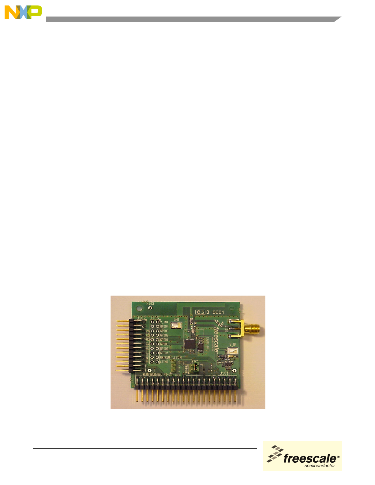
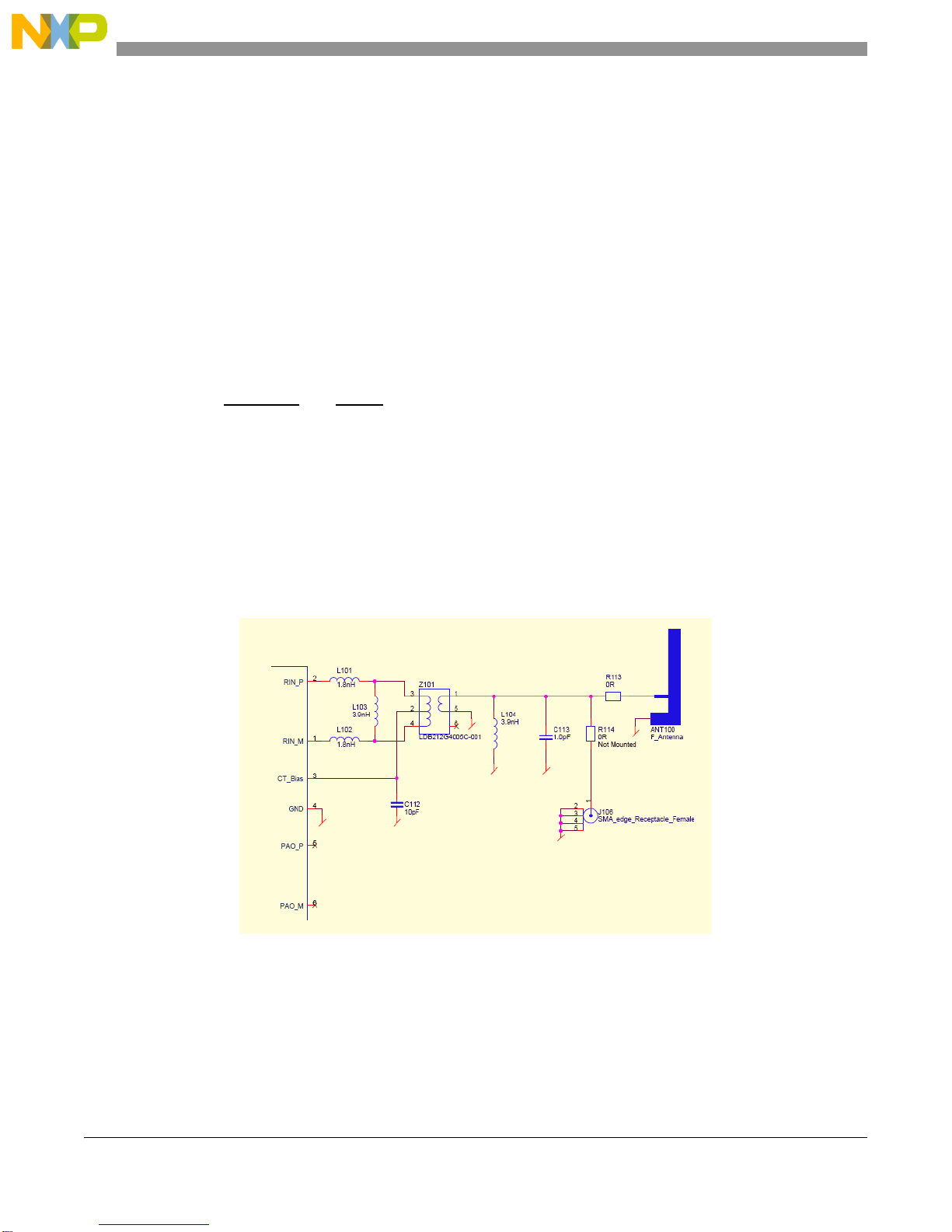
Daughter Card Description
Table 5-2. J102 Pin Connections
Pin Number Pin Names Description Functionality
4, 5, 6, 7, 8, 11, 12, 14,
16, 18, 22 N/C No connection
1 V_IN Connects the Daughter Card to the
supply voltage output on the
M52235EVB.
ProvidessupplyvoltagetotheDaughterCard.
Voltage must not exceed 16 Vdc. See
Section 5.1.0.3, “Power Connections”.
2IRQ
Connects to IRQ pin of MC1320X. Allows the MC1320X to issue an IRQ to the
MCU.
3 GND Connects the ground of the RF
Daughter Card to the ground of the
M52235EVB
9 GPIO1 Connects to General Purpose
Input/Output 1 of MC1320X. When gpio_alt_en, Register 9, Bit 7 = 1,
GPIO1 functions as an “Out of Idle” Indicator.
10 GPOI2 Connects to General Purpose
Input/Output 2 of MC1320X. When gpio_alt_en, Register 9, Bit 7 =1,
GPIO2 functions as a “CRC Valid” Indicator.
13 RESET Connects to RESET of MC1320X
and Pin 32 of J101. Allows the MCU to reset the MC1320X.
15 PTD5/CESI Connects to ATTN of MC1320X
and Pin 34 of J101. Allows the MCU to wake up the MC1320X
from Doze or Hibernate.
17 MOSI Connects to MOSI of MC1320X. SPI
19 MISO Connects to MISO of MC1320X. SPI
20 RXTXEN Connect to RXTXEN of MC1320X. Allows the MCUntrol the RXTXEN line of the
MC1320X.
21 SPICLK Connect to SPICLK of the
MC1320X SPI
23 PTE2/CE-
QSPI-CSO Connects to Pin 1 of J104 Allows Chip Enable (CE) selection.
See Section 5.1.0.1, “SPI Connections”.
24 PTE2/CE-AN7 Connects to Pin 3 of J104 Allows Chip Enable (CE) selection.
See Section 5.1.0.1, “SPI Connections”.