INTRODUCTION:
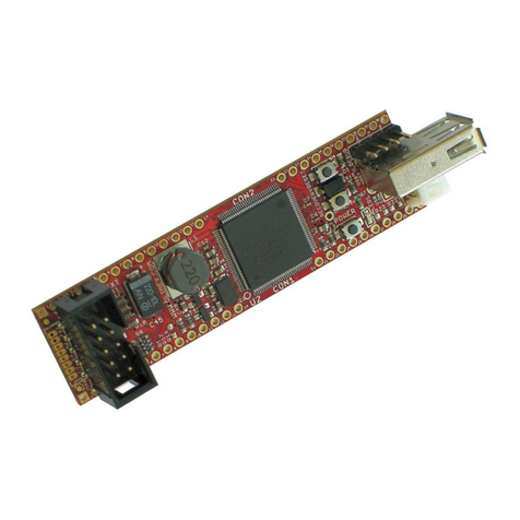
AVR-ISP500-TINY is USB in-system programmer for AVR microcontrollers,
featuring two distincti e methods for communication with PC programming
software.
It can implement the STK500 2 protocol as defined by Atmel which makes
it compatible with a range of tools, including A rStudio and a rdude. It
is distinguished from other programmers by its support for autonomous
operation. AVR-ISP500-TINY contains a 2Mb FLASH memory where it can
store entire programming sessions, including FUSE, LOCK, EEPROM and
FLASH write and erification, as well as signature checking. Just hold the
button, perform all the necessary steps with A rStudio, and disconnect the
programmer from the PC. Next time button is pressed the programmer will
in oke all pre iously recorded steps without the need for connection to the
PC.
The other supported mode is a USB mass storage FLASH dri e where user
can drag and drop HEX files for downloading to target AVR chip.
We belie e these features make AVR-ISP500-TINY the perfect low-cost tool
for firmware upgrades in remote places.
FEATURES:
- Fully STK500 2 compatible;
- Works with A rStudio, WinAVR, A rdude and e ery other software
compatible with STK500 2;
- Two distincti e modes of operation;
- Modes of operation (STK500 2 and Mass Storage Dri e) are switched
easily by uploading firmware images a ailable from our website;
- USB port for connection to PC;
- Stand alone operation without the need for PC connection, allowing
firmware mass programming on many de ices with single button press;
- One bi-color LED for current operation status;
- Supports both standard ICSP10 and ICSP6 connectors;
- Button for initiating autonomous operations and command logging;
- Powered by USB;
- External clock output on ICSP10 pin 3 for rescuing AVRs with enabled
external clock fuse;
- Supports target oltages ranging from 1.8V to 5.5V.
- ISP clock frequencies ranging from 5kHz to 2MHz.
ELECTROSTATIC WARNING:
The AVR-ISP500-TINY board is shipped in protecti e anti-static packaging.
The board must not be subject to high electrostatic potentials. General
practice for working with static sensiti e de ices should be applied when
working with this board.
REQUIREMENTS:
Cables: 1.8 meter USB A-B cable. Ten- or six-wire ribbon cable for
connection to target AVR chip. USB power supply cable for autonomous
operation.

