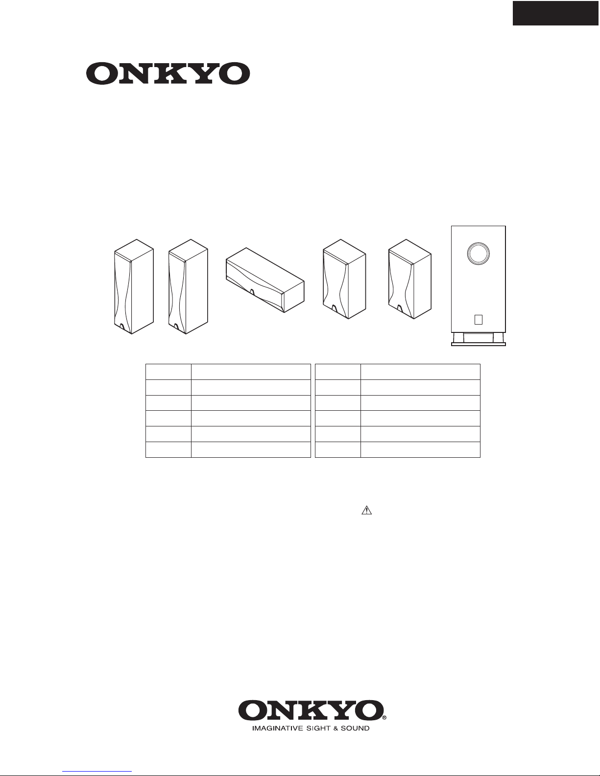
Onkyo HTP-420 User manual

HTP-420
SERVICE MANUAL
SERVICE MANUAL
5.1-CH HOME THEATER SPEAKER PACKAGE
Black and Silver models
MODEL HTP-420(B)/(S)
Ref. No. 3808
042004
120V AC, 60Hz
120V AC, 60Hz
---
230-240V AC, 50Hz
---
---
BMDD
BMDC
---
BMPA
---
---
120V AC, 60Hz
120V AC, 60Hz
120V AC, 60Hz
230-240V AC, 50Hz
220-230V AC, 50/60Hz
230-240V AC, 50Hz
SMDD
SMDC
SMDT
SMPA
SMGT
SMPT
Front Speakers (L / R)
"SKF-420F"
Center Speaker
"SKC-420C"
Surround Speakers (L / R)
"SKM-420S"
Powered Subwoofer
"SKW-420"
SAFETY-RELATED COMPONENT
WARNING!!
COMPONENTS IDENTIFIED BY MARK ON THE
SCHEMATIC DIAGRAM AND IN THE PARTS LIST ARE
CRITICAL FOR RISK OF FIRE AND ELECTRIC SHOCK.
REPLACE THESE COMPONENTS WITH ONKYO
PARTS WHOSE PART NUMBERS APPEAR AS SHOWN
IN THIS MANUAL.
MAKE LEAKAGE-CURRENT OR RESISTANCE
MEASUREMENTS TO DETERMINE THAT EXPOSED
PARTS ARE ACCEPTABLY INSULATED FROM THE
SUPPLY CIRCUIT BEFORE RETURNING THE
APPLIANCE TO THE CUSTOMER.

SPECIFICATIONS
HTP-420
Type :
Input sensitivity/impedance :
Maximum output power :
Frequency response :
Cabinet capacity :
Dimensions (W x H x D) :
Weight :
Driver unit :
Power supply :
America :
Others :
Power consumption :
America :
Australia :
Others :
Other :
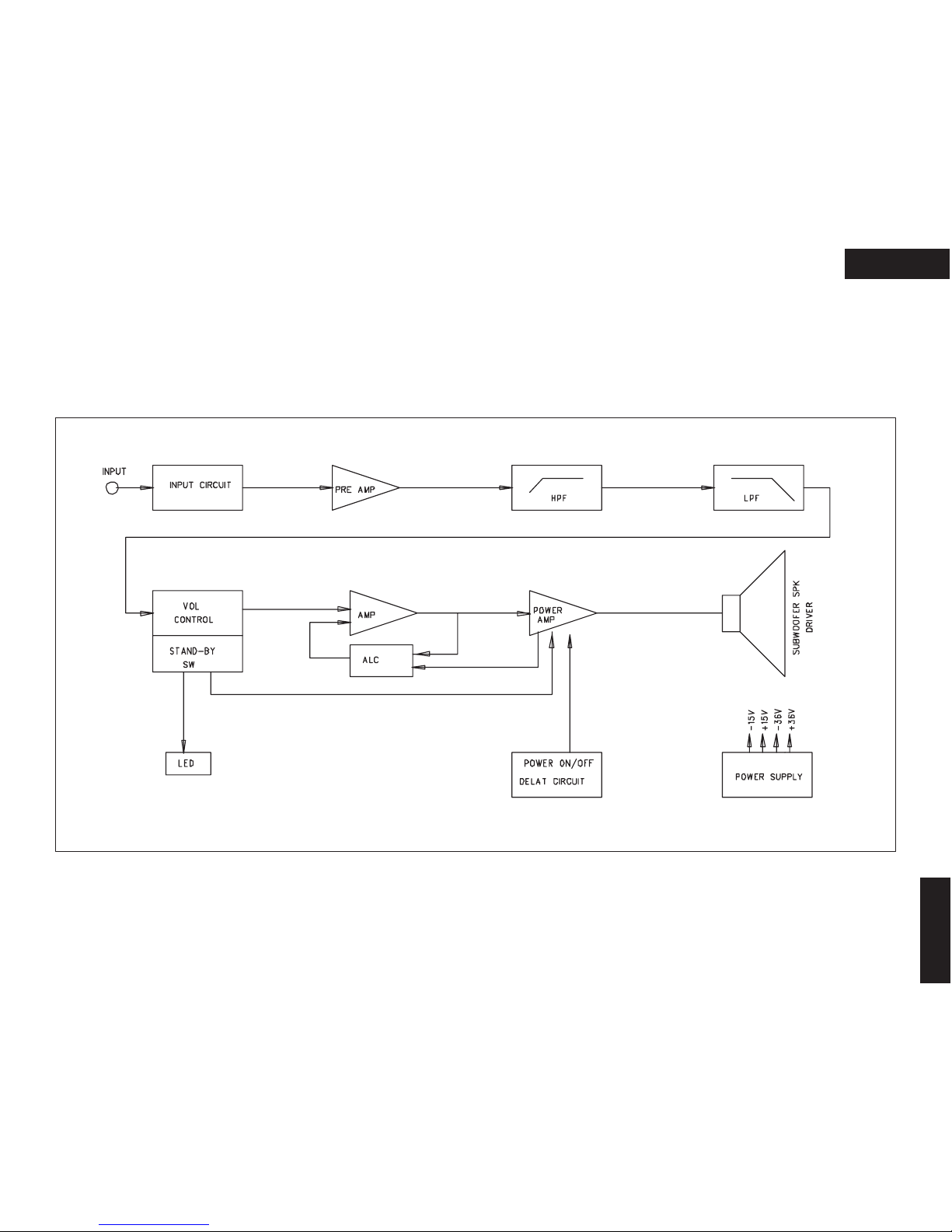
Bass-reflex with built-in
power amplifier
220 mV / 15 k ohm
150 W (Dynamic Power)
30 Hz - 150 Hz
1.15 cubic feet (32.5 L)
9-1/4" x 20-3/8" x 16-3/16"
(235 x 518 x 411 mm)
28.2 lbs. (12.8 kg)
8 inch Cone Woofer
AC 120 V, 60 Hz
AC 230-240 V, 50 Hz
AC 220-230 V, 50/60 Hz
75 W
77 W
77 W
Auto Standby function
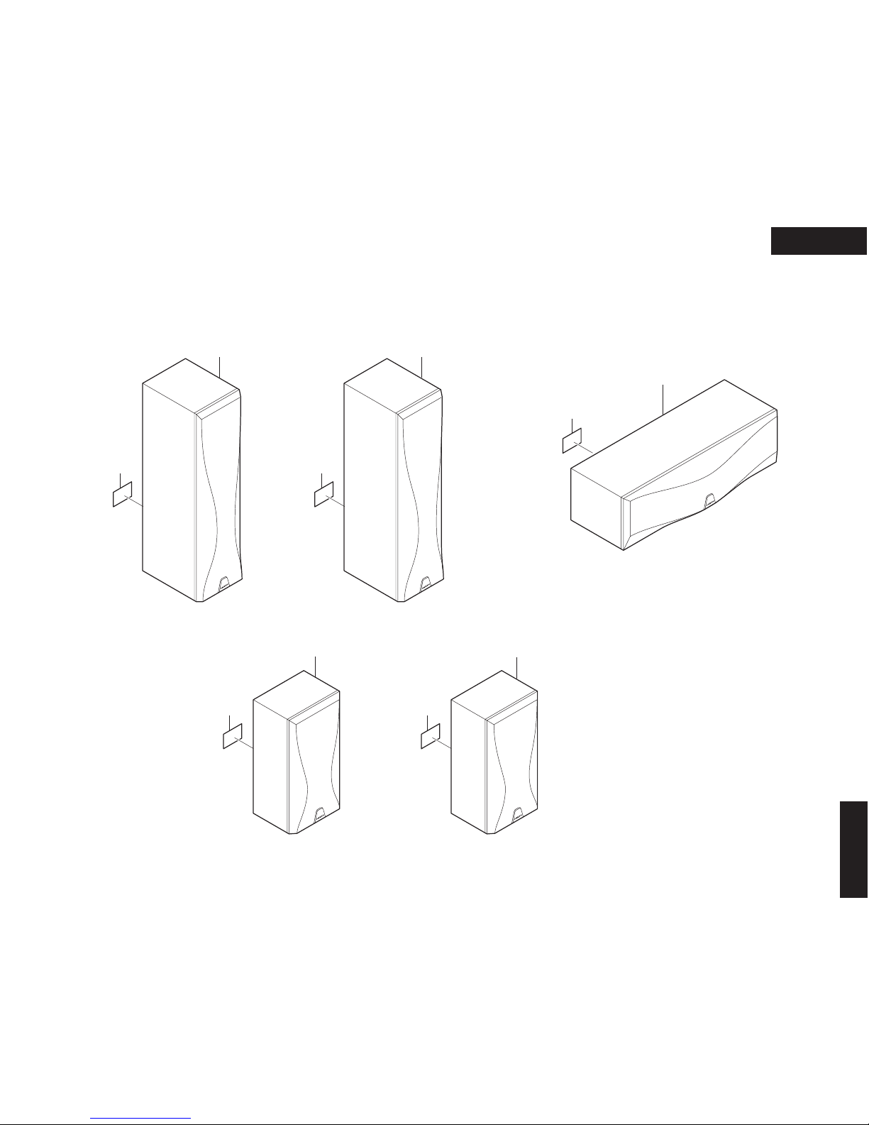
Front Speaker (SKF-420F)
Type :
Impedance :
Maximum input power :
Output sound pressure level :
Frequency response :
Crossover frequency :
Cabinet capacity :
Dimensions (W x H x D) :
Weight :
Drivers unit :
Terminal :
Other :
2-way Bass-reflex
8 ohm
100 W
84 dB/W/m
60 Hz - 50 kHz
5 kHz
0.2 cubic feet (5.6L)
4-7/8" x 18-5/16" x 7-1/16"
(124 x 465 x 179 mm)
7.5 lbs. (3.4 kg)
4 inch Cone Woofer x 2
1 inch Balanced Dome tweeter
Color-coded push type
Magnetic shielding
Type :
Impedance :
Maximum input power :
Output sound pressure level :
Frequency response :
Crossover frequency :
Cabinet capacity :
Dimensions (W x H x D) :
Weight :
Drivers unit :
Terminal :
Other :
2 Way Bass-reflex
8 ohm
100 W
84 dB/W/m
60 Hz - 50 kHz
5 kHz
0.2 cubic feet (5.6 L)
17-1/8" x 5-1/8" x 7-1/16"
(435 x 130 x 179 mm)
7.5 lbs. (3.4 kg)
4 inch Cone Woofer x 2
1 inch Balanced Dome tweeter
Color-coded push type
Magnetic shielding
Surround Speaker (SKM-420S)
Type :
Impedance :
Maximum input power :
Output sound pressure level :
Frequency response :
Crossover frequency :
Cabinet capacity :
Dimensions (W x H x D) :
Weight :
Drivers unit :
Terminal :
2-way Bass-reflex
8 ohm
100 W
82 dB/W/m
60 Hz - 50 kHz
5 kHz
0.08 cubic feet (2.3 L)
5-13/16" x 11" x 4-7/8"
(147 x 280 x 124 mm)
3.7 lbs. (1.7 kg)
4 inch Cone Woofer
1 inch Balanced Dome tweeter
Color-coded push type
Specifications and appearance are subject to change
without prior notice.
Powered Subwoofer (SKW-420) Center Speaker (SKC-420C)

HTP-420
EXPLODED VIEWS-1
SKW-420 : POWERED SUBWOOFER
HTP-420
A02
SP06
x 10 pcs.
A05 x 4 pcs.
A04
F903
A03
U02
U03
F902
A01
U01
A06
<Note>
IC501---> Refer to "PRINTED CIRCUIT BOARD PARTS LIST"
Refer to "EXPLODED VIEWS-2"
MDD type
MDC type
MDT type
MPA type
MGT type
MPT type
<Notes>
A06 (POWER SWITCH) :
MDD type
MDC type
MDT type
MPA type
MGT type
MPT type
--- No
--- No
--- No
--- Yes
--- Yes
--- Yes

HTP-420
EXPLODED VIEWS-2
SKW-420 : POWERED SUBWOOFER
HTP-420
SP06
x 8 pcs.
SP08
SP04
SP01
SP03
SP05
x 8 pcs.
SP02
x 4 pcs.

HTP-420
EXPLODED VIEWS-3
SKF-420F / SKC-420C / SKM-420S
HTP-420
SP11 SP13
SP10 SP12
SP17 SP19
SP16 SP18
SP14
SP15
"SKF-420F (L)" "SKF-420F (R)"
"SKC-420C"
"SKM-420S (R)""SKM-420S (L)"
TERMINAL :
White / Black
TERMINAL :
Red / Black
TERMINAL :
Green / Black
TERMINAL :
Blue / Black
TERMINAL :
Gray / Black

HTP-420
BLOCK DIAGRAM
SKW-420 : POWERED SUBWOOFER
HTP-420

HTP-420
SCHEMATIC DIAGRAM
SKW-420 : POWERED SUBWOOFER
HTP-420
A
1
2
3
4
5
BCDEFGH
LINE
INPUT
OUTPUT
LEVEL
AC 120V / 60Hz
AC 220-230V / 50Hz
AC 230-240V / 50Hz
SPEAKER
INPUT PC BOARD
U02 MAIN PC BOARD
U01
VR / LED PC BOARD
U03
LED
RED : STANDBY
GREEN : ON
<Note>
POWER SWITCH* / C1**
MDD type
MDC type
MDT type
MPA type
MGT type
MPT type
--- No
--- No
--- No
--- Yes
--- Yes
--- Yes
*
**
***
***
<Note>
C913*** / C914***
MDD type
MDC type
MDT type
MPA type
MGT type
MPT type
--- Yes
--- Yes
--- Yes
--- No
--- No
--- No

HTP-420
SCHEMATIC DIAGRAM
SKW-420 : POWERED SUBWOOFER
A
1
2
3
4
5
BCDEFGH
LINE
INPUT
OUTPUT
LEVEL
AC 120V / 60Hz
AC 220-230V / 50Hz
AC 230-240V / 50Hz
SPEAKER
INPUT PC BOARD
U02 MAIN PC BOARD
U01
VR / LED PC BOARD
U03
LED
RED : STANDBY
GREEN : ON
<Note>
POWER SWITCH* / C1**
MDD type
MDC type
MDT type
MPA type
MGT type
MPT type
--- No
--- No
--- No
--- Yes
--- Yes
--- Yes
*
**
***
***
<Note>
C913*** / C914***
MDD type
MDC type
MDT type
MPA type
MGT type
MPT type
--- Yes
--- Yes
--- Yes
--- No
--- No
--- No

HTP-420
PC BOARD CONNECTION DIAGRAM
SKW-420 : POWERED SUBWOOFER
HTP-420
MAIN PC BOARD
VR / LED PC BOARD
INPUT PC BOARD
<Notes>
POWER SWITCH :
MDD type
MDC type
MDT type
MPA type
MGT type
MPT type
--- No
--- No
--- No
--- Yes
--- Yes
--- Yes
POWER SWITCH

HTP-420
PRINTED CIRCUIT BOARD VIEW
SKW-420 : POWERED SUBWOOFER
A
1
2
3
4
5
BCD
INPUT PC BOARD
U02
MAIN PC BOARD
U01
VR / LED PC BOARD
U03
No PC board view
Look over the actual PC board on hand

TDA7293
120V - 100W DMOS AUDIO AMPLIFIER WITH MUTE/ST-BY
VERY HIGH OPERATING VOLTAGE RANGE
(±50V)
DMOS POWER STAGE
HIGH OUTPUT POWER (100W @ THD =
10%, RL= 8Ω, VS= ±40V)
MUTING/STAND-BY FUNCTIONS
NO SWITCH ON/OFF NOISE
VERY LOW DISTORTION
VERY LOW NOISE
SHORT CIRCUIT PROTECTED (WITH NO IN-
PUT SIGNAL APPLIED)
THERMAL SHUTDOWN
CLIP DETECTOR
MODULARITY (MORE DEVICES CAN BE
EASILY CONNECTED IN PARALLEL TO
DRIVE VERY LOW IMPEDANCES)
DESCRIPTION
The TDA7293 is a monolithic integrated circuit in
Multiwatt15 package, intended for use as audio
class AB amplifier in Hi-Fi field applications
(Home Stereo, self powered loudspeakers, Top-
class TV). Thanks to the wide voltage range and
to the high out current capability it is able to sup-
ply the highest power into both 4Ωand 8Ωloads.
The built in muting function with turn on delay
simplifies the remote operation avoiding switching
on-off noises.
Parallel mode is made possible by connecting
more device through of pin11. High output power
can be delivered to very low impedance loads, so
optimizing the thermal dissipation of the system.
January 2003
®
IN- 2
R2
680Ω
C2
22µF
C1 470nF IN+
R1 22K
3
R3 22K
-
+
MUTE
STBY
4
VMUTE
VSTBY
10
9
SGND
MUTE
STBY
R4 22K
THERMAL
SHUTDOWN S/C
PROTECTION
R5 10K
C3 10µF C4 10µF
1
STBY-GND
C5
22µF
713
14
6
158
-Vs -PWVs
BOOTSTRAP
OUT
+PWVs+Vs
C9 100nF C8 1000µF
-Vs
D97AU805A
+Vs
C7 100nF C6 1000µF
BUFFER DRIVER
11
BOOT
LOADER
12
5VCLIP
CLIP DET
(*)
(*) see Application note
(**) for SLAVE function
(**)
Figure 1: Typical Application and Test Circuit
Multiwatt15V Multiwatt15H
ORDERING NUMBERS:
TDA7293V TDA7293HS
MULTIPOWER BCD TECHNOLOGY
1/15

ABSOLUTE MAXIMUM RATINGS
Symbol Parameter Value Unit
VSSupply Voltage (No Signal) ±60 V
V1VSTAND-BY GND Voltage Referred to -VS(pin 8) 90 V
V2Input Voltage (inverting) Referred to -VS90 V
V2- V3Maximum Differential Inputs ±30 V
V3Input Voltage (non inverting) Referred to -VS90 V
V4Signal GND Voltage Referred to -VS90 V
V5Clip Detector Voltage Referred to -VS120 V
V6Bootstrap Voltage Referred to -VS120 V
V9Stand-by Voltage Referred to -VS120 V
V10 Mute Voltage Referred to -VS120 V
V11 Buffer Voltage Referred to -VS120 V
V12 Bootstrap Loader Voltage Referred to -VS100 V
IOOutput Peak Current 10 A
Ptot Power Dissipation Tcase = 70°C50W
T
op Operating Ambient Temperature Range 0 to 70 °C
Tstg, TjStorage and Junction Temperature 150 °C
1
2
3
4
5
6
7
9
10
11
8
BUFFER DRIVER
MUTE
STAND-BY
-V
S
(SIGNAL)
+V
S
(SIGNAL)
BOOTSTRAP
CLIP AND SHORT CIRCUIT DETECTOR
SIGNAL GROUND
NON INVERTING INPUT
INVERTING INPUT
STAND-BY GND
TAB CONNECTED TO PIN 8
13
14
15
12
-V
S
(POWER)
OUT
+V
S
(POWER)
BOOTSTRAP LOADER
D97AU806
PIN CONNECTION (Top view)
THERMAL DATA
Symbol Description Typ Max Unit
Rth j-case Thermal Resistance Junction-case 1 1.5 °C/W
TDA7293
2/15

ELECTRICAL CHARACTERISTICS (Refer to the Test Circuit VS= ±40V, RL= 8Ω, Rg= 50 Ω;
Tamb = 25°C, f = 1 kHz; unless otherwise specified).
Symbol Parameter Test Condition Min. Typ. Max. Unit
VSSupply Range ±12 ±50 V
IqQuiescent Current 50 100 mA
IbInput Bias Current 0.3 1 µA
VOS Input Offset Voltage -10 10 mV
IOS Input Offset Current 0.2 µA
PORMS Continuous Output Power d = 1%:
RL= 4Ω; VS= ±29V, 75 80
80 W
d = 10%
RL= 4Ω ; VS= ±29V 90 100
100 W
d Total Harmonic Distortion (**) PO= 5W; f = 1kHz
PO= 0.1 to 50W; f = 20Hz to 15kHz 0.005 0.1 %
%
ISC Current Limiter Threshold VS≤±40V 6.5 A
SR Slew Rate 5 10 V/µs
GVOpen Loop Voltage Gain 80 dB
GVClosed Loop Voltage Gain (1) 29 30 31 dB
eNTotal Input Noise A = curve
f = 20Hz to 20kHz 1
310
µ
V
µ
V
R
iInput Resistance 100 kΩ
SVR Supply Voltage Rejection f = 100Hz; Vripple = 0.5Vrms 75 dB
TSThermal Protection DEVICE MUTED 150 °C
DEVICE SHUT DOWN 160 °C
STAND-BY FUNCTION (Ref: to pin 1)
VST on Stand-by on Threshold 1.5 V
VST off Stand-by off Threshold 3.5 V
ATTst-by Stand-by Attenuation 70 90 dB
Iq st-by Quiescent Current @ Stand-by 0.5 1 mA
MUTE FUNCTION (Ref: to pin 1)
VMon Mute on Threshold 1.5 V
VMoff Mute off Threshold 3.5 V
ATTmute Mute AttenuatIon 60 80 dB
CLIP DETECTOR
Duty Duty Cycle ( pin 5) THD = 1% ; RL = 10KΩ to 5V 10 %
THD = 10% ;
RL = 10KΩto 5V 30 40 50 %
ICLEAK PO = 50W 3 µA
SLAVE FUNCTION pin 4 (Ref: to pin 8 -VS)
VSlave SlaveThreshold 1V
V
Master Master Threshold 3 V
Note (1): GVmin ≥ 26dB
Note: Pin 11 only for modular connection. Max external load 1MΩ/10 pF, only for test purpose
Note (**): Tested with optimized Application Board (see fig. 2)
TDA7293
3/15

Figure 2: Typical Application P.C. Board and Component Layout (scale 1:1)
TDA7293
4/15

APPLICATION SUGGESTIONS (see Test and Application Circuits of the Fig. 1)
The recommended values of the external components are those shown on the application circuit of Fig-
ure 1. Different values can be used; the following table can help the designer.
COMPONENTS SUGGESTED VALUE PURPOSE LARGER THAN
SUGGESTED SMALLER THAN
SUGGESTED
R1 (*) 22k INPUT RESISTANCE INCREASE INPUT
IMPEDANCE DECREASE INPUT
IMPEDANCE
R2 680ΩCLOSED LOOP GAIN
SET TO 30dB (**) DECREASE OF GAIN INCREASE OF GAIN
R3 (*) 22k INCREASE OF GAIN DECREASE OF GAIN
R4 22k ST-BY TIME
CONSTANT LARGER ST-BY
ON/OFF TIME SMALLER ST-BY
ON/OFF TIME;
POP NOISE
R5 10k MUTE TIME
CONSTANT LARGER MUTE
ON/OFF TIME SMALLER MUTE
ON/OFF TIME
C1 0.47µF INPUT DC
DECOUPLING HIGHER LOW
FREQUENCY
CUTOFF
C2 22µF FEEDBACK DC
DECOUPLING HIGHER LOW
FREQUENCY
CUTOFF
C3 10µF MUTE TIME
CONSTANT LARGER MUTE
ON/OFF TIME SMALLER MUTE
ON/OFF TIME
C4 10µF ST-BY TIME
CONSTANT LARGER ST-BY
ON/OFF TIME SMALLER ST-BY
ON/OFF TIME;
POP NOISE
C5 22µFXN (***) BOOTSTRAPPING SIGNAL
DEGRADATION AT
LOW FREQUENCY
C6, C8 1000µF SUPPLY VOLTAGE
BYPASS
C7, C9 0.1µF SUPPLY VOLTAGE
BYPASS DANGER OF
OSCILLATION
(*) R1 = R3 for pop optimization
(**) Closed Loop Gain has to be ≥26dB
(***) Multiplay this value for the number of modular part connected
MASTER
UNDEFINED
SLAVE
-V
S
+3V
-V
S
+1V
-V
S
D98AU821
Slave function: pin 4 (Ref to pin 8 -VS)Note:
If in the application, the speakers are connected
via long wires, it is a good rule to add between
the output and GND, a Boucherot Cell, in order to
avoid dangerous spurious oscillations when the
speakers terminal are shorted.
The suggested Boucherot Resistor is 3.9Ω/2W
and the capacitor is 1µF.
TDA7293
5/15

INTRODUCTION
In consumer electronics, an increasing demand
has arisen for very high power monolithic audio
amplifiers able to match, with a low cost, the per-
formance obtained from the best discrete de-
signs.
The task of realizing this linear integrated circuit
in conventional bipolar technology is made ex-
tremely difficult by the occurence of 2nd break-
down phoenomenon. It limits the safe operating
area (SOA) of the power devices, and, as a con-
sequence, the maximum attainable output power,
especially in presence of highly reactive loads.
Moreover, full exploitation of the SOA translates
into a substantial increase in circuit and layout
complexity due to the need of sophisticated pro-
tection circuits.
To overcome these substantial drawbacks, the
use of power MOS devices, which are immune
from secondary breakdown is highly desirable.
The device described has therefore been devel-
oped in a mixed bipolar-MOS high voltage tech-
nology called BCDII 100/120.
1) Output Stage
The main design task in developping a power op-
erational amplifier, independently of the technol-
ogy used, is that of realization of the output stage.
The solution shown as a principle shematic by
Fig3 represents the DMOS unity - gain output
buffer of the TDA7293.
This large-signal, high-power buffer must be ca-
pable of handling extremely high current and volt-
age levels while maintaining acceptably low har-
monic distortion and good behaviour over
frequency response; moreover, an accurate con-
trol of quiescent current is required.
A local linearizing feedback, provided by differen-
tial amplifier A, is used to fullfil the above require-
ments, allowing a simple and effective quiescent
current setting.
Proper biasing of the power output transistors
alone is however not enough to guarantee the ab-
sence of crossover distortion.
While a linearization of the DC transfer charac-
teristic of the stage is obtained, the dynamic be-
haviour of the system must be taken into account.
A significant aid in keeping the distortion contrib-
uted by the final stage as low as possible is pro-
vided by the compensation scheme, which ex-
ploits the direct connection of the Miller capacitor
at the amplifier’s output to introduce a local AC
feedback path enclosing the output stage itself.
2) Protections
In designing a power IC, particular attention must
be reserved to the circuits devoted to protection
of the device from short circuit or overload condi-
tions.
Due to the absence of the 2nd breakdown phe-
nomenon, the SOA of the power DMOS transis-
tors is delimited only by a maximum dissipation
curve dependent on the duration of the applied
stimulus.
In order to fully exploit the capabilities of the
power transistors, the protection scheme imple-
mented in this device combines a conventional
SOA protection circuit with a novel local tempera-
ture sensing technique which " dynamically" con-
trols the maximum dissipation.
Figure 3: Principle Schematic of a DMOS unity-gain buffer.
TDA7293
6/15

In addition to the overload protection described
above, the device features a thermal shutdown
circuit which initially puts the device into a muting
state (@ Tj = 150 oC) and then into stand-by (@
Tj = 160 oC).
Full protection against electrostatic discharges on
every pin is included.
3) Other Features
The device is provided with both stand-by and
mute functions, independently driven by two
CMOS logic compatible input pins.
The circuits dedicated to the switching on and off
of the amplifier have been carefully optimized to
avoid any kind of uncontrolled audible transient at
the output.
The sequence that we recommend during the
ON/OFF transients is shown by Figure 4.
The application of figure 5 shows the possibility of
using only one command for both st-by and mute
functions. On both the pins, the maximum appli-
cable range corresponds to the operating supply
voltage.
APPLICATION INFORMATION
HIGH-EFFICIENCY
Constraints of implementing high power solutions
are the power dissipation and the size of the
power supply. These are both due to the low effi-
ciency of conventional AB class amplifier ap-
proaches.
Here below (figure 6) is described a circuit pro-
posal for a high efficiency amplifier which can be
adopted for both HI-FI and CAR-RADIO applica-
tions.
1N4148
10K 30K
20K
10µF10µF
MUTE STBY
D93AU014
MUTE/
ST-BY
Figure 5: Single Signal ST-BY/MUTE Control
Circuit
PLAY
OFF
ST-BY
MUTE MUTE
ST-BY OFF
D98AU817
5V
5V
+Vs
(V)
+40
-40
VMUTE
PIN #10
(V)
VST-BY
PIN #9
(V)
-Vs
VIN
(mV)
IQ
(mA)
VOUT
(V)
Figure 4: Turn ON/OFF Suggested Sequence
TDA7293
7/15

The TDA7293 is a monolithic MOS power ampli-
fier which can be operated at 100V supply voltage
(120V with no signal applied) while delivering out-
put currents up to ±6.5 A.
This allows the use of this device as a very high
power amplifier (up to 180W as peak power with
T.H.D.=10 % and Rl = 4 Ohm); the only drawback
is the power dissipation, hardly manageable in
the above power range.
The typical junction-to-case thermal resistance of
the TDA7293 is 1 oC/W (max= 1.5 oC/W). To
avoid that, in worst case conditions, the chip tem-
perature exceedes 150 oC, the thermal resistance
of the heatsink must be 0.038 oC/W (@ max am-
bient temperature of 50 oC).
As the above value is pratically unreachable; a
high efficiency system is needed in those cases
where the continuous RMS output power is higher
than 50-60 W.
The TDA7293 was designed to work also in
higher efficiency way.
For this reason there are four power supply pins:
two intended for the signal part and two for the
power part.
T1 and T2 are two power transistors that only
operate when the output power reaches a certain
threshold (e.g. 20 W). If the output power in-
creases, these transistors are switched on during
the portion of the signal where more output volt-
age swing is needed, thus "bootstrapping" the
power supply pins (#13 and #15).
The current generators formed by T4, T7, zener
diodes Z1, Z2 and resistors R7,R8 define the
minimum drop across the power MOS transistors
of the TDA7293. L1, L2, L3 and the snubbers C9,
R1 and C10, R2 stabilize the loops formed by the
"bootstrap" circuits and the output stage of the
TDA7293.
By considering again a maximum average
output power (music signal) of 20W, in case
of the high efficiency application, the thermal
resistance value needed from the heatsink is
2.2oC/W (Vs =±50 V and Rl= 8 Ohm).
All components (TDA7293 and power transis-
tors T1 and T2) can be placed on a 1.5oC/W
heatsink, with the power darlingtons electrically
insulated from the heatsink.
Since the total power dissipation is less than that
of a usual class AB amplifier, additional cost sav-
ings can be obtained while optimizing the power
supply, even with a high heatsink .
BRIDGE APPLICATION
Another application suggestion is the BRIDGE
configuration, where two TDA7293 are used.
In this application, the value of the load must not
be lower than 8 Ohm for dissipation and current
capability reasons.
A suitable field of application includes HI-FI/TV
subwoofers realizations.
The main advantages offered by this solution are:
- High power performances with limited supply
voltage level.
- Considerably high output power even with high
load values (i.e. 16 Ohm).
With Rl= 8 Ohm, Vs = ±25V the maximum output
power obtainable is 150 W, while with Rl=16
Ohm, Vs = ±40V the maximum Pout is 200 W.
APPLICATION NOTE: (ref. fig. 7)
Modular Application (more Devices in Parallel)
The use of the modular application lets very high
power be delivered to very low impedance loads.
The modular application implies one device to act
as a master and the others as slaves.
The slave power stages are driven by the master
device and work in parallel all together, while the in-
put and the gain stages of the slave device are dis-
abled, the figure below shows the connections re-
quired to configure two devices to work together.
The master chip connections are the same as
the normal single ones.
The outputs can be connected together with-
out the need of any ballast resistance.
The slave SGND pin must be tied to the nega-
tive supply.
The slave ST-BY and MUTE pins must be con-
nected to the master ST-BY and MUTE pins.
The bootstrap lines must be connected to-
gether and the bootstrap capacitor must be in-
creased: for N devices the boostrap capacitor
must be 22µF times N.
The slave IN-pin must be connected to the
negative supply.
THE BOOTSTRAP CAPACITOR
For compatibility purpose with the previous de-
vices of the family, the boostrap capacitor can be
connected both between the bootstrap pin (6) and
the output pin (14) or between the boostrap pin
(6) and the bootstrap loader pin (12).
When the bootcap is connected between pin 6
and 14, the maximum supply voltage in presence
of output signal is limited to 100V, due the boot-
strap capacitor overvoltage.
When the bootcap is connected between pins 6
and 12 the maximum supply voltage extend to the
full voltage that the technology can stand: 120V.
This is accomplished by the clamp introduced at
the bootstrap loader pin (12): this pin follows the
output voltage up to 100V and remains clamped
at 100V for higher output voltages. This feature
lets the output voltage swing up to a gate-source
voltage from the positive supply (VS-3 to 6V).
TDA7293
8/15

TDA7293
3
1
4
137
815
2
14
6
10
R3 680 C11 22µF
L3 5µH
R18 270
R16
13K
C15
22µF
9
R12
13K
C13 10µF
R13 20K
C12 330nF
R15 10K
C14
10µF
R14 30K
D5
1N4148
PLAY
ST-BY
R17 270
L1 1µH
T1
BDX53A
T3
BC394
D3 1N4148
R4
270 R5
270
T4
BC393 T5
BC393
R6
20K
R7
3.3K C16
1.8nF
R8
3.3K C17
1.8nF
Z2 3.9V
Z1 3.9V
L2 1µH
R19 270
D4 1N4148
D2 BYW98100
R1
2
R2
2
C9
330nF
C10
330nF
T2
BDX54A T6
BC393
T7
BC394 T8
BC394
R9
270 R10
270 R11
20K
OUT
INC7
100nF
C5
1000µF
35V
C8
100nF
C6
1000µF
35V
C1
1000µF
63V
C2
1000µF
63V
C3
100nF
C4
100nF
+50V
+25V D1 BYW98100
GND
-25V
-50V
D97AU807C
12
D6
1N4001
R20
20K
R21
20K
D7
1N4001
R22
10K
R23
10K
P
ot
Figure 6: High Efficiency Application Circuit
Figure 6a: PCB and Component Layout of the fig. 6
TDA7293
9/15
This manual suits for next models
2
Table of contents
Other Onkyo Home Cinema Speakers manuals

Onkyo
Onkyo HTP-960 User manual

Onkyo
Onkyo HT-R667 User manual

Onkyo
Onkyo HTP-540 User manual

Onkyo
Onkyo SKS-HT870 - 7.1-CH Home Theater Speaker Sys User manual

Onkyo
Onkyo HT-R560 User manual

Onkyo
Onkyo HTP-678 User manual

Onkyo
Onkyo SKW-940 User manual

Onkyo
Onkyo SKS-HT528B User manual

Onkyo
Onkyo HTP-528 User manual

Onkyo
Onkyo HTP-518 User manual

Onkyo
Onkyo HTP-940 User manual

Onkyo
Onkyo HTP-338 User manual

Onkyo
Onkyo HTP-750B User manual

Onkyo
Onkyo HTP-750 User manual

Onkyo
Onkyo HTP-993 User manual

Onkyo
Onkyo HTP-240(S) User manual

Onkyo
Onkyo SKS-HT320 User manual

Onkyo
Onkyo SKS-HT540(B) User manual

Onkyo
Onkyo HTP-555 User manual

Onkyo
Onkyo SKW-580 User manual