NCV78343EVBUM
www.onsemi.com
3
GETTING STARTED
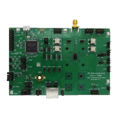
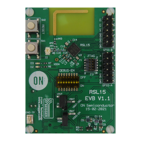
The evaluation board is supplied through either banana
or standard 5.5 x 2.5 mm DC connectors. Supply voltage
range has to be from 8 to 40 V. LEDs can be optionally
powered from boost−buck converter board
NCV78763R1DAGEVB in the slot position J.BCKx.y.
The default system architecture uses repeater−slave device
at U1 position and slave device at U2 position. Local
M−LVDS bus which requires two 100 Wterminating
resistors is also used in this configuration. To ensure proper
termination please short both J_LVDS1 and J_LVDS2
connectors.
Plug−in the USB cable to the ONMCU board and start
the PC SW GUI application. The COM port should be
loaded automatically, otherwise please click on Refresh
button and then on Connect. If the COM port is not
available, please check installed drivers (see below).
SYSTEM ARCHITECTURE
The evaluation kit supports different system architectures.
The main differences are how the devices communicate with
the MCU.
1. UART →CAN (default configuration)
ONMCU UART →CAN →1st NCV78343
→M−LVDS →2nd NCV78343 →M−LVDS
2. MCU UART through M−LVDS
ONMCU UART →1st NCV78343 →
M−LVDS →2nd NCV78343 →M−LVDS
3. Only M−LVDS
ONMCU UART →M−LVDS →
1st NCV78343 →M−LVDS →
2nd NCV78343 →M−LVDS
4. Only MCU UART
ONMCU UART →1st NCV78343
and 2nd NCV78343 (common UART)
5. CAN UART through M−LVDS
External CAN →1st NCV78343 →M−LVDS
→2nd NCV78343 →M−LVDS
6. Only CAN UART
External CAN →1st NCV78343
and 2nd NCV78343 (common UART)
It is possible to change the system architecture just by
replacing 0 Wresistors following the configuration sheet
in the schematic document. The default configuration
uses UART communication over CAN physical layer.
The CAN loop is made by two NCV7344 CAN
transceivers. This simulates real application, where
the CAN physical layer is used in the headlamp. In this
configuration the first NCV78343 device U1 must be
configured as a repeater−slave and the second device U2 has
to be configured as a slave and also both J_LVDS pin
headers must be shorted.
ADC Inputs
Each NCV78343 has three ADC inputs which share
two functions. ADC0 and ADC1 share the functionality
with I2C and ADC2 shares the functionality with input
address resistor divider. All three ADC inputs are available
at J_ADC_xA connectors. The first U1 device has by default
external I2C EEPROM memory connected to pins SDA
and SCL, while the second U2 device has all three
ADC inputs connected to the resistor divider.
Addressing
NCV78343 devices are by default supplied without
content in customer OTP memory bank (not zapped).
This allows full configuration flexibility. When using not
zapped devices, it is possible to address them by resistor
divider connected to ADC2/ADR pin or by the
auto−addressing process (described below). Default
addresses determined by voltage divider on ADC2/ADR pin
are ‘4’ for U1 and ‘7’ for U2.
Zapped devices have their address determined by
the contents of OTP memory bank.
First LED control
Run the SW GUI and click on Connect button in
the bottom menu. If the COM port is not recognized, click
on Refresh button or check installed drivers (see below).
An application window will automatically pop up. Devices
should be addressed using address from OTP memory,
resistor divider or auto−addressing.
The read OPMODE command should return “direct”
OPMODE for both devices with zapped OTP memory.
Enable “Autoupdate” checkbox and both BUCKx EN if the
NCV78763 BOOST−BUCK module is available. Now, it is
possible to independently move with each slider, and
according to this the LED brightness should be changing.
