EVBUM2817/D
www.onsemi.com
2
Key Features (continued)
•User Programmable Dead−Time
•Available Package Footprint
♦Type−A : TO−220, TO−3P, TO−247, D−PAK, and D2PAK
♦Type−B : TO−247−4L
♦Type−C : D2PAK−7L
EVALUATION BOARD OPERATION
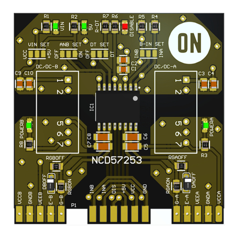
This section describes how to operate the NCP51561
evaluation board (EVB). Make external connections to the
NCP51561 EVB using either the installed test−points or by
installing wires into the connectors. The main connections
that must be made to the EVB are the analog supply voltage,
input signal, and output load and monitoring equipment.
Features
•Evaluation board for the NCP51561 product family in a
wide body SOIC−16 package.
•3−V to 5.0−V VDD power supply range, and up to 30−V
VCCA/VCCB power supply range.
•4.5−A and 9−A source/sink current driving capability.
•TTL −compatible inputs
•Allowable input voltage up to 18−V with for INA, INB,
and ANB pins.
•Onboard trimmer potentiometer for dead−time
programming.
•3−position header with for INA, INB, and ENA/DIS
pins.
•2−position header with for ANB pin.
•Support for half−bridge test with MOSFETs, and SiC
MOSFETs with connection to external power stage.
Power and Ground
NOTE: Connecting the all power supplies in reverse
polarity (backwards) will instantly device when
power is turned on and device damage can result.
The primary side of the EVM (VDD) operates from a
single 3−V to 5.0−V power supply and connected via J2. Test
point (TP6 and TP7) is available for monitoring the primary
power supply.
The EVM provides connections for evaluating the output
side (VCCA, VSSA, VCCB, and VSSB) power supplies for the
channel A and B, from a minimum 6.5−V to maximum 30−V
for 5−V UVLO version as shown in Figure 4 and Figure 5.
VCCA and VCCB can be monitored via TP3 and TP11,
respectively.
The VCCA and VCCB pin should be bypassed with a
capacitor with a value of at least ten times the gate
capacitance, and over 100 nF and located as close to the
device as possible for the purpose of decoupling. A low
ESR, ceramic surface mount capacitor is necessary. We had
recommends using 2 capacitors; a over 100 nF ceramic
surface−mount capacitor, and another a tantalium or
electrolytic capacitor of few microfarads added in parallel.
Input and Output
1. Connection of primary−side power supply to the
VDD connector [J2].
2. Connection of secondary−side power supply to the
VCCA and VCCB connector [J9, and J13].
3. Connection of INA signal to the SIGNAL
connector [J1−1, and J4].
4. Connection of INB signal to the SIGNAL
connector [J1−2, and J5].
5. Connection of ENABLE or DISABLE signal to
the ENA/DIS connector [J1−3, and J15].
6. Connection of ANB signal to the ANB jumper
[J11].
Notes for NCP51560/563 Use on these Boards
NCP51560:
•Unsolder NCP51561 unit and solder back NCP51560
option you want to test.
•Please don’t use any features related to ANB pin − see
jumper sections.
NCP/V51563:
•Just unsolder NCP51561 unit and solder back
NCP51563/NCV51563 option you want to test.
•All the rest stays unchanged.
