EVBUM2757/D
www.onsemi.com
4
Before measuring power consumption, load the Sleep
Mode sample application onto the RSL15 Evaluation and
Development Board with the desired settings:
1. Disable the usage of GPIOs for lowest consumption.
2. Configure either the 32 kHz crystal (XTAL32) or the
32 kHz RC oscillator (RCOSC32) as the source for
STANDBYCLK.
3. Configure the DCDC regulator for either buck mode
or LDO mode.
4. Configure the RTC clock wakeup duration. This
determines the time between device wakeup states.
When measuring power consumption, ensure a large
enough time difference between wakeup pulses.
There is a capacitor on VCC which is a part of the
DC/DC regulator that powers the device and the
wakeup period should allow for this capacitor to
fully discharge, thus resulting in accurate values.
A longer wakeup period is recommended since the
measurement values in the datasheet were taken
after the VCC capacitor had discharged. Power
consumption values will be an average value taken
over 4 seconds. Therefore a wakeup period of at least
8 seconds is ideal.
5. In order to change the amount of RAM that is kept
in retention, the #defines in the code as well as the
linker script will need to be modified.
Take the power consumption measurements:
6. Follow the hardware setup steps in section Power
Measurement Setup.
7. Turn on the measurement instrument.
8. Set the output voltage. This will depend on the mode
the DCDC is in. If in LDO mode, the output voltage
should be 1.25 V or 1.5 V. If in buck mode, the output
voltage should be 1.8 V or 3 V.
9. Set the output current range to the lowest setting that
permits accurate measurements. Note that selection
of an appropriate measurement range when
measuring low currents, especially in the nA range,
is extremely important for generating accurate
results.
10. Enable the power supply such that power
consumption measurements can be taken.
11. On the RSL15 Evaluation and Development Board,
press the RESET button to restart the sample
application on the board. As a best practice, this
should be done in between all measurements.
12. Measure the power consumption over a period of
4 seconds, preferably right before a wakeup pulse to
ensure that the VCC capacitor has discharged
completely. Take a minimum of 3 measurements and
average these values to obtain the most accurate
results.
Communication
There are two ways of achieving communication with the
RSL15 Evaluation and Development Board.
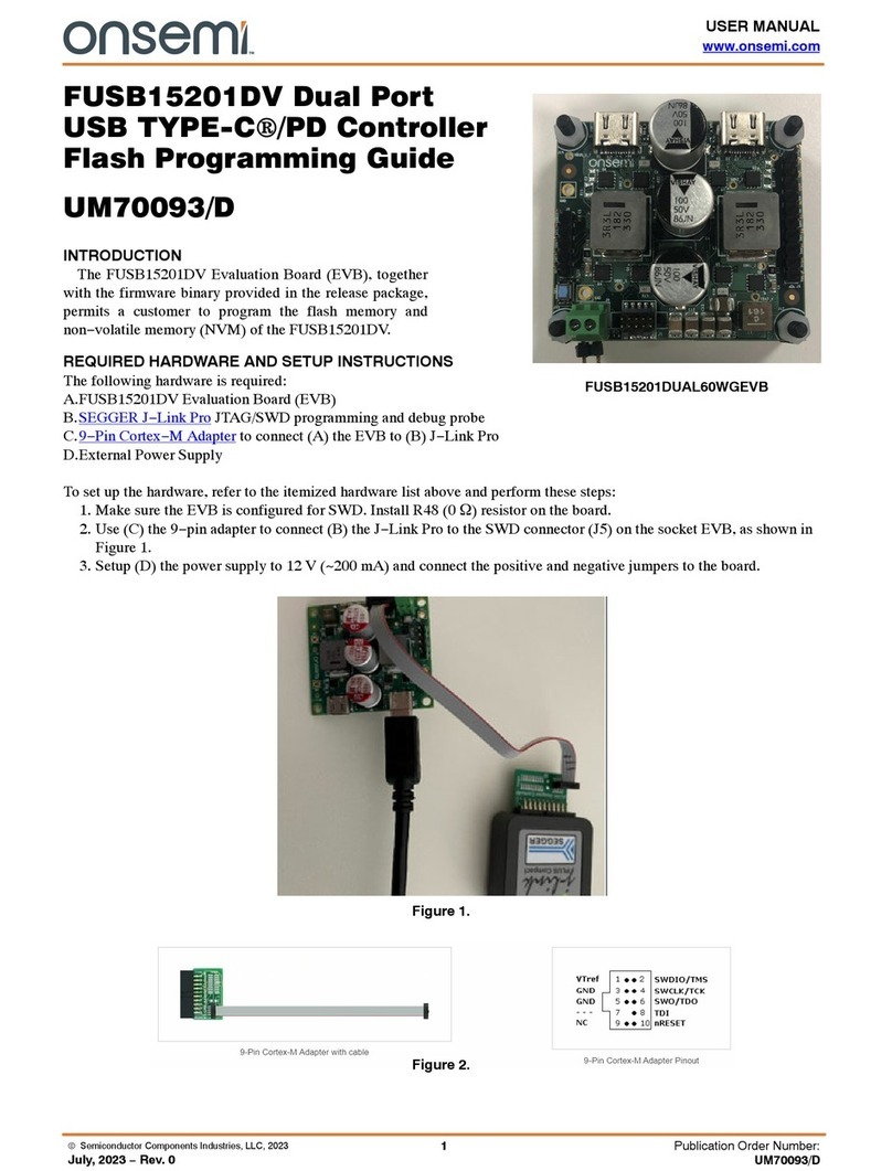
The USB−C 2.0 connection (J6) is connected to a J−Link
onboard solution that provides an SWJ−DP for debugging
the RSL15 at up to 4 MHz. The TC2050−IDC connector (J8
header) is used to program the Arm®Cortex®−M4
processor with J−Link firmware. The EVB is configured for
this use case by default. See Figure 2. Standard USB
connection.
In order for the USB connection to work, the shorting
jumpers must be in their default position. The first jumper
must be placed across VBAT and VOUT on the VBAT-SEL
header. The second jumper must be placed on VDDO−EN,
shorting VDDO and VBAT.
It is also possible to connect and debug the RSL15 via the
10−pin JTAG (JTAG header) connector. This connector is
compatible with J−Link debugging devices when paired
with an adapter: https://www.olimex.com/Products/
ARM/JTAG/ARM−JTAG−20−10/. See Figure 3.
The simplest method for configuring the device to be
programmed or debugged is by using the standard USB
connection.
UART over J−Link On−board
When the RSL15 EVB is connected to a host Windows PC
via the USB−C cable, a UART is available between the PC
and the RSL15 via the J−Link On−board. If J−Link drivers
are installed, the device shows up in Windows Device
Manager under Ports as a JLink CDC UART Port. Standard
software or libraries that are commonly used for serial
monitor purposes work with this serial port. GPIO5 is
connected to the TXD line of the J−Link OB UART, and
GPIO6 is connected to RXD. Therefore, in firmware on the
RSL15, GPIO6 and GPIO5 need to be configured in the
same manner, where the RSL15 GPIO6 is configured as the
UART TXD pin and GPIO5 is configured as the RXD pin.
The UART supports up to 115200 baud.
The UART can be enabled or disabled mechanically on
the EVB, using the DIP switch labelled DEBUG−EN. If
position 7 and 8 on the DIP switch are placed in the OFF
position, then the UART is disabled. Placing both position 7
and 8 back to the ON position re−enables the UART.
Position 3 of the DIP switch must be in the ON position as
well, as this enables the level shifters between the J−Link OB
and the RSL15.
Figure 2. Standard USB Connection
USB−C Cable
Host PC
RSL15
Evaluation and
Development
Board
