ORTEC 467 Service manual

Model
467
Time
to
Pulse
Height
Converter
and
SCA
Operating
and
Service
Manual
This
manual
applies
to
instruments
marked
"Rev
12"
(on
rear
panel)
7V.
Printed
in
U.S.A.
2730
(N152Q)
02C
0976

CONTENTS
Page
WARRANTY
v
PHOTOGRAPHS
vi
1.
DESCRIPTION
1
1.1.
Purpose
and
Features
1
1.2.
Operation
1
1.3.
Logic
1
2.
SPECIFICATIONS
2
2.1.
Performance
2
2.2.
Controls
3
2.3.
Inputs
3
2.4.
Outputs
3
2.5.
Electrical
and
Mechanical
4
3.
INSTALLATION
4
3.1.
General
4
3.2.
Connection
to
Power
4
3.3.
Connection
into
a
System
4
3.4.
Linear
Output
Signal
Connections
and
Terminating
Impedance
5
3.5.
Logic
Signal
Connections
5
4.
OPERATING
INSTRUCTIONS
5
4.1.
Time
to
Pulse
Height
Conversion
5
4.2.
Single
Channel
Analysis
6
5.
CIRCUIT
DESCRIPTION
7
5.1.
General
7
5.2.
TPHC
Circuit
7
5.3.
Single
Channel
Analyzer
Circuit
8
5.4.
Auxiliary
Logic
8
6.
MAINTENANCE
9
6.1.
Testing
Performance
9
6.2.
Corrective
Maintenance
12
6.3.
Troubleshooting
14
6.4.
Typical
DC
Voltages
15
6.5.
Modifications
15
6.6.
Factory
Repair
15
Schematics
and
Block
Diagram
467-0201-S1
467-0301-S1
467-0101-B1

ILLUSTRATIONS
Fig.
6.1.
Test
System
for
Checking
Conversion
9
Fig.
6.2.
Test
System
for
Checking
Converter
Resolution
10
Fig.
6.3.
Test
System
for
Checking
Count
Rate
11
Fig.
6.4.
Test
System
for
Checking
Differential
Linearity
11
Fig.
6.5.
Differential
Linearity
for
the
Indicated
Ranges
11
Fig.
6.6.
Test
System
for
Checking
External
Strobing
Mode
12
Fig.
6.7.
Using
Internal
Strobe
with
Stop
After
End
of
Conversion
13
Fig.
6.8.
Using
Internal
Strobe
with
Stop
Timed
Normally
13
Fig.
6.9.
Using
External
Strobe
with
Output
Timed
Normally
14
Fig.
6.10.
Using
External
Strobe
with
Strobe
Signal
Arriving
Before
Conversion
is
Complete
14
STANDARD
WARRANTY
FOR
ORTEC
INSTRUMENTS
ORTEC
warrants
that
the
items
will
be
delivered
free
from
defects
in
material
or
workmanship.
ORTEC
makes
no
other
warranties,
express
or
implied,
and
specifically
NO
WARRANTY
OF
MERCHANTABILITY
OR
FITNESS
FOR
A
PARTICULAR
PURPOSE.
ORTEC's
exclusive
liability
is
limited
to
repairing
or
replacing
at
ORTEC's
option,
items
found
by
ORTEC
to
be
defective
in
workmanship
or
materials
within
one
year
from
the
date
of
delivery.
ORTEC's
liability
on
any
claim
of
any
kind,
including
negligence,
loss
or
damages
arising
out
of,
connected
with,
or
from
the
performance
or
breach
thereof,
or
from
the
manufacture,
sale,
delivery,
resale,
repair,
or
use
of
any
item
or
services
covered
by
this
agreement
or
purchase
order,
shall
in
no
case
exceed
the
price
allocable
to
the
item
or
service
furnished
or
any
part
thereof
that
gives
rise
to
the
claim.
In
the
event
ORTEC
fails
to
manufacture
or
deliver
items
called
for
in
this
agreement
or
purchase
order,
ORTEC's
exclusive
liability
and
buyer's
exclusive
remedy
shall
be
release
of
the
buyer
from
the
obligation
to
pay
the
purchase
price.
In
no
event
shall
ORTEC
be
liable
for
special
or
consequential
damages.
QUALITY
CONTROL
Before
being
approved
for
shipment,
each
ORTEC
instrument
must
pass
a
stringent
set
of
quality
control
tests
designed
to
expose
any
flaws
in
materials
or
workmanship.
Permanent
records
of
these
tests
are
maintained
for
use
in
warranty
repair
and
as
a
source
of
statistical
information
for
design
improvements.
REPAIR
SERVICE
If
it
becomes
necessary
to
return
this
instrument
for
repair,
it
is
essential
that
Customer
Services
be
contacted
in
advance
of
its
return
so
that
a
Return
Authorization
Number
can
be
assigned
to
the
unit.
Also,
ORTEC
must
be
informed,
either
in
writing
or
by
telephone
[(615)
482-4411]
,
of
the
nature
of
the
fault
of
the
instrument
being
returned
and
of
the
model,
serial,
and
revision
("Rev"
on
rear
panel)
numbers.
Failure
to
do
so
may
cause
unnecessary
delays
in
getting
the
unit
repaired.
The
ORTEC
standard
procedure
requires
that
instruments
returned
for
repair
pass
the
same
quality
control
tests
that
are
used
for
new-production
instruments.
Instruments
that
are
returned
should
be
packed
so
that
they
will
withstand
normal
transit
handling
and
must
be
shipped
PREPAID
via
Air
Parcel
Post
or
United
Parcel
Service
to
the
nearest
ORTEC
repair
center.
The
address
label
and
the
package
should
include
the
Return
Authorization
Number
assigned.
Instruments
being
returned
that
are
damaged
in
transit
due
to
inadequate
packing
wil
l
be
repaired
at
the
sender's
expense,
and
it
wi
ll
be
the
sender's
responsibility
to
make
claim
with
the
shipper.
Instruments
not
in
warranty
will
be
repaired
at
the
standard
charge
unless
they
have
been
grossly
misused
or
mishandled,
in
which
case
the
user
will
be
notified
prior
to
the
repair
being
done.
A
quotation
will
be
sent
with
the
notification.
DAMAGE
IN
TRANSIT
Shipments
should
be
examined
immediately
upon
receipt
for
evidence
of
external
or
concealed
damage.
The
carrier
making
delivery
should
be
notified
immediately
of
any
such
damage,
since
the
carrier
is
normally
liable
for
damage
in
shipment.
Packing
materials,
waybills,
and
other
such
documentation
should
be
preserved
in
order
to
establish
claims.
After
such
notification
to
the
carrier,
please
notify
ORTEC
of
the
circumstances
so
that
assistance
can
be
provided
in
making
damage
claims
and
in
providing
replacement
equipment
if
necessary.
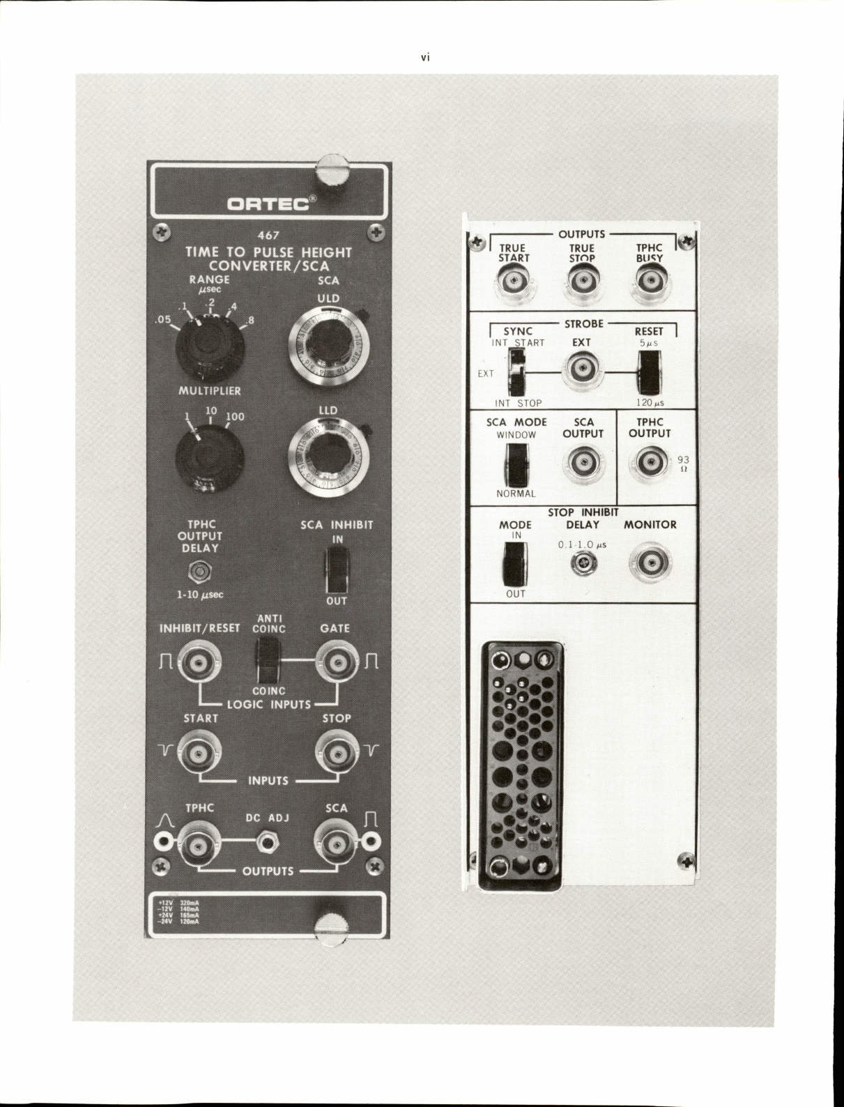
SCA
INHIBIT
IN
OUTPUT
DELAY
INHIBIT/RESET
CO!
n<'o^
;
;
GOING
LOGIC
INPUTS
START
INPUTS
DC
ADJ
TRUE
START
OUTPUTS
TRUE
STOP
TPHC
Blicy
o
STROBE
SYNC
RESET
INT
START
EXT
EXT
-I
INT
STOP
SCA
MODE
SCA
WINDOW
OUTPUT
NORMAL
TPHC
OUTPUT
0
STOP
INHIBIT
MODE
DELAY
MONITOR
O.M.O
(iS
G)
our
••••<
mvjil
m.
y-r.vriv^-,
if
"W-
r
f
%
*■
■
•
V.
;
.
-.
-
w-
■■■■'■
Table of contents
Other ORTEC Media Converter manuals


Popular Media Converter manuals by other brands


H&B
H&B TX-100 Installation and instruction manual

Bolin Technology
Bolin Technology D Series user manual

IFM Electronic
IFM Electronic Efector 400 RN30 Series Device manual

GRASS VALLEY
GRASS VALLEY KUDOSPRO ULC2000 user manual

Linear Technology
Linear Technology DC1523A Demo Manual

Lika
Lika ROTAPULS I28 Series quick start guide

Weidmuller
Weidmuller IE-MC-VL Series Hardware installation guide

Optical Systems Design
Optical Systems Design OSD2139 Series Operator's manual

Tema Telecomunicazioni
Tema Telecomunicazioni AD615/S product manual

KTI Networks
KTI Networks KGC-352 Series installation guide

Gira
Gira 0588 Series operating instructions

Lika
Lika SFA-5000-FD user guide