manuals.online logo
Brands
  1. Home
  2. •
  3. Brands
  4. •
  5. Panasonic
  6. •
  7. Tuner
  8. •
  9. Panasonic ST-CH7L User manual

Panasonic ST-CH7L User manual

Other Panasonic Tuner manuals

Panasonic TY-FB8TA User manual

Panasonic

Panasonic TY-FB8TA User manual

Panasonic WJ-ND300 Administrator Console User manual

Panasonic

Panasonic WJ-ND300 Administrator Console User manual

Panasonic WJ-NX400K User manual

Panasonic

Panasonic WJ-NX400K User manual

Panasonic WJND200 - NETWORK DISK RECORDER User manual

Panasonic

Panasonic WJND200 - NETWORK DISK RECORDER User manual

Panasonic CY-DAB2000N User manual

Panasonic

Panasonic CY-DAB2000N User manual

Panasonic WJ-ND300A User manual

Panasonic

Panasonic WJ-ND300A User manual

Panasonic WJND400 - NETWORK DISK RECORDER User manual

Panasonic

Panasonic WJND400 - NETWORK DISK RECORDER User manual

Panasonic WJND200 - NETWORK DISK RECORDER User manual

Panasonic

Panasonic WJND200 - NETWORK DISK RECORDER User manual

Panasonic WJ-NX300K User manual

Panasonic

Panasonic WJ-NX300K User manual

Panasonic WJ-ND300 Administrator Console User manual

Panasonic

Panasonic WJ-ND300 Administrator Console User manual

Panasonic TY-FB9TU User manual

Panasonic

Panasonic TY-FB9TU User manual

Panasonic TU-PTA500U User manual

Panasonic

Panasonic TU-PTA500U User manual

Panasonic WJ-ND300A/G Manual

Panasonic

Panasonic WJ-ND300A/G Manual

Panasonic WJ-ND300 Administrator Console Manual

Panasonic

Panasonic WJ-ND300 Administrator Console Manual

Panasonic WJ-NV300K User manual

Panasonic

Panasonic WJ-NV300K User manual

Panasonic WJ-ND300 Administrator Console User manual

Panasonic

Panasonic WJ-ND300 Administrator Console User manual

Panasonic WJND400 - NETWORK DISK RECORDER User manual

Panasonic

Panasonic WJND400 - NETWORK DISK RECORDER User manual

Panasonic WJ-NX200K/G User manual

Panasonic

Panasonic WJ-NX200K/G User manual

Panasonic TY-42TM6MA User manual

Panasonic

Panasonic TY-42TM6MA User manual

Panasonic WJ-VPU4000 User manual

Panasonic

Panasonic WJ-VPU4000 User manual

Panasonic WJND200 - NETWORK DISK RECORDER User manual

Panasonic

Panasonic WJND200 - NETWORK DISK RECORDER User manual

Panasonic WJ-NX400G-54000T6 User manual

Panasonic

Panasonic WJ-NX400G-54000T6 User manual

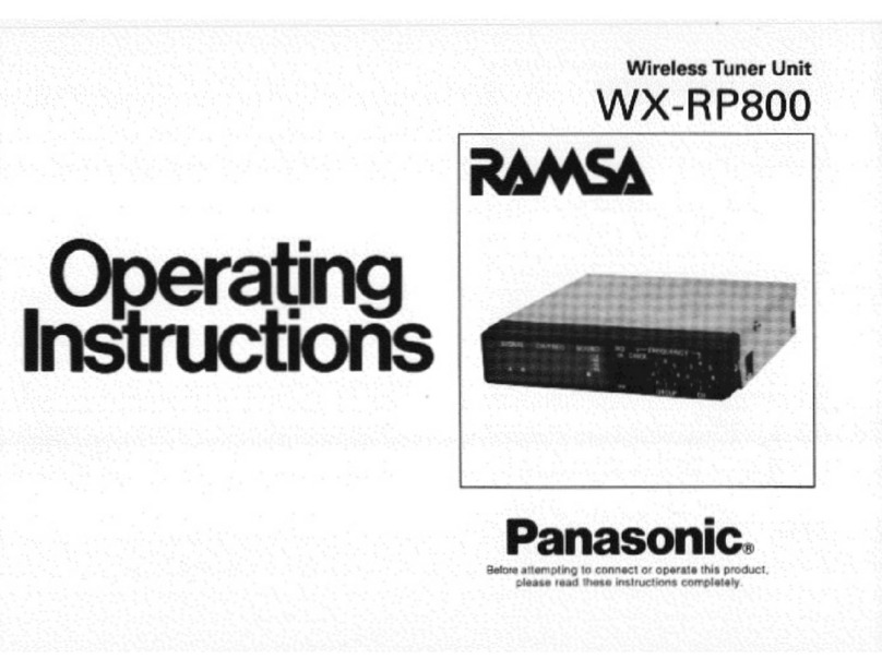
Panasonic Ramsa WX-RP800 User manual

Panasonic

Panasonic Ramsa WX-RP800 User manual

Panasonic WJ-NX200G User manual

Panasonic

Panasonic WJ-NX200G User manual

Popular Tuner manuals by other brands

Technics ST-HD55 Service manual

Technics

Technics ST-HD55 Service manual

Arcam DT91 Handbook

Arcam

Arcam DT91 Handbook

HDHomeRun 20121008 installation instructions

HDHomeRun

HDHomeRun 20121008 installation instructions

Eico HFT-92 instruction manual

Eico

Eico HFT-92 instruction manual

MFJ MFJ-928 instruction manual

MFJ

MFJ MFJ-928 instruction manual

Teac T-1D Service manual

Teac

Teac T-1D Service manual

NAD C 445 owner's manual

NAD

NAD C 445 owner's manual

Sony ST-SA5ES operating instructions

Sony

Sony ST-SA5ES operating instructions

Pioneer GEX-P700DAB Operation manual

Pioneer

Pioneer GEX-P700DAB Operation manual

Sirius Satellite Radio SC-FM1 user guide

Sirius Satellite Radio

Sirius Satellite Radio SC-FM1 user guide

Antique Automobile Radio 283501B Installation and operating instructions

Antique Automobile Radio

Antique Automobile Radio 283501B Installation and operating instructions

Sanyo FMT M15L Service manual

Sanyo

Sanyo FMT M15L Service manual

Monacor PA-1200R instruction manual

Monacor

Monacor PA-1200R instruction manual

Technics ST-X301L Service manual

Technics

Technics ST-X301L Service manual

Manhattan 176156 user manual

Manhattan

Manhattan 176156 user manual

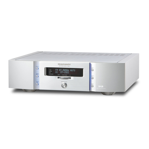
Marantz ST-15S1 user guide

Marantz

Marantz ST-15S1 user guide

Korg HA-40 owner's manual

Korg

Korg HA-40 owner's manual

Pioneer XC-IS21T Service manual

Pioneer

Pioneer XC-IS21T Service manual

manuals.online logo
manuals.online logoBrands
  • About & Mission
  • Contact us
  • Privacy Policy
  • Terms and Conditions

Copyright 2025 Manuals.Online. All Rights Reserved.

ORDER
NO.
AD9104083C8
Service
Manual
LW/MW/FM
Stereo
Tuner
Tuner
Color
(K)
e250
inf
Black
Type
Areas
Country
Code
(E)
Continental
Europe.
Asia,
Latin
America,
Middle
Near
East
and
Africa.
Because
of
unique
interconnecting
cables,
when
a
component
requires
service,
send
or
bring
in
the
entire
system.
Oceania.
System:
SC-CH7
@
SPECIFICATIONS
(DIN
45
500)
Sensitivity
(S/N
20
dB)
MW
20
uV,
300
pV/m
m@
FM
TUNER
SECTION
LW
50
pV
Frequency
range
87.50~108.00
MHz
(0.05
MHz
step)
Selectivity
(+9
kHz)
Sensitivity
1.5
uV
(IHF,
usable)
MW
(at
999
kHz)
50
dB
S/N
30dB
1.5
wV
(75Q)
LW
(at
216
kHz)
50
dB
S/N
26
dB
1.3
pV
(75Q)
S/N
20dB
1.2
pV
(75Q)
m
TIMER
SECTION
IHF
46
dB
stereo
quieting
sensitivity
28
pV
(750)
Clock
Quariz-lock
type
Total
harmonic
distortion
24-hour
indication
MONO
0.2%
Functions
24-hour
programmable;
STEREO
0.3%
weekly
(1
time)
S/N
once
only
(1
time)
MONO
60
dB
(74
dB,
IHF)
sleep
(1~120
min.,
1-min.
intervals)
STEREO
58
dB
(70
dB,
IHF)
Setting
intervals
1
minute~23
hours,
59
minutes
Frequency
response
20
Hz~15
kHz,
+0.5
dB~—1.5
dB
(at
1
min.
intervals)
Alternate
channel
selectivity
+400
kHz
50
dB
Stereo
separation
1
kHz
40
dB
@
GENERAL
10
kHz
30
dB
Power
consumption
8W
Channel
balance
(250
Hz~6,300
Hz)
+1.5dB
Dimensions
(WxHxD)
215x55x295
mm
Limiting
point
1.2
UV
(815/s2"
x
252"
x
115%")
Bandwidth
Weight
1.4kg
(3.0
Ib.)
IF
amplifier
180
kHz
FM
demodulator
1000
kHz
Notes:
Antenna
terminal
75Q
(unbalanced)
1.
Total
harmonic
distortion
is
measured
by
the
digital
spectrum
analyzer.
@
LW/MW
TUNER
SECTION
2.
Specifications
are
subject
to
change
without
notice.
Frequency
range
3.
Weight
and
dimensions
shown
are
approximate.
MW
522~1611
kHz
(9
kHz-step)
530~
1620
kHz
(10
kHz-step)
LW
144~288
kHz
(9
kHz-step)
146~290
kHz
(+2
kHz-shift)
System
[Tuner
|
—sAmplifier_—_—|
CD
Player
Cassette
Deck
Speakers
SC-CH7
ST-CH7L
SU-CH7
SL-CH7
RS-CH7
SB-CH7
‘Technics
/Panasonic
(E)
(GC)
(GN)
ST-CH7L
m@
CONTENTS
Page
LOCATION
OF
CONTROLS
...........
0.00
0c
cece
e
eee
eens
2,3
DISASSEMBLY
INSTRUCTIONS
................000
000
eee
4
MEASUREMENTS
AND
ADJUSTMENTS
..................
5,6
DESCRIPTION
OF
FLPANEL
...............000cceeeeeees
7
FUNCTION
OF
IC
TERMINALS..............0.00.0
00.
ce
ees
8
SCHEMATIC
DIAGRAM
..............000
cc
ccc
eee
e
eee
9~12
Note:
Page
PRINTED
CIRCUIT
BOARDS
AND
WIRING
CONNECTION
DIAGRAM
(.,
55355
05te
chen
fon
oi
wate
Saitonae
nae
oe
13,
14
BLOCK
DIAGRAM
..........0..
00.
c
cece
eee
e
eee
15,
16
REPLACEMENT
PARTS
LIST
..................0.000,
17~21
CABINET
PARTS
LOCATIONS
............0
0000
cece
cee ues
21
Refer
to
the
service
manual
for
Model
No.
SU-CH7,
Order
No.
AD9104082C8
for
information
on
ACCESSORIES,
INSTALLATION
OF
THE
SYSTEM,
CONNECTIONS
and
PACKAGING.
m@
LOCATION
OF
CONTROLS
SENSOR
CANCEL
RECALL
CLOCK
SET
WSELECT
A
©
Oo
G
STEREO
SYNTHESIZER
TUNER
ST-CH7L
om
MWV
ALLOCATION
PT
LW
FREQ
sine
PRESET
Tuner:
control
section
@
Timer
set
button
(TIMER
SET)
This
button
is
used
when
making
the
timer
setting.
Timer
select
buttons
(WV
SELECT
A)
These
buttons
are
used
when
setting
the
time.
And
when
making
the
timer
setting,
to
select
the
type
of
timer
operation,
the
day,
the
time,
etc.
@®
Remote
signal
sensor
(SENSOR)
Band
select
button
(BAND)
This
button
is
used
to
select
either
the
MW,
LW
or
FM
band.
Preset-tuning
buttons
(V
PRESET
A)
These
buttons
are
used
to
select
channel
numbers
for
a
broadcasting
station
which
has
been
stored
in
the
tuner’s
memory.
®
®
©
Timer
cancel
button
(CANCEL)
This
button
is
used
to
cancel
the
timer
setting.
Power
“STANDBY
()/ON”
switch
(POWER
STANDBY
(!)
/ON)
This
switch
switches
ON
and
OFF the
secondary
circuit
power
only.
The
unit
is
in
the
“standby”
condition
when
this
switch
is
set
to
the
STANDBY
('
position.
Regardless
of
the
switch
setting,
the
primary
circuit
is
always
“live”
as
long
as
the
power
cord
is
connected
to
an
electrical
outlet.
@
©
Timer
setting
confirmation
button
(RECALL)
This
button
is
used
to
confirm
the
timer
setting.
Clock
set
button
(CLOCK
SET)
This
button
is
used
to
set
the
present
time.
Memory
button
(MEMORY)
This
button
is
used
when
presetting
broadcast
station
frequencies
into
memory.
Tuning
buttons
(V
TUNING
A)
These
buttons
are
used
for
tuning
the
desired
broadcast
Station.
@ ©
@
SENSOR
ST-CH7L
Tuner:
display
section
@
©
©
86
®
&®
@®
Timer
play/recording
indicator
(PLAY,
REC)
This
indicator
shows
that
timer
play
mode
or
timer
recording
mode
is
activated.
Timer
mode-indicator
(]
ONCE,
WEEKLY)
This
indicator
shows
the
timer
operation
mode
(ONCE
or
WEEKLY).
Day
display
(SUN—SAT)
This
display
shows
the
present
day,
or
the
day
the
timer
has
been
set
for,
if
used.
Sleep
indicator
(SLEEP)
llluminates
when
the
sleep
timer
is
activated.
Timer
ON/OFF
indicator
(ON,
OFF)
This
indicator
shows
whether
the
times
for
timer
switch-ON
and
switch-OFF
have
been
set.
Time
display
This
display
shows
the
present
time,
or
the
time
the
timer
has
been
set
for.
FM
stereo
indicator
(STEREO)
This
indicator
automatically
illuminates
when
an
FM
stereo
broadcast
is
being
received.
It
will
not
illuminate
if
the
FM
mode
button
is
used
to
select
monaural
mode.
®
®
O08
8
O
Band
indicator
(FM,
MW,
LW)
Illuminates
to
show
which
band
is
selected.
Digital
frequency
display
Displays
the
broadcast
frequencies.
Quartz
lock
indicator
(QUARTZ
LOCK)
This
indicator
illuminates
when
the
unit
is
precisely
tuned
to
a
broadcast
station.
Memory
indicator
(MEMO)
This
indicator
illuminates
when
the
memory
button
is
pressed.
Preset
channel
display
This
display
shows
the
channel
number
selected
by
the
preset-tuning
buttons.
FM
mode
indicator
(AUTO,
MONO)
When
FM
broadcasts
are
being
received,
usually
the
“AUTO”
indication
is
illuminated.
When
the
FM
mode
is
set
to
monaural,
“MONO”
illuminates.
ST-CH7L
m@
DISASSEMBLY
INSTRUCTIONS
“ATTENTION
SERVICER”’
Some
chassis
components
may
have
sharp
edges.
Be
careful
when
disassembling
and
servicing.
aa]
Removal
of
the
Cabinet
1
Remove
the
5
screws
(@~@).
Procedure
1523
Pee
||
Removal
of
the
Operation
P.C.B.
Front
Panel
Reinforce
plate
1.
Remove
the
2
screws
(@, @).
1.
Puilup
the
position
©
of
the
front
panel
in
the
direction
of
the
2.
Remove
the
front
panel
in
the
direction
of
arrow.
arrow
@,
and
then
remove
the
reinforce
plate
in
the
direction
of
the
arrow
©.
*Remove
the
8
screws
(@~@).
ST-CH7L
ST-CH7L
m
MEASUREMENTS
AND
ADJUSTMENTS
This
TUNER
(ST-CH7L)
is
powered
by
the
amplifier
(SU-CH7).
To
adjust
it
or
check
operations
as
a
separate
unit,
follow
the
steps
below.
1.
Apply
a
power
supply
voltage
of
AC
23
V
to
[yZe
and
iZey)-
2.
Power
supply
switch:
ON
HOW
TO
CONNECT
Note:
Apply
a
power
supply
voltage
of
AC
23
V
to
pieydehd
and
paeygeyy
by
using
a
Voltage
Controller.
If
itis
not
available,
use
a
Power
Supply
Fixture
(SZZA1058C)
Voltage
controller
Power
Supply
Fixture
(SZZA1058C)
OR
instead.
©
a
e
ADJUSTMENT
POINT
AM
LOOP
ANT
AM
ANT
FM
ANT
TO
AMP
750
7
Z202
LINE
OUT
LINE
OUT
(Leh)
(Reh)
FM
mono
distortion
FM
offset
PLL
clock
Frequency
FM
MPX
VCO
(I9kHz)
eFM
ADJUSTMENT
Control
positions
and
equipment
used
@FM
signal
generator
(FM-SG)
Frequency
counter
Choke
coil
(100
LH)
e
Resistor
(100
kQ)
Stereo
modulator
e
Distortion
analyser
DC
electronic
voltmeter
(EVM)
Note:
For
Z201
(AM
ANT
and
OSC
coil),
Z202
(AM-IFT),
they
are
supplied
as
adjusted
parts.
So,
do
not
turn
the
cores
of
the
parts.
If
is
not
necessary
to
adjust
the
AM
circuit.
FM
OFFSET
VOLTAGE
AND
MONO
DISTORTION
ADJUSTMENT
FM
SIGNAL
GENERATOR
CONDITION
Modulation
1.
Test
equipment
connection
is
shown
in
figure.
Modulation
frequency
.
Set
the
unit
to
“FM”
mode.
Output
level
.
Set
the
radio
frequency
display
and
signal
generator
to
100.10
MHz.
.
Adjust
the
core
of
T201
so
that
the
voltage
measured
in
signal
mode
is
0
mV
(0+20
mV)
in
300
mV
range.
.
Adjust
T202
so
that
the
distortion
factor
of
L-CH
and
R-CH
is
minimized.
.
Repeat
steps
4
and
5.
Note:
The
adjusting
screwdriver
used
should
be
made
of
resin.
FM
MPX
VCO
ADJUSTMENT
.
Test
equipment
connection
is
shown
in
figure.
.
Set
the
unit
to
“stereo”
position.
.
Set
the
radio
frequency
display
and
signal
generator
to
100.10
MHz.
.
Adjust
VR501
for
19
kKHz+30
Hz
on
frequency
counter
reading.
FM
ANT
(759)
USING
ALTERNATE
SYSTEM
1.
Receive
the
stereo
broadcast.
2.
Adjust
VR301
until
stereo
indicator
lights
up.
Fix
the
arm
of
VR301
as
shown
in
gifure.
“Stereo”
FM
SIGNAL
GENERATOR
CONDITION
Modulation
Modulation
frequency
....
OkHz
Output
level
.
“Stereo”
OFF
position
.
“Stereo”
ON
position
(Indicator
lighting)
Adjust
point
of
pilot
circuit
PLL
CLOCK
FREQUENCY
ADJUSTMENT
Use
a
high
impedance
probe.
Frequency
counter
1.
Test
equipment
connection
is
shown
in
figure.
2.
Adjust
CT101
for
2070+0.010
kHz
(2050+0.010
kHz...GC
only)
on
frequency
counter
reading.
9
O00000
’
=
“requency
counter
*)
1
a
sis
circuit
requency
counter
(ar)
i
As
ST-CH7L
m@
DESCRIPTION
OF
FL
PANEL
[FL901
(RSLO096-F)]
eGRID
ASSIGNMENT
7G
SUN
MON
TUE
WED
THU
FRI
SAT
ONCE
WEEKLY
PLAY
REC
SLEEP
QUARTZ
LOCK
20
1
kHz
Memo
2alé
chsh
auto
cH.el_lé
el_le
@PIN
CONNECTION
3/3l2l2f2j/2t2;2l2j2i2l2ajiliaiaiatiasaia}ata}a
PIN
NO.
110/9/8/7/6/5/4/3/2/1]/o0/9/81/7/6/5/4/3/2]/1]ol9;8|7\/6/5/4/3]/2]1
FIF
P|P/P/P/PIP|P|Pj/P/P|PIP|P|P|P|P|P
N/FIE
CONNECTION
qiq}qtatadd
1IN/1/2/3/4/5/6/7
2/2
7/5/4/3/2]1lol9lslol1j2i3l4islel6élcialalalalaiala/pi1]41
Note:
1)
F1,F2..............
Filament
2)
INP
cricstsacicdta
Siateboestr
No
pin
3)
1G~8G
............
Grid
@
ANODE
CONNECTION
AM
—
PM
2e
FM
2e
|
2e
WEEKLY
2c
2c
_ _
2g
MW
29
ONCE
—
of
—
2t
2f
—_
2b
2b
—
2b
2b
+
=
i
a
2a,
2d, 2e,
2g
2a
STEREO
2a
2a
PLAY
ON
col
$1
2h
2h
2d
2a, 2d,
2e,
2g
AUTO
QUARTZ
LOCK
P8
WED
1d
1d
P9
SAT
le
le
P10
in
TUE
1c
1c
i
Pit
FRI
1g
1g
P12
MON
zi
1f
P13
THU
1b
P14
SUN
la
Pts
nn
P16
-_
—
ST-CH7L
m
FUNCTIONS
OF
IC
TERMINALS
@|C901
(MN187125STT1)
——
Pin
He)
:
Pin
Vo
:
No.
Mark
Division
Function
No.
Mark
Division
Function
1
VDD
I
Power
supply
(+B)
22
SBT1
O
Clock
terminal
for
serial
data.
:
OSCE
Connected
to
crystal
oscillator
23
CE
ie)
aie
Hensiniesion
Operation
(X901)
(4.19
MHz)
ip
enable
terminal
3
Osc
O
:
24
SBO1
ie)
Serial
data
signal
output
Connected
to
ground
terminal
BoC
OUE
2
External
control
clock
signal
input-
output
Connected
to
ground
terminal
26
|
CLOCKIN
X0
Not
connected
DATA
OUT
External
control
data
signal
output
7
KEY2
I
Key
scan
signal
input
Not
connected
8
|
KEY1
BIN
I
Connect
to
ground
terminal
a
I
Connectd
to
ground
terminal
9
CR
|
Not
connected
-——————_-—-—
sch
OT
DATA
IN
|
External
control
data
signal
input
Stereo
input
10
STEREO
I
Inputs
when
stereo
signal
receipt
Input
for
stop
signal
during
auto
“L”,
monaural
signal
receipt
“‘H”’.
tuning.
—S
Stops
auto
tuning
at
high
level.
When
broadcasting
receipt
“L”,
Receipt:
H,
No
signal:
L
14
DIR
|
stereo/normal
broadcasting
receipt
“H”.
Output
for
erasing
shock
noise
Not
connected
when
lock-off
at
PLL.
bt}
<Muting
outut>
12
MONO
oO
Auto/mono
change
over
terminal.
1.
Power
switch
“off”.
2.
Frequency
change
13
MERO
O
Remote
control
signal
terminal.
(up/down,
FM<—>AM<—>
TV)
14
Not
connected
Put
out
“H”
when
those
of
above
two.
15
INT
|
Remote
control
input
16
peas
l
Power
supply
level
detection
Netcoanecied
oe
DTS
selective
output
terminal.
.
oO
Key
scan
signal
output
wt
Not
connected
BM
AC
output
Put
out
for
“H’”
when
moving.
For
Digit
signal
output
to
FL
display
cutting
relay
dirive
of
main
power
3
POWER
o
supply.
Becomes
“H”
when
PLL
is
moving.
Reverse
when
put
the
power
key.
20
TB
I
Band
data
input
Reset
signal
input
21
RESET
l
Input
of
reset
for
micro
computer
stand
Serial
data
signal
input
Segment
signal
output
to
FL
display
FL
motor
power
supply
|
SCH
EMATIC
DIAG
RAM
(Parts
list
on
pages
17~20.)
Notes:
eS901,902
:
Preset
channel
switch.
(S901:
Up,
S902:
Down)
eS903
:
Band
select
switch.
eS904
:
Memory
switch.
eS905,
906
:
Tuning
switch.
(S905:
Up,
S906:
Down)
eS907,908
:
Timer
select
Switch.
(S907:
Up,
S908:
Down)
eS909
:
Timer
set
switch.
@S910
:
Clock
set
switch.
eS9i1
:
Timer
setting
confirmatin
switch.
e$912
:
Timer
cancel
switch.
eS913
:
Power
switch.
indicated
voltage
values
are
the
standard
values
for
the
unit
measured
by
the
DC
electronic
circuit
tester
(high-impedance)
with
the
chassis
taken
as
standard.
Therefore,
there
may
exist
some
errors
in
the
voltage
values,
depending
on
the
internal
impedance
of
the
DC
circuit
tester.
(_
):
MW
voltage,
[
]:
LW
voltage,
]:
MUTING
voltage
eimportant
safety
notice
Components
identified
by
A.
mark
have
special
characteristics
important
for
safety.
When
replacing
any
of
these
components,
use
only
manufacturer's
specified
parts.
eThis
schematic
diagram
may
be
modified
at
any
time
with
the
development
of
new
technology.
ooo00f
FMOSC
muaep
AMOSC
«Caution!
a>
IC
and
LSI
are
sensitive
to
static
electricity.
Secondary
trouble
can
be
prevented
by
taking
care
during
repair.
AM
signal
AF
signal
lines
*Cover
the
parts
boxes
made
of
plastics
with
aluminum
coil.
*Ground
the
soldering
iron.
*Put
a
conductive
mat
on
the
work
table.
«Do
not
touch
the
legs
of
IC
or
LSI
with
the
fingers
directly.
Positive
voltage
lines
--=—=—
Negative
voltage
lines
c—>
FM
signal
ST-CH7L
ST-CH7L
(o1ve
(04V1
Z101
FM
FRONT
END
PACK
(RALOOO6)
aa
f
1
wor
8
—
;
2SK544F-AC
2SC2786MKTA
ms
-
a
=
uKIO!
FM
stant
FM-RESAME
2.2P
PURI
ER
get
ss
8
~~
FM +B
LINE
TP
205
;
F201
coord]
BFP
gaa
$8
crz00
TP206
°
R252
8.2K
Al
FM
ANT
a
©:
mt
Ore
ane
Sa
ft
Se
a
;
aay
oe
al
ot,
Ce
onset
fi
"
-
TZ
ge
Se)
aT:
=
isev]KSAI75YGTA,,
earl.
See
paca
3
Jory,
202
Sad
8
:
22st
rrr
r
TK7Gi
7A
.
L-@--F
awe
ary
jan--@-4
ESR
EBT
SE
Sev
|
SWITCHING,
ANT
Ww
OSC
1
FM
ANT
G
1
le
ap
0201
(o1V)
FO)
ca
‘
C6
i3f
4
+
sf
44
I
)
1
LO.1V}
LO.IV)
2
O
(6.5
a
gt
Y!
?
e
|
1
4
R237
150,
PLL
clock
}qas1
O-7vo
j2)
8
48
Ati,
2
S15
C10
\
bp
|
LennY)
3
3
brequensy.
cee
()
2
lg
hI
)
S
adj.
°
?
:
L
4
ae
3
icin
C6)
(1.20)
\&
j
t==—-4
z
aero
gieen
pan
ox
Q201,
202
(1.6)
(OV)
q
For(GC,GN}
areas,
3
2SC2787LTA
peace
OV
n
obcg
|
p----.,
3
LL
FREQUENCY
VSS PD2
PD1
VOD2
VDDI
FM
IN/AM
IN|
LW
T
Te).
AM
(LW/MW)
FM
CLESAME
SYNTHESIZER
OB
f
i88
a
signal
ome
4
JKIO!
:
os
tivity
x
}
b=a-a=4
am
ant
CS)
i
FM
OSC
=
i
ee
L202
L
R211
C226
ff
je&
L------~
‘amie
WK
0.22UH
i
ato
at
680K
J18P
'
IW
he
—
Sore
ae
ave
|
(ov)
Ov.
a252
|
ov
(8.
AM
t
Lge
.
(ov)
Or
(om
£0
LOOP
AN
|
~10.22UH
xs
9257
R253
(OV)
Reese
og
Ul
3
0
I
|
1.8K
(J
SS
QF
C101
R106
"27
R262 6252
eal
=
:
S|
25v4.7
$60
S)
303«
Sovi
ae
=
&
:
"5,
—-
:
R104
aies
|
ee
=
|
a
19204
o—-—~$-WNro
pei
ae
S
0257
webb
PLL
clock
asl
0252
~254
¥.
Qio2
CH
KSC
2785YGTA
=3é
frequency
Dod
2s,
KSC2785YGTA
|
(eM)
% :
2s
|
(Dx
mek
:
|
BUFFER
AMP(LW/MW
OSC)
=
LW/MW
SWITCHING
jo
av
lw.
sot
se
y
|
set
By
38
6.1V
rok
|
'
N
X
Biv
tee
:
SY
(Mw
Yo
tw
Weta
tenet?
Q101,102
Q255,
256
es
sev}
a
59V
aay
;
&¢
SMH7
=
=
108MHz
2SC2785FETA
2SC2785FETA
x5l
|
|
eth
'
‘
FM
LOOP
FILTER
LW/MW
5g
'
aa
Fecye
l
LOOP
FILTER
A
13
be
;
OV
baw”
\
\
foes
a
cM
des
At
ono
ins
A
MAIN
CIRCUIT
530KH2
=e
1
6200K2
lageny
we
Dae
nh
R939
R938
R937
oN.
39
56
82
53
pReseyPas
|
ta
TONING)
:
«oy
Ate"
_
a
S206
Nar)
oy
s+
4
OTAI44ESTP
tees
Soot
|
food
;
SWITCHING
(PRESET
W)
|
(MEMORY)
|(
¥
TUNING)
|
(REMOTE)
8
g
sof
pend
Js
|
NAY
oy
r
a
We
i
2
sos,
i
FS
19MHz
Hl
|
|
Si
|
x
sf
y
2
59
&
on
@| 2]
2
a
|
'
2
2
'
|
or
$8
Fi
Pa
f\Ni
es
7
perce
»
vy?
|
al
F24
19MHz
uu
—
[—o*
o
rh
Tt
[be
3
ite
ale
eae
eas
x
Ekg
=
a
|
ase
338°
|
tog
TT
4
al
5
>]
8
BSe
BES
Sole
Ze
2
e901
oy
es
2.
z-
S
Shh
ee
Z|
zl
>
TS
S|
os},
SAY,
at
3 >
>} +)
=
pe
2
>|
>
2
=]
=} =]
af
so]
=
st}
ml
>
els
Nov!
oe
ee
a
eae
LG
et
Sl
eS
all
al
ele
3]
3h
3
pew
GS)
(9-H)
[
q
MONO
POWE!
q
Q90!1
KSC
2785
SWITCHING
(a
seugct)
{CLOCK
SET)
:
(RESET)
9
ea
|?
rT
Icg01
°
MNI87I2
MICRO
COMI
1.8K
@cse
(ee!
OPERATION
ace-278
CIRCUIT
(
REMOTE
SENSOR)
S15
$14
S13)
S12
$11
S10
s9
so
si
FL
901
(RSLOO96-F)
FL
OISPLAY
TEES,
as
T=
4ms
-~10—
>
—:
re
———
TP206
R252
8.2K
AM*B
LI
1c201
e260
aK
a
208-208
AN7273W
25!
8°
aM
iLwaaw
KSAII75YGTA
FM/AM
IF
AMP
(sev
KSA
II
75YGTA
te
Nose
POWER
SUERLY.
DETECTOR
e.av|
LW/MW
2.28
‘4
S
oy
|
SWITCHING
_
\
tas
r
"
\
ns
vy
Ov
You
SRY
teh
8
AI
of
0251
=
t
+
le)
46
J
teas
,
sp
48
at
E54
0209
ay)
bd
i
O.7V
C44)
x
Coen
ty
I
Ua7vi
fla
7VI
=
|
LW
ANT
L
eel
Q207
ry
xe
KSC2785YGTA
3
x
paren
2
ca
me
:
POWER
SUPPLY
CONT.
(ov)
OV.
Q252
0.6V
(8.87)
0.6V|
glx
Cov)
(0.7
COV]
ga54
R212
470K
Ber
R253
COV)
arn
1B
(02M)
=
es
28
£0.7v)
“Stitt
tH
=
-
t
9204
a
38
252
~254
KSC
2785YGTA
3
7
aes
KSC2785YGTA
SIGNAL
DETECTOR
z
5
8
LW/MW
SWITCHING
FM
offset
voltage
(O
mv)
ST-CH7L
ST-CH7L
FM
MPX
VCO
adi
(19OKHzZ
output)
FM
MPX
VCO
adj
5+
0302_1SS254TA
R314
1K
Q205
KSC
2785YGTA
=
SWITCHING
58:
&
0303,
304
3st
-
US
2SC1740SQSTA
R228
1C30l
2
iS
©
MUTING
100K
tov3
RVIBAI332L
%
I~
,
poe
ee]
CLBV}
|
(ove
FM
MPX
0
S
a
.
iSVil
264
gs
i
=
men
ee)
ea
8.
4y
Ss
“i
311
50V1
a
ELA
ae
eee
pes
Ny
‘7
ess
”
83
303
5
‘
=
at
9205
|.)
ay)
20K
£38
01
a
g
eae
joes
2
2
e
C17V}
srvfiev[sav[
~
Lévl.
evi!
ev
s
3
w0.01
FM
mono
7
bS
(3)
al
SB
i
‘as
/
distortion
ad)
§
8B
3
TS
ik
on
AF
signal
0.3V
sv
15.3V)
leg
|S
5
2.9V
PLL
=
a
|{DETH{AF_ANe
1202
p—iwex
F<
4
en
x
|
87s
'@
Sp
3
ease
vay
SS
8a
OX
[
3 8
C352,
16V10
o>
‘
c312
Sov
TE
Ba
@O—O)—(6)—B)
OD
3
cr
tans
T
:
*[
:
*
a
ie
sot
[yf
S4v[54vf0
avy
6v]
ov
Tey
ov
“4
°
ox
v
5
=
=
be)
58
8
BLS
b
©
7
R305
6.8K
Al
a|
a
a=
g
es
8
R301
ons
FM
offset
«je
4
3s
hoK«B)
R|
5
voltage
o
ba}
4
2
Q301,
302
(0
é
©
LJ
KSC
2785YGTA
MM
8
-
BUFFER
AMP
2
f
u
To
SL-CHT7/
SuU-CH7
901
100UH
£OO™
N902
(1/2)
cP902
(1/2)
53V
1SS254TA
CN902
(1/2)
1SS254TA
R914
e901
KSC
2785YGTA
SWITCHING
(RESET)
Ic90l
MNI87I25STTI
MICRO
COMPUTER
902,903
OTC
144
ESTP
BUS
LINE
DRIVE
ROIS
R915 C922
25v3.3
R928 4.7K
0903
1S8S254TA
907,908
KSC2785YGTA
POWER
DOWN
DETECTOR
39K
10
0904,
905
KSC2785YGTA
BUS
LINE
DRIVE
Q701
2S01862QRTVE6
REGULATOR
e}6
Bsk
is
=
gst
3
=
2
J
Bee
ns
+
9
=
3
560
=
=
he
B48
SS
Bas
=
=
MA4068MTA
!-5K
Aozos
AT
SR
35z00Te
ARTE
\
ov
0704
4
R712
5.6K
=@
thr
Q703
cba
t
ee
ue
KSC2785YGTA
SWITCHING
(POWER
CONT.)
At
1/2W
150,
a!
al
C708
S
ooora
|
Log
|
ST
ase
|
Sire
|
@!
Bos
re
R£S
5
!
ota
o
*
ac
san}
1
MA
4240MTA
C713
50V22
0712
D714 0716
0718
0711
D713 0715 0717
0711~718
1SS254TA
R710
100
0709
MA4O47MTA
R711
00
ora
50v1
Y q
R705,
2.2
C715
20.01
—
ST-CH7L
ST-CH7L
o
®
me]
2
GS
xe)
)
&
”
<x
<x
5
I
F<
ree.
rea
txt
*
5
LW
Or
E
EE
a
=
vi)
reg
a
OoOr
LO
=
>
©
0
oR
o>~>
ko
N
0
2
S
7
00
00
om
ow
tO
t
©
o
i
x
RR
FNROT
i
wo
OOo
©
Zz
a
NN
KRrtvt
NO
t+
=
<
S
OO
erates
nO
oo
txt
a
&
QQ
BODE
22
==
o
ara
ao
-_
°
@
oO
rr
<<
4
no)
ke
>
3G
|
ke
Es
re
<
£
Ee
©
>
n
2)
co
-
5
Le
8
x
Co
-
oo
3
=
ey
q
&
Page
£
©
2
cs)
ie
o
3
Bigg
E
z
@
Be
ee
NBs
o
=
nN
a
=
N
e
i
o%
8
So
x8
Copied
On
of
PS
=
re
soo
fp
=o
he
ae,
Loa
7.)
=
z
q
3
29
fa]
i
22
ad
e
a
ald
so
=
ee
<x
le
x
lela
Oo
alls|i
8)
2|2
J}
jala
<q
J
ltle
=a
Q!
2
i
QO
f2._|
z
Ca
Oo
/
nd
a7
e
<<
ey
haa
SEES
u
ro
i
ise
sees
Se
ae
Z
Snes
ot
er
rt
—-
riwetina
C.
eee
‘
za
=
oO
z
z5
OO
oO
Oo
44
a
nn
oO
E
z
\e)
S
z
>
r=
Eq
Oo
See
4
g
82
a
“i
Q
3
a8
<q
Agowaw
|
|
4—-ONINAL—V
|
Q
a
co
2
=
=
om
é
ma
q
a
_
uJ
a
5
bee
5
(13s
yawi.|[
4-19313S-¥
'YOSNAS
anve
|
a
=
a
|_|
<q
a
oO
[=]
Ww
ire
~14~
43
m@
BLOCK
DIAGRAM
ST-CH7L
ST-CH7L
—15—
~16—
(5
Pee
ees
JK7O
FM
MONO
DISTORTION
adj.
RMI
ALSS2E
0302
c
amp
eek
FM
MPX
D302
o
9
T201,202
ANT273W
1
A)
a304
FM
ANT
7;
7H
®
8
jet,
coi
zi0l
sea
FM/AM
IF
AMP.
DET
tt
FM
FRONT
END
CF201
CF
202
CB)
#
RFamp
Q201,202
5!
t
3 5
7
3
13
ete
|
C201
pds
ies
GND
|
I
1
|
1
=
<eqferere
|
!,
@205
BL
aVA
E>
y
i
:
n
in
1
CD
+
Ves
dt
4
|
Capen
ar}
|
i
ga
te
I
ees
|
aD
ee
ae
el
—<+
—<
|
12
14
6
8
sf
Tr
v4
16
TP3010
ib
gee
a
|
va
!
+
I
4
VR301
a
|
-——-
(FM
MPX
}
18 10
ts
;
cf
i
VCO
adj)
|
SSK
Buffer
(>
-
Q303
;
OQ)
Q256
Signal
receive
detector
XIOl
CTIO!
(72MHz)
D201
z901
LM7OOI
}
_
REMOTE
Spd7te3ds
Licio1)
CONTROL
~
PLL
FREQUENCY
control
SENSOR
(AM)
@B)
FM/AM
XOUT
XIN
LW
PD2
FMIN
SYNTHESIZER
Power
Supply

Shem
AM
IN
(FM)
GB)
Selector
Vss
TB
CE
CL
DATA
~
Fe
7
$3 94
FO
Switching
(reset)
|
907,908
KEY
MATRIX
20
|
23
24
31
21
32
10
12
bis
19
Aah
ae
So)
Shae
ee
Ses
Sh
ee
=f
cn
pe
eS
ae
=
Spa
eee
eee
a
se
ee
—
a
ny
eee
za
TB
CE
SBT!
sBol
spb
POWER
RST
MUTE
STEREO
MONO
INT
POWER
Q902~905
KEY2
DOWN
\(APRESET)
(ATUNING)
a
MNiaTIsSST
Ti
CLOCK
Our?
)
$901
$905
|
1c901
|
CLOCK
IN
©
\
I
|
2
JL
|
MICROCOMPUTER
DATA
OUTY
=
(WPRESET)
|
(MEMORY)
|
(Ww
TUNING)
|
(CONTROLLER)
DATA
Ind
—{6)
$902
$904
s906
|
|
SEGO
~
SEGI5,
P70
DGTO~DGT6
”*
Bs
xe
L.
_kS!_ks2_ks3__
osc2__osci
Vv
pp
|
ioe
ee
ePecae
aes
anne
N
en
rer
NN
i
ee
es
Se
|
z.
P
|
35
36
37
2
3
47
63 38
44 64
(BAND)
|
!
$903
31x
901
tt
ye
v
|
£
1
tOH
|
|
\
|
|
|
be
aa
|(
SELECT)
2
S907
4
A
Q703
0701,705
T701
|
p
FL
DISPLAY
l(w
SELECT)
(RECALL)
|
$908
soll
|
oO
oO
|
|
Da
A
we
<
—
a
(TIMER
SET)
(CANCEL)
|
(POWER)
|
$909
$912
See
|
p
p
p
|
|
Note
1
SSS
=
7A
4
Le
4
1
—P—:FMSIGNAL
|
ooot>
=
FM
OSC
&
D707
'AM
SIGNAL
|
®:
AM
OSC
i]
Rech
out
Lech
out
POWER
B.CLK
B.DATA
B.
GND
Ac
Ac