PIONEER DJ rekordbox XDJ-700 User manual

ORDER NO.
PIONEER CORPORATION 1-1, Shin-ogura, Saiwai-ku, Kawasaki-shi, Kanagawa 212-0031, Japan
PIONEER ELECTRONICS (USA) INC. P.O. Box 1760, Long Beach, CA 90801-1760, U.S.A.
PIONEER EUROPE NV Haven 1087, Keetberglaan 1, 9120 Melsele, Belgium
PIONEER ELECTRONICS ASIACENTRE PTE. LTD. 253 Alexandra Road, #04-01, Singapore 159936
Pioneer DJ Corporation 2015
2015 Printed in Japan
XDJ-700
RRV4637
MULTI PLAYER
XDJ-700
THIS MANUAL IS APPLICABLE TO THE FOLLOWING MODEL(S) AND TYPE(S).
THIS SERVICE MANUAL SHOULD BE USED TOGETHER WITH THE FOLLOWING MANUAL(S).
Model Type Power Requirement Remarks
XDJ-700 UXJCB AC 100 V to 240 V
XDJ-700 SYXJ AC 100 V to 240 V
XDJ-700 FLXJ AC 100 V to 240 V
XDJ-700 AXJ AC 100 V to 240 V
Model Order No. Remarks
XDJ-700 RRV4638SCHEMATIC DIAGRAM, PCB CONNECTION DIAGRAM, PCB PARTS LIST
K-MZV NOV.

2XDJ-700
12 3 4
A
B
C
D
E
F
12 3 4
SAFETY INFORMATION
WARNING
This product may contain a chemical known to the State of California to cause cancer, or birth defects or other reproductive
harm.
Health & Safety Code Section 25249.6 - Proposition 65
This service manual is intended for qualified service technicians; it is not meant for the casual do-it-
yourselfer. Qualified technicians have the necessary test equipment and tools, and have been trained
to properly and safely repair complex products such as those covered by this manual.
Improperly performed repairs can adversely affect the safety and reliability of the product and may
void the warranty. If you are not qualified to perform the repair of this product properly and safely, you
should not risk trying to do so and refer the repair to a qualified service technician.
1. SAFETY PRECAUTIONS
The following check should be performed for the
continued protection of the customer and service
technician.
LEAKAGE CURRENT CHECK
Measure leakage current to a known earth ground
(water pipe, conduit, etc.) by connecting a leakage
current tester such as Simpson Model 229-2 or
equivalent between the earth ground and all exposed
metal parts of the appliance (input/output terminals,
screwheads, metal overlays, control shaft, etc.). Plug
the AC line cord of the appliance directly into a 120 V
AC 60 Hz outlet and turn the AC power switch on. Any
current measured must not exceed 0.5 mA.
ANY MEASUREMENTS NOT WITHIN THE LIMITS
OUTLINED ABOVE ARE INDICATIVE OF A POTENTIAL
SHOCK HAZARD AND MUST BE CORRECTED BEFORE
RETURNING THE APPLIANCE TO THE CUSTOMER.
2. PRODUCT SAFETY NOTICE
Many electrical and mechanical parts in the appliance
have special safety related characteristics. These are
often not evident from visual inspection nor the protection
afforded by them necessarily can be obtained by using
replacement components rated for voltage, wattage, etc.
Replacement parts which have these special safety
characteristics are identified in this Service Manual.
Electrical components having such features are
identified by marking with a >on the schematics and on
the parts list in this Service Manual.
The use of a substitute replacement component which
does not have the same safety characteristics as the
PIONEER recommended replacement one, shown in the
parts list in this Service Manual, may create shock, fire,
or other hazards.
Product Safety is continuously under review and new
instructions are issued from time to time. For the latest
information, always consult the current PIONEER Service
Manual. A subscription to, or additional copies of,
PIONEER Service Manual may be obtained at a nominal
charge from PIONEER.
Leakage
current
tester
Reading should
not be above
0.5 mA
Device
under
test
Test all
exposed metal
surfaces
Also test with
plug reversed
(Using AC adapter
plug as required)
Earth
ground
AC Leakage Test
(FOR USA MODEL ONLY)

3
XDJ-700
56 7 8
56 7 8
A
B
C
D
E
F
CONTENTS
SAFETY INFORMATION.......................................................................................................................................................... 2
1. SERVICE PRECAUTIONS.................................................................................................................................................... 3
1.1 NOTES ON SOLDERING ............................................................................................................................................... 3
1.2 NOTES ON REPLACING PARTS ................................................................................................................................... 4
1.3 SERVICE NOTICE.......................................................................................................................................................... 4
2. SPECIFICATIONS................................................................................................................................................................. 5
3. BASIC ITEMS FOR SERVICE .............................................................................................................................................. 6
3.1 CHECK POINTS AFTER SERVICING ........................................................................................................................... 6
3.2 JIGS LIST ....................................................................................................................................................................... 6
3.3 PCB LOCATIONS ........................................................................................................................................................... 7
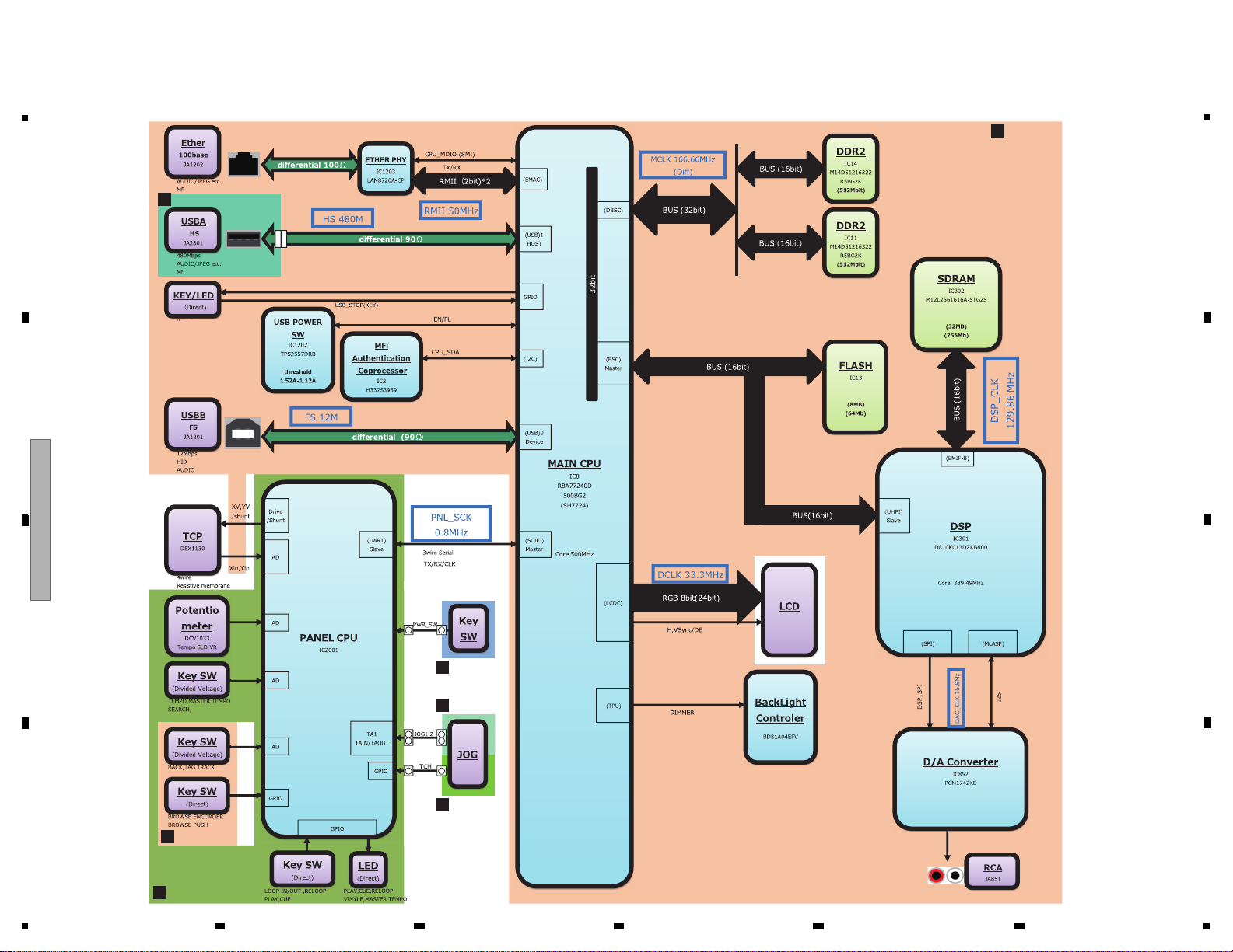
4. BLOCK DIAGRAM ................................................................................................................................................................ 8
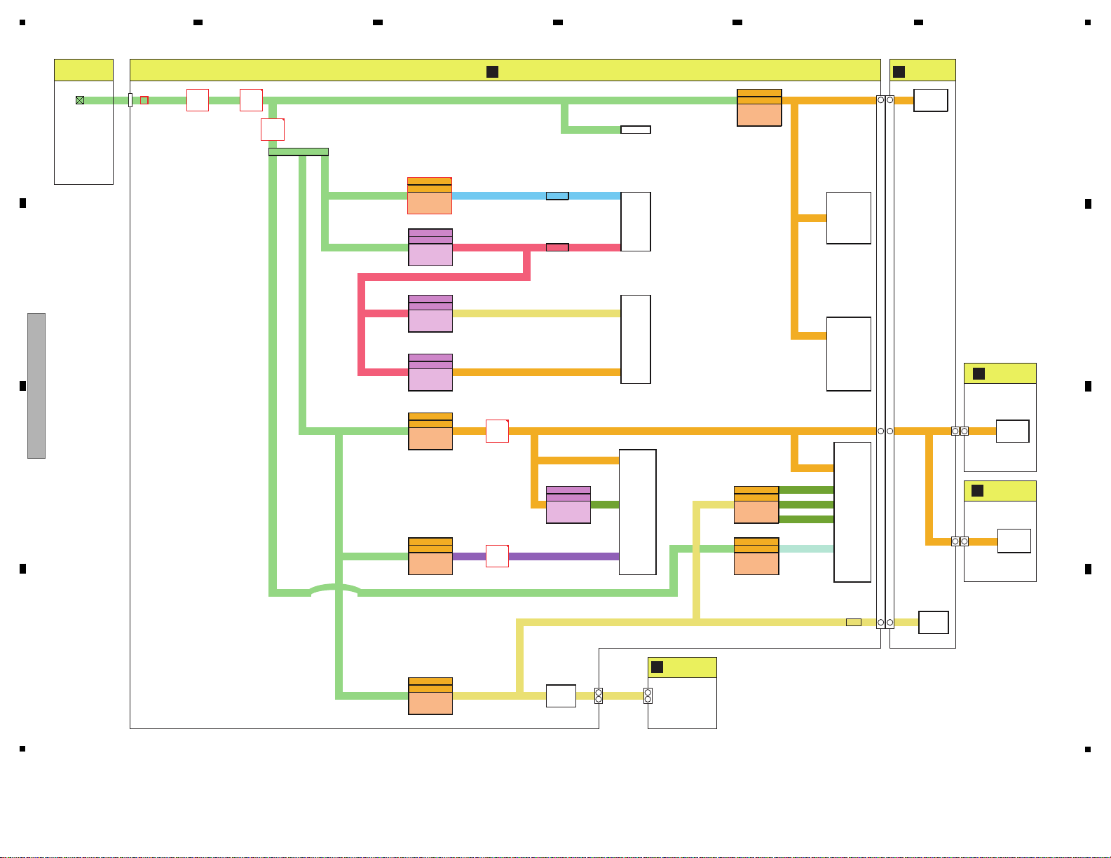
4.1 OVERALL WIRING DIAGRAM ....................................................................................................................................... 8
4.2 SIGNAL BLOCK DIAGRAM............................................................................................................................................ 9
4.3 POWER SUPPLY BLOCK DIAGRAM........................................................................................................................... 10
5. DIAGNOSIS ........................................................................................................................................................................ 11
5.1 POWER ON SEQUENCE............................................................................................................................................. 11
5.2 TROUBLESHOOTING.................................................................................................................................................. 12
5.3 CONNECTION CONFIRMATION WITH THE PC......................................................................................................... 20
6. SERVICE MODE................................................................................................................................................................. 21
6.1 SERVICE MODE .......................................................................................................................................................... 21
6.2 ABOUT THE DEVICE................................................................................................................................................... 29
7. DISASSEMBLY ................................................................................................................................................................... 30
8. EACH SETTING AND ADJUSTMENT ................................................................................................................................ 38
8.1 NECESSARY ITEMS TO BE NOTED........................................................................................................................... 38
8.2 FIRMWARE UPDATE / RECOVERY............................................................................................................................. 38
8.3 WRITING THE SERIAL NUMBER OF THE UNIT ........................................................................................................ 38
8.4 JOG DIAL ROTATION LOAD ADJUSTMENT ............................................................................................................... 39
8.5 ITEMS FOR WHITCH USERS SETTING IS AVAILABLE............................................................................................. 40
9. EXPLODED VIEWS AND PARTS LIST............................................................................................................................... 41
9.1 PACKING SECTION ..................................................................................................................................................... 41
9.2 EXTERIOR SECTION .................................................................................................................................................. 43
9.3 DISPLAY SECTION ...................................................................................................................................................... 45
9.4 JOG DIAL SECTION .................................................................................................................................................... 47
1. SERVICE PRECAUTIONS
1.1 NOTES ON SOLDERING
• For environmental protection, lead-free solder is used on the printed circuit boards mounted in this unit.
Be sure to use lead-free solder and a soldering iron that can meet specifications for use with lead-free solders for repairs
accompanied by reworking of soldering.
Do NOT use a soldering iron whose tip temperature cannot be controlled.

4XDJ-700
12 3 4
A
B
C
D
E
F
12 3 4
1.2 NOTES ON REPLACING PARTS
1.3 SERVICE NOTICE
The part listed below is difficult to replace as a discrete component part.
When the part listed in the table is defective, replace whole Assy.
Assy Name
MAINAssy Authentication Coprocessor H337S3959 USONpackage
(UltraSmallOutlineNon-lead)
IC2
DDR2 M14D51216322R5BG2K BGA packageIC11, 14
MAINCPU R8A77240D500BG2 BGA packageIC8
DSP D810K013DZKB400 BGA packageIC301
LCD Backlight Power IC BD81A04EFV-M IC with heat-padIC701
12 V→3.3 VDC/DC Converter BD9328EFJ IC with heat-padIC1301, 1302
12 V→1.2 VDC/DC Converter BD9328EFJ IC with heat-padIC1303
USBA Current Limit IC TPS2557DRB QFN, IC with heat-padIC1202
ETHER PHY LAN8720A-CP QFN, IC with heat-padIC1203
LCD Power IC R1290K103A QFN, IC with heat-padIC702
Parts that is Difficult to Replace
Ref No. Function Part No. Remarks
About the Flash ROM (IC13) in the MAIN Assy
Replacement of the Flash ROM (IC13) in the MAINAssy is not possible during service, because writing of the MAC address
on the production line is required.
Therefore, the Flash ROM (IC13) is not supplied as a service part. If the Flash ROM is defective, replace the whole MAINAssy.
After replacing the the MAINAssy, writing of the serial number of the unit is required.
For details on how to write the serial number, see "8.3 WRITING THE SERIAL NUMBER OF THE UNIT."
About backup of the UTILITY settings
As this unit is provided with user-settable UTILITY settings (such as the Play mode setting,) it is recommended that you back
up the settings before starting repair. The settings can be stored for backup in a USB memory device.
For details on how to back up and restore data, see "gHow to Back Up and Restore the Settings" in "8.5 ITEMS
FOR WHICH USER SETTINGS ARE AVAILABLE ."
About discharging
If the 29-pin flexible cable connecting CN2001 on the PNLB Assy and CN1103 on the MAINAssy of the control panel section
is disconnected, be sure to unplug the Power cord then wait 3 minutes or more before reconnecting the flexible cable.
This is because the internal electrical charge remains in the power circuit for a while after the Power cord is unplugged.
If the flexible cable is connected in such a state, L706 will be damaged.
If the ICP is damaged, no buttons or LEDs of the unit will light and nothing will be displayed when the POWER switch
is set to ON.
Control panel Section
• Bottom view
29-pin flexible cable MAINAssy
PNLB Assy
CN2001
CN1103

5
XDJ-700
56 7 8
56 7 8
A
B
C
D
E
F
2. SPECIFICATIONS
AC adapter
Power............................................. AC 100 Vto 240 V, 50 Hz/60 Hz
Rated current............................................................................0.6 A
Rated output.................................................................DC 12 V, 2 A
Power consumption (standby) ................................................0.5 W
General – Main Unit
Power consumption .............................................DC 12 V, 1200 mA
Main unit weight..........................................................2.0 kg (4.4 lb)
(When not attached with the stand)............................ 1.7 kg (3.7 lb)
External dimensions
............................. 238 mm (W) × 106.3 mm (H)× 307.8 mm (D)
(9.3 in. (W) × 4.1 in. (H) × 12.1 in. (D))
(When not attached with the stand)
............................... 238 mm (W) × 78.8 mm (H) ×307.8 mm (D)
(9.3 in. (W) ×3.1 in. (H) ×12.1 in. (D) )
Tolerable operating temperature..............................+5 °C to +35 °C
Tolerable operating humidity............5 % to 85 % (no condensation)
Analog audio output (AUDIO OUT L/R)
Output terminals ......................................................... RCA terminal
Output Level .......................................................... 2.0 Vrms (1 kHz)
Frequency response................................................. 4 Hz to 20 kHz
S/Nratio.................................................................................115 dB
Total harmonic distortion .....................................................0.003 %
USB downstream section (USB)
Port ........................................................................................ Type A
Power supply.............................................................5 V/1 A or less
USB upstream section (USB)
Port ........................................................................................ Type B
LAN (PRO DJ LINK)
Rating ...........................................................................100Base-TX
Main display
Display type.............. Active matrix TFT liquid crystal display (LCD)
Supported languages ................................................. 18 languages
• The specifications and design of this product are subject to
change without notice.
Accessories
• Power cord
(UXJCB: XDG3052)
(SYXJ: ADG1154)
(FLXJ: ADG1154, ADG7097)
(AXJ: ADG7079)
• Audio cable × 1
(XDE3045)
• LANcable × 1
(DDE1141)
• AC adapter × 1
(DWR1546)
• Operating Instructions (Quick Start Guide) × 1
(UXJCB: DRH1313)
(SYXJ: DRH1314)
(FLXJ: DRH1315)
(AXJ: DRH1316)

6XDJ-700
12 3 4
A
B
C
D
E
F
12 3 4
3. BASIC ITEMS FOR SERVICE
3.1 CHECK POINTS AFTER SERVICING
3.2 JIGS LIST
Items to be checked after servicing
To keep the product quality after servicing, confirm recommended check points shown below.
1Confirm the firmware version on Service mode. The version of the firmware must be latest.
Update firmware to the latest one, if it is not the latest.
2Confirm whether the customer complain has been solved. The customer complain must not be reappeared.
4Check output signals while the Jog dial or TEMPO slider is being
operated.
Audio and operations must be normal.
5Check the keys on the unit. Check whether a product can be operated properly by buttons
on the product.
6Check the LCD display.
Check that there is no dirt or dust trapped inside the LCD display.
7 Check the Touch panel.
Check whether a product can be operated properly in an all-black
screen of the Service mode.
Audio, Search and operations must be normal.
8
Check the appearance of the product.
No scratches or dirt on its appearance after receiving it for service.
3Check the connection of each interface.
Playback data contained in the device connected to USB A.
The PC must be linked.USB B.
The PC must be linked.LINK.
Distortion
Noise
Volume too low
Volume too high
Volume fluctuating
Sound interrupted
See the table below for the items to be checked regarding audio.
Item to be checked regarding audio
No. Procedure Check points
Lubricants and Glues List
Name Part No. Remarks
Lubricating oil GYA1001 Refer to "9.4 JOG DIAL SECTION".
Jigs List
Jig Name Part No. Purpose of use / Remarks
Software for writing the serial number GGS1177 For writing the serial number of the unit to the MAINAssy after replacement.
The zipped writing tool (mmpforseigi.exe) and data file (hidcom.dll) are
posted at Niis.
See "8.3 WRITING THE SERIAL NUMBER OF THE UNIT."

7
XDJ-700
56 7 8
56 7 8
A
B
C
D
E
F
3.3 PCB LOCATIONS
1..MAIN ASSY DWX3744
NSP 1..PNL ASSY DWM2581
2..PNLB ASSY DWX3745
2..JOGB ASSY DWX3746
2..TCHB ASSY DWX3747
2..PSWB ASSY DWX3748
2..USBA ASSY DWX3749
2..TXLB ASSY DWX3750
Mark No. Description Part No.
LIST OF ASSEMBLIES
NOTES:
-
Parts marked by “NSP” are generally unavailable because they are not in our Master Spare Parts List.
-
The >mark found on some component parts indicates the importance of the safety factor of the part.
Therefore, when replacing, be sure to use parts of identical designation.
F
PSWB ASSY
C
USBA ASSY
A
MAINASSY TXLB ASSY
• Bottom view
PNLB ASSY
B
JOGB ASSY
D
TCHB ASSY
E

8XDJ-700
12 3 4
A
B
C
D
E
F
12 3 4
4. BLOCK DIAGRAM
4.1 OVERALL WIRING DIAGRAM
AC ADAPTER
(DWR1546-)
*RIGHT ANGLE
*RIGHT ANGLE
FOR DEBUG (DSP&CPU)
AKN7115-A
TFT-LCD MODULE (CWX4352)
POWER CORD
Anode
Cathode
*RIGHT ANGLE
*HORIZONTAL
Part Number
ADG1154-
XDG3052-/UXJCB
DDG1112-
/AXJ
/SYXJ
/FLXJ
DESTINATION
/JXJ
ADG1154-
ADG7079-
(taiwan) ADG7097-
POWER CORD
Polarity
Non-Polarized
Use "megane" type
*HORIZONTAL
*VERTICAL
*HORIZONTAL
*HORIZONTAL
FPC 0.5mm Pitch 28mm
ASG1102-A
*VERTICAL
RL
TOUCH PANEL (DSX1130)
PF03PP-B17
L=175mm
B to B Connect
2.0mm Pitch
*HORIZONTAL
FPC
L=50mm
JP2001
D20PDY0320E
2.0mm Pitch
L=200mm
DDD1725-
FFC(SAME FACE)
L=100mm
Pitch=1.0mm
L=110mm
Pitch=2.0mm
Board in
DKB1118-A CKS4428-A
1BLACK
2
WHITE
CKS6646-A
ZIF
1
NC
2
GND
3
VGL
4
VCC
5
VGH
6
NC
7
V1
8
V2
9
V3
10
V4
11
V5
12
V6
13
V7
14
V8
15
V9
16
V10
17
NC
18
NC
19
DITH
20VCOM
21
AVDD
22
AGND
23
GND
24
UPDN
25
VCC
26
SHLR
27
STBYB
28
RSTB
29
MODE
30
VSD
31
HSD
32
DE
33
DCLK
34
B7
35
B6
36
B5
37
B4
38
B3
39
B2
40
B1
41
B0
42
G7
43
G6
44
G5
45
G4
46G3
47
G2
48
G1
49
G0
50
R7
51
R6
52
R5
53
R4
54
R3
55
R2
56
R1
57
R0
58
VCC
59
AVDD
60
AGND
DKN1237-A
VBUS
D-
D+
GND
CKS6625-A
1YT
2XR
3YB
4XL
DKB1114-A
DKN1649-A
DKP3864-A
1
GNDD
2
V+3R3
3
JOG1
4
JOG2
KM200NA4L
1GNDD
2V+3R3
3JOG1
4JOG2
CKS3561-A
1
V+5_USB
2
V+5_USB
3
USB_DN_A
4
GNDD
5
USB_DP_A
6
GNDD
CKS3533-A
1GNDD
2USB_DP_A
3GNDD
4USB_DN_A
5V+5_USB
6V+5_USB
KM200NA3L
1
GNDD
2
TCH
3
V+3R3
KM200NA3L
1GNDD
2JOG_SW
3V+3R3
VKN1260-A
CN2001
1
V+3R3E
2
GNDD
3
TCP_XIN
4
GNDD
5
TCP_YIN
6
GNDD
7
TCP_YV
8
KEY_1
9
TCP_XV
10
GNDD
11
ENC_2
12
ENC_SW
13
ENC_1
14
GNDD
15
PNL_CNVSS
16
XPWR_ON
17
EUPL
18
GNDD
19
PNL_RST
20
V+3R3
21
V_DET
22
GNDD
23
PNL_RXD
24
PNL_BUSY
25
PNL_TXD
26
GNDD
27
PNL_SCK
28
GNDD
29
V+5
VKN1321-A
CN1103
1V+5
2GNDD
3PNL_SCK
4GNDD
5PNL_TXD
6PNL_BUSY
7PNL_RXD
8GNDD
9V_DET
10 V+3R3
11 PNL_RST
12 GNDD
13 EUPL
14 XPWR_ON
15 PNL_CNVSS
16 GNDD
17 ENC_1
18 ENC_SW
19 ENC_2
20 GNDD
21 TCP_XV
22 KEY_1
23 TCP_YV
24 GNDD
25 TCP_YIN
26 GNDD
27 TCP_XIN
28 GNDD
29 V+3R3E
51048-0300
JH2001
1GNDD
2
PWR_SW
3GNDD
CN2701
52147-0310
1GNDD
2PWR_SW
3GNDD
JA2801 CN701
CN702
JA1201
CN1101
JA851
JA1301
CN2501 CN2004
CN1201
CN2801
CN2601 CN2005
NM
CN501
DKN1445-A
1
V+3R3_CPU
2
V+3R3_CPU
3
GNDD
4
GNDD
5
NC
6
CPU_TRST
7
CPU_TDI
8
CPU_TMS
9
CPU_TCK
10
CPU_TDO
11
CPU_MPMD
12
NC
13
NC
14
SCIF0_TXD
15
SCIF0_RXD
16
CPU_EMU_BRK
17
CPU_RST
18
GNDD
19
DSP_TMS
20
DSP_TDI
21
DSP_TDO
22
DSP_TCK
23
DSP_EMU0
24
DSP_TRST
AUDIO OUT DC IN
(B TYPE)
JA1202
ETHERNET
Only Proto or TP
POWER SW
S2701
BackLight
CONNECTOR
USB CONNECTOR
(A TYPE)
USB CONNECTOR
MAIN ASSY (DWX3744)
A
A A
1/9 - 9/9
JOGB ASSY
(DWX3746)
D
USBA ASSY
(DWX3749)
C
TCHB ASSY
(DWX3747)
E
PSWB ASSY
(DWX3748)
F
PNLB ASSY (DWX3745)
B
-When ordering service parts, be sure to refer to "EXPLODED VIEWS and PARTS LIST" or "PCB PARTS LIST".
-The >mark found on some component parts indicates the importance of the safety factor of the part.
Therefore, when replacing, be sure to use parts of identical designation.
-: The power supply is shown with the marked box.
4. BLOCK DIAGRAM

9
XDJ-700
56 7 8
56 7 8
A
B
C
D
E
F
4.2 SIGNAL BLOCK DIAGRAM
USB_STOP (LED)
USB STOP
CWX4352-
IC701
U
S
B
S
T
OP
MAINASSY
A
MAINASSY
A
PNLB ASSY
B
TCHB ASSY
E
JOGB ASSY
D
PSWB ASSY
F
USBA ASSY
C
CN2501
CN2601
CN2004
CN2005
3
4
22
CN2701
JH2001
22
3
4
CN2801
CN1201
12
4,8
C15,D15
2
8
7,8
13,14,15
V24
D20
DYW****
(R5F364AENFA-U0)
DYW**** (NSP)
(MX29LV640ETTI-70G)

10 XDJ-700
12 3 4
A
B
C
D
E
F
12 3 4
4.3 POWER SUPPLY BLOCK DIAGRAM
Q1301 Q1304 IC1301
FUSE
V+12_ADP V+12ADP
~
P1301
23
Q1308
IC854
BEAD
85
IC856
BEAD
54
IC853
15
IC851
54
IC1302
Q1310
V+3R3
23
V+3R3
IC1304 IC702
V+5
45 4
23,24
IC1303 IC701
Q2 V+12LCD
123
2 3 *see circuit diagram
R1117
IC1201
IC1202
23 2,36,7
1.586MYR
V+3R3E
V+3R3E
DCDCV+12E
V+1R2_*
V+12LCD
Reg
V+12
V+12
V+3R3
V+3R3
V+1R8
Reg
DAC
V+5DAC
V+3R3DAC
DCDC
V+5DAC
V+3R3DAC
CPMP
V+9
BD9328EFJ V+5
DCDC
Reg
Reg
V-9
V+12A
3.33V
V+5 1005 size
Hi-Side
SW
LED1Ω
V+10
V+9R6
BD81A04EFV-M
BD9328EFJ V+1R2 FET
SW
V+12LCD
LCD
FET
SW V+3R3
V+3R3
Photo
interruputer
V+12 BD9328EFJV+12
MM3529A18P R1290K103A V-6
MAIN CPU
DDR2
Flash
DSP
SDRAM
ETHER PHY
V+18
V+3R3
Photo
interruputer
V+9
TCP
(Digi Tr)
NJM2878F3-33
NJM2872BF05
NJM2831F09 V+9AV+9
OPamp
V+3R3E
PANEL CPUBD9328EFJ
STBY LED
NJW4191R V-9A
V+12LCD
V+12
V+12A
FET
SW
V+12A
FET
SW
DCDC
V+5_USB_SW
V+3R3E
DCDC
DCDC
V+5
AC Adapter
DWR1546-A V+12 FET
SW
V+12E
Mute
MAINASSY
APNLB ASSY
B
JOGB ASSY
D
TCHB ASSY
E
USBA ASSY
C
JA1301
CN1201 CN2801
1
2
6
5
CN2005 CN2601
3 3
CN2004 CN2501
2 2
CN1103 CN2001
29
10
1
20
1 29

11
XDJ-700
56 7 8
56 7 8
A
B
C
D
E
F
5. DIAGNOSIS
5.1 POWER ON SEQUENCE
Power on
Pin G4 of MAINCPU
(IC8) cancels reset
at H.
Program transfer from
FLASH to SDRAM
Canceling DSP reset
from pin A14 of MAIN
CPU. Pin G3 of DSP
(IC301) becomes "H".
Canceling ETHER PHY
reset from pin B14 of MAIN
CPU. Pin 15 of ETHER PHY
(IC1203) becomes "H".
Program transfer to
DSP
Register setting of ETHER PHY
Initialization of the
built-in peripherals
Initialization of the SDRAM
Initialization of the DSP
Initialization of the DAC
Initialization of the peripheral device
Initialization of the MAINCPU
Pin 12 of PANEL CPU
(IC2001) cancels reset
at H.
Power on
Initialization of the PANEL CPU
LED initial lighting
Canceling reset
Apple
authentication
chip
Built-in peripherals
• USB_A
• USB_B
• ETH_MAC
• SERIAL
• SSI
Communication between MAINCPU and PANEL CPU
MAIN CPU PANEL CPU
Opening screen display
Device select screen

12 XDJ-700
12 3 4
A
B
C
D
E
F
12 3 4
5.2 TROUBLESHOOTING
1 ————— ————— Check for the location of a defect in
Service mode.
See the section describing locations of defects in
this manual.
6.1 SERVICE MODE
In this section, causes of failure, diagnostics points, and corrective measures can be searched for according to symptoms.
Before disassembling this unit, it is recommended to infer a failure point by performing a status check and referring to the error
code.
For the relationship of each power-supply and signal system, see “4. BLOCK DIAGRAM,” and “10. SCHEMATIC DIAGRAM.”
If software of the product is updated before performing diagnostics, check that software updating has been performed properly
before proceeding to diagnostics.
If software updating has not been performed properly, update the software, following the instructions in [6] Firmware update of
“6.1 SERVICE MODE.”
Contents
[0] Prior Confirmation
[1] Failure in Startup
[2] Display (LED)
[3] Operations (Button/Volume/Rotary enncoder /
Jog dial / Touch panel)
[4] USB (Type A/Type B)
[5] LAN
[6] AUDIO OUT
[7] EUP Mode
[8] Error Codes
[9] Power Monitoring
[0] Prior Confirmation
[0-1] Checking in Service Mode
1 Disconnection,
breakage, or
loose connection
of cables
Cables Check that all the cables are securely
connected.
Check that there is no breakage in the
cables.
Securely connect the cables. If a cable is broken,
replace it.
4.1 OVERALL
WIRING DIAGRAM
10. SCHEMATIC
DIAGRAM
[0-3] Checking Cables
1 ————— Alarm port on
the MAINAssy
(Fig. 1)
Check the output waveforms from the
alarm port.
If an output waveform is judged to be improper,
see the section describing locations of defects in
this manual.
6.1 SERVICE MODE
_[5] Outputs of the
Alarm Port
[0-2] Checking the Alarm Port
If “[0-1] Checking in Service Mode” is performed, this check is not required.
No. Cause Diagnostics Point Item to be Checked Corrective Action Reference
[1] Failure in Startup
[1-1] No power
1
The AC adapter
does not function
properly.
AC adapter Check V+12. If V+12 (JA1301 pin 1) is not output,
the AC adapter is defective. Replace it.
—————
No. Cause Diagnostics Point Item to be Checked Corrective Action Reference
The waveform numbers confirmation-point numbers (10.13 WAVEFORMS) described in this section correspond to the
numbers on the “10. SCHEMATIC DIAGRAM” and “11. PCB DIAGRAM” .
Be sure to check the failure points, as well as check for failure in their peripheral circuits.
Fig. 1
MAINAssy
Alarm port

13
XDJ-700
56 7 8
56 7 8
A
B
C
D
E
F
[2] Display (LED)
All LEDs except USB_STOP are controlled by the PANEL CPU (IC2001).
[1-2] Indications on the LCD
Check the indications on the LCD.
Nothing is displayed on the LCD. (Black screen)
2 The SWpower
does not function
properly.
PNLB Assy,
LCDB Assy
Check V+3R3_PNL.
The regulator IC (IC1301) may be loosely connected
with its peripheral devices or a part may be defective.
Correct loose connection. If the symptom persists,
replace the defective part.
—————
4Various power
supply ICs do
not function
properly.
MAINAssy Check each power-supply IC.
The power IC and its peripheral devices for each
power supply may be loosely connected or a part
may be defective. Correct loose connection.
If the symptom persists, replace the defective part.
—————
3 The EUP control
unit does not
function properly.
MAINAssy Check the XPWR_ONsignal.
If the signal of XPWR_ONis L,
may be loosely
connected with its peripheral devices or a part may be
defective. Correct loose connection. If the symptom
persists, replace the defective part. (Q1, Q2007)
—————
No. Cause Diagnostics Point Item to be Checked Corrective Action Reference
5 Defective
CPU_RST signal
MAINAssy Check the CPU_RST signal. If CPU_RST is "L" although the V+3R3_CPU is
normal, the RESET IC (IC6) is defective or the
relevant connection is poor.
Correct loose connection. If the symptom
persists, replace the defective part.
—————
6 Defective
SYS_CLK signal
MAINAssy Check the SYS_CLK (=33.333333 MHz)
signal.
The X2 or Logic IC (IC3) may be loosely connected
with its peripheral devices or a part may be defective.
Correct loose connection. If the symptom persists,
replace the defective part.
10.13 WAVEFORMS
1(IC3-pin 7)
No. Cause Diagnostics Point Item to be Checked Corrective Action Reference
1 Power for
backlight is not
input properly.
MAINAssy
Check the connection of the backlight power
connector (CN701) and the mounting status
of the peripheral parts of the power-supply
circuit for backlighting (IC701).
Possible causes are poor connection of the backlight
power connector (CN701) and defective power-supply
circuit for backlighting. Correct loose connection.
If the symptom persists, replace the defective part.
—————
2 Defective
LCD_CLK signal
MAINAssy Check the LCD_CLK (= approximately
32.3 to 33.3 MHz) signal.
The IC1 may be loosely connected with its
peripheral devices or a part may be defective.
Correct loose connection. If the symptom persists,
replace the defective part.
—————
3
Loose connections
between MAINCPU
and LCD module
MAINAssy LCheck the power source and signals to
the LCD module (CN702).
• VAVDD (pin 59), VGL (pin 3),
V+3R3LCD (pin 4), VGH (pin 5)
• DCLK (pin 33 = approximately 32 MHz),
DE (pin 32), RSTB (pin 28 ="H"),
STBYB (pin 27 = "H")
Check the signals described in the left adjacent
column at CN702 to identify a defective part then
correct connection or replace the defective part
with a new one.
10.13 WAVEFORMS
2(CN702-pin 33)
The colors displayed on the LCD are improper.
1
Loose connections
between MAINCPU
and LCD module
MAINAssy LCheck the power source and signals to
the LCD module (CN702).
• B7 : B2 (pin 34 : 39),
G7 : G2 (pin 42 : 47),
R7 : R2 (pin 50 : 55)
Check the signals described in the left adjacent
column at the MAINCPU (IC8), CN702 to
identify a defective part then correct connection
or replace the defective part with a new one.
—————
[2-1] An LED does not light.
1 Defective LEDs PNLB Assy
Check that soldering at the LED in question
is properly made. If it is OK, check that the
forward voltage (2.2 - 2.7 V) is present at
both ends of the LED.
Correct any defective soldering.
If the forward voltage is present, then the LED
itself is defective. Replace it.
—————
2 Defective drive
circuit
PNLB Assy
Check that the control signal for the LED in
question is output from the PANEL CPU (IC2001).
If the LED does not light even if the control signal is
output properly, then the transistor is defective. Replace it.
—————
3 Defective PANEL
CPU
PNLB Assy If the symptom persists after the above
corrections.
Check the connection between the PANEL CPU
(IC2001) and the LED in question. If the connection
is OK, the port may be damaged. Replace it.
—————
No. Cause Diagnostics Point Item to be Checked Corrective Action Reference

14 XDJ-700
12 3 4
A
B
C
D
E
F
12 3 4
1 Defective
Power SW
PNLB Assy Check if there is loose connection on the
signal line from the PANEL CPU (IC2001)
up to the SW.
If there is no loose connection and if the signal
does not become L when the Power SWis
pressed, that SWis defective. Replace it.
—————
2 Defective PANEL
CPU
PNLB Assy If the symptom persists after the above
corrections.
Check the connection of the PANEL CPU
(IC2001). If the connection is OK, the port may
be damaged. Replace it.
—————
2 Defective PANEL
CPU
PNLB Assy If the symptom persists after the above
corrections.
Check the connection of the PANEL CPU
(IC2001). If the connection is OK, the port may
be damaged. Replace it.
—————
2 Defective
MAINCPU
MAINAssy If the symptom persists after the above
corrections.
The MAINCPU (IC8) is defective.
Replace the MAINAssy.
—————
1 Defective SWPNLB Assy,
MAINAssy
Check if there is loose connection on the
signal line from the MAINCPU (IC8)
up to the SW.
If there is no loose connection and if the signal
does not become L when the SWis pressed,
that SWis defective. Replace it.
—————
1 Defective
TEMPOslider
PNLB Assy Check the waveform of signals on the
signal line (ADCT, ADIN).
If the voltage on the signal line (ADIN) fluctuates
within the range of 0–3.3 V, with 1.65 Vat the
center, go to Step 2. If it does not, the TEMPO
slider (VR2001) is defective. Replace it.
—————
[3] Operations (Button / Volume / Rotary encoder / Jog dial / Touch panel)
[3-1] No key functions.
[3-2] Variable volumes not controllable
As operations of all buttons, variable volumes, rotary encoder , Jog dial and Touch panel can be checked in Service mode, it is
recommended to check operations of those controls in Service mode before proceeding to the subsequent checks.
(For details, refer to 6. SERVICE MODE.)
The USB STOP button does not function. (The signal from the USB STOP button is input to the MAINCPU.)
No key functions. (except USB STOP button)
TEMPO slider not controllable
No. Cause Diagnostics Point Item to be Checked Corrective Action Reference
2 Defective
RST signal of
PANEL CPU
PNLB Assy Check the RST signal of the PANEL CPU
(IC2001 pin 12).
If Pin 12 of IC8003 is "L" although the V+3R3E is
normal, the RESET IC (IC2003) or Q2005 is
defective or the relevant connection is poor.
Correct connection or replace the defective part
with a new one.
—————
3 Defective
CLK signal of
PANEL CPU
PNLB Assy Check the CLK signal of the PANEL CPU
(IC2001 pin 13 = 4 MHz).
The X2001 may be loosely connected with its
peripheral devices or a part may be defective.
Correct loose connection. If the symptom persists,
replace the defective part.
10.13 WAVEFORMS
3(IC2001-pin 15)
No. Cause Diagnostics Point Item to be Checked Corrective Action Reference
1
Loose connections
in the signal line
or defective SW
MAINAssy,
PNLB Assy
Check the connections of the signal lines for
ENC_SW, ENC1, and ENC2. When the SWis
pressed, the ENC_SWsignal must become L,
and when it is turned, the waveforms of the
signal lines for ENC1 and ENC2 must change.
The PANEL CPU (IC2001) and SWmay be
loosely connected or they may be defective.
Reconnect them securely.
If the symptom persists, replace them.
—————
[3-3] The Rotary encoder does not work.
No response when the Rotary selector is operated
2 Defective PANEL
CPU
PNLB Assy If the symptom persists after the above
corrections.
Check the connection of the PANEL CPU
(IC2001). If the connection is OK, the port may
be damaged. Replace it.
—————

15
XDJ-700
56 7 8
56 7 8
A
B
C
D
E
F
1 Defective photo
interrupter or
PANEL CPU
JOGB Assy,
PNLB Assy
Check the waveforms of the signal lines
(JOG1/JOG2).
If no waveform can be confirmed, the photo interrupter
(PC2501) may be defective. Replace it.
If a waveform can be confirmed, the signal line may be
loosely connected or the PANEL CPU (IC2001) may
be defective. Reconnect the signal line.
If the symptom persists, replace it.
10.13 WAVEFORMS
45
(CN2004-pin 3 (JOG1))
(CN2004-pin 4 (JOG2))
2 Defective
encoder plate
Jog dial Section Check if the encoder plate has come off
Gear A or is dirty.
If it has come off, adhere it at its original position.
If it is dirty, replace it with a new one.
—————
[3-4] Abnormalities regarding the Jog dial
Turning of the Jog dial is not detected
1 Defective
mecha. part
or
PANEL CPU
TCHB Assy,
PNLB Assy
Check the waveform of the signal on the
signal line (JOG_SW) when the Jog dial
is pressed.
If the signal on the signal line (JOG_SW
(IC2002_pin 2)) is not set to L when the Jog dial is
pressed, the TCHB Assy may be defective. Replace it.
If the signal line is set to L, the signal line may be
loosely connected or the PANEL CPU (IC2001 or
buffer IC (IC2002) ) may be defective. Reconnect the
signal line. If the symptom persists, replace it.
—————
Pressing on the Jog dial cannot be detected.
Noise is heard when the Jog dial is turned.
No. Cause Diagnostics Point Item to be Checked Corrective Action Reference
1 Improper adjust-
ment
or assembly
of the Jog dial
Jog dial Section Check that the load value for the Jog dial
is within the specified range, referring to
“Measuring method” in “8.4 JOG DIAL
ROTATIONLOAD ADJUSTMENT.”
If it is outside the specified range, adjust the position
of the Cam plate to change the load value for the
Jog dial, referring to “How to Adjust” in “8.4 JOG DIAL
ROTATIONLOAD ADJUSTMENT.”
—————
During the above adjustment, if the upper-limit
adjustment position of the Cam plate is reached,
oil mayhave been spattered on the Cam Plate.
Replace the Washer, Load gear, and Cam plate
with new ones, then reassemble. After replacement,
adjust the position of the Adjust Plate to change the
load value for the Jog dial.
—————
The Jog dial turns too freely. (The load value for the Jog dial is outside the specified range.)
No. Cause Diagnostics Point Item to be Checked Corrective Action Reference
1 Defective gears Jog dial Section There may be any scratches on the gear
or some foreign object between the gears.
If there are any scratches, replace the scratched
gear with a new one. If there is any foreign object,
remove it then replace the gears with new ones.
Target part: Load gear, Encoder gear, Jog shaft
After that, check that the Jog adjustment value is
within the reference range, referring to “8.4 JOG
DIAL ROTATIONLOAD ADJUSTMENT.”
—————
2 Improper
assembly
of the Jog dial
Jog dial Section Check that grease is applied to the roller.
If the amount of grease on the roller is insufficient,
apply grease to the shaft bearing of the Jog holder
and roller section.
—————
1 Improper adjust-
ment of the JOG
dial or defective
washer, gear, or
cam plate
Jog dial Section Check that the load value for the Jog dial
is within the specified range, referring to
“Measuring method” in “8.4 JOG DIAL
ROTATIONLOAD ADJUSTMENT.”
If it is outside the specified range, adjust the position
of the Cam plate to change the load value for the
Jog dial, referring to “How to Adjust” in “8.4 JOG DIAL
ROTATIONLOAD ADJUSTMENT.”
—————
During the above adjustment, if the lower-limit
adjustment position of the Cam plate is reached,
shavings from the worn-out washer may have
increased the friction. Replace the Washer, Load
gear, and Cam plate with new ones, then reassemble.
After replacement, adjust the position of the Cam
plate to change the load value for the Jog dial.
—————
Resistance to turning the Jog dial is too strong. (The load value for the Jog dial is outside the specified range.)
No. Cause Diagnostics Point Item to be Checked Corrective Action Reference

16 XDJ-700
12 3 4
A
B
C
D
E
F
12 3 4
1
Loose connections
in the communi-
cation line.
Between USBA Assy
and MAINAssy
Check the connection of the USB
communication line.
If connection is improper, resolder it.
If connection is proper, go to 2.
—————
6 Defective
MAINCPU
MAINAssy If the symptom persists after the above
corrections.
The MAINCPU (IC8) is defective.
Replace the MAINAssy.
—————
3
The USB
POWER SWIC
or its control
signal is defective.
MAINAssy Check the CPU_USB_HSTPWRENand
HSSW_PWRFL signals from the
USB POWER SWIC (IC1202).
If the CPU_USB_HSTPWRENsignal does not become H,
check the connection. If the connection is OK, then the
MAINCPU (IC8) is defective. Replace the MAINCPU.
If the HSSW_PWRFL signal does not become H, the
USB POWER SWIC (IC1202) is in a state of shutdown
caused by abnormally high temperature. Check the
connection. If the connection is OK, then the port may be
damaged. Replace it.
—————
2V+5_USB,
V+5_USBSW
are defective.
MAINAssy Check V+5_USBSWof the USB power
supply.
If V+5_USBSWcannot be confirmed and
V+5_USB can be confirmed, go to 3.
If V+5_USB cannot be confirmed, go to 4.
If V+5_USBSWcan be confirmed, go to 5.
—————
[4] USB (Type A/Type B)
[4-1] No communication via the USB connector (Type A)
Check the following, with a USB device connected to the USB A connector.
No. Cause Diagnostics Point Item to be Checked Corrective Action Reference
5 Defective
USB_CLK signal
MAINAssy Check the USB_CLK (= 48.000 MHz)
signal.
The X3 may be loosely connected with its peripheral
devices or a part may be defective.
Correct loose connection. If the symptom persists,
replace the defective part.
10.13 WAVEFORMS
c(X3-pin 3)
No. Cause Diagnostics Point Item to be Checked Corrective Action Reference
1 Poor calibration
(user)
Black screen of
Service mode
Check if position gap is a cause of
unresponsiveness of the keys on the
touch panel.
Perform calibration. —————
2 Loose
connections
MAINAssy Check that the FPC from the touch panel
is securely connected to CN1101.
Fully insert the FPC from the touch panel at
a right angle to CN1101 then securely lock it.
—————
3 Defective
PANEL CPU
PNLB Assy Check the touch panel input signal
(Pins 94 and 95 of IC2001) at the
PANEL CPU.
(at touch the center of the screen)
If the waveform is abnormal, go to 4.
If the waveform is OK, the PANEL CPU (IC2001)
may be in failure. Replace it.
10.13 WAVEFORMS
67
(IC2001-pin 94,95)
Note: The reference
waveforms are those to
be indicated when the
center of the screen or
its periphery is touched.
4 Defective
Touch panel
MAINAssy Check the touch panel control signal
(Pins 1–4 of CN1101).
Check operations of the circuits between IC2001
and CN1101 to identify the part in failure, then
repair or replace the part in question. If there is
no problem with those circuits, the touch panel
itself is in failure. Replace it.
10.13 WAVEFORMS
89ab
(CN1101-pin 1-4)
Note: The reference
waveforms are those to
be indicated when the
center of the screen or
its periphery is touched.
[3-5] The touch panel is inoperable
The touch panel is unresponsive to operations.
4
Defective
DC/DC
converter for
V+5_USB
or
peripheral circuit
MAINAssy Check the DC/DC converter for
V+5_USB (IC1201) or
check the peripheral circuit.
Analyze DC/DC converter for V+5USB (IC1201)
and peripheral circuit. Identify a defectiveness
element and replace it.
—————

17
XDJ-700
56 7 8
56 7 8
A
B
C
D
E
F
1
Power is not
supplied properly.
MAINAssy Check the power voltages (V+9A, V-9A,
V+3R3DAC, V+5DAC) for audio.
Each power-supply may be loosely connected or
may be defective. Correct loose connection.
If the symptom persists, replace the defective part.
—————
2 Defective
MUTE signal
MAINAssy Check the MUTE signal.
While you usually playback, MUTE is
canceled, and High.
The connection, transistor, or DSP may be
defective. Correct loose connection. If the
symptom persists, replace the defective part.
—————
3
Loose connections
in the signal line.
MAINAssy Check the connection of the audio signal
lines (ROUT, LOUT).
If connection is improper, resolder it.
If connection is proper, go to 4.
—————
[6] AUDIO OUT
[6-1] No sound
The analog audio signal is not output.
No. Cause Diagnostics Point Item to be Checked Corrective Action Reference
5
DAC or DSP
is defective.
MAINAssy Check the digital inputs (IC852 pin 1, 2,
3, 16 ) on DAC (IC852) and digital outputs
(IC852 pin 7, 8).
If the analog signal is not output although the
digital signal is input, DAC (IC852) or one of its
peripheral parts may be defective. If the digital
signal is not input, DSP (IC301) or one of its
peripheral parts may be defective.
Correct loose connection. If the symptom
persists, replace the defective part.
—————
4 Defective
DAC_MCLK
signal
MAINAssy Check the DAC_MCLK
(IC852 pin 16 = 16.9344 MHz) signal.
The X501 or logic IC (IC502) may be loosely
connected with its peripheral devices or a part may
be defective. Correct loose connection. If the
symptom persists, replace the defective part.
10.13 WAVEFORMS
e(IC852-pin 16)
5 Defective
MAINCPU
MAINAssy If the symptom persists after the above
corrections.
The MAINCPU (IC8) is defective.
Replace the MAINAssy.
—————
1
Loose connections
in the communi-
cation line.
MAINAssy Check the USB communication line. If connection is improper, resolder it.
If connection is proper, go to 2.
—————
3
Loose connections
in the USB signal.
MAINAssy Check the connections of the
communication line (USB_D+, USB_D-).
The communication line may be loosely
connected. Correct it if it is.
If connection is proper, go to 4.
—————
[4-2] No communication via the USB connector (Type B)
Check the following, with a USB device connected to the USB B connector.
No. Cause Diagnostics Point Item to be Checked Corrective Action Reference
2 Defective
CPU_VBUS0
signal
MAINAssy Check the CPU_VBUS1 signal. If the CPU_VBUS1 signal cannot be found,
something is wrong in the line from the USB-B
connector (JA1201) to MAINCPU (IC8).
Identify the defective site and correct it.
If the CPU_VBUS1 signal is found, go to 3.
—————
4 Defective
USB_CLK signal
MAINAssy Check the USB_CLK (= 48.000 MHz)
signal.
The X3 may be loosely connected with its peripheral
devices or a part may be defective.
Correct loose connection. If the symptom persists,
replace the defective part.
10.13 WAVEFORMS
c(X3-pin 3)
1
Loose connections
in the communi-
cation line.
MAINAssy Check the connection of the periphery
circuit of ETHER PHY (IC1203).
If connection is improper, resolder it. —————
2 Defective
ETHER PHY
or
MAINCPU
MAINAssy If the symptom persists after the above
corrections.
The ETHER PHY (IC1203) may be defective.
Replace it.
If the symptom persists, the MAINCPU (IC8)
may be defective. Replace the MAINAssy.
—————
[5] LAN
[5-1] No LANcommunication
Check the following, with a peripheral device connected to the LINK terminal.
No. Cause Diagnostics Point Item to be Checked Corrective Action Reference

18XDJ-700
12 3 4
A
B
C
D
E
F
12 3 4
2 Defective
PANEL CPU
PNLB Assy Check that the signal from pin 69 of the
PANEL CPU (IC2001) changes from H to
L during mode shift.
The PANEL CPU (IC2001) may be defective.
Check the soldering of the PANEL CPU and its
periphery. If the soldering is OK, then replace it.
—————
3
Disconnection,
breakage, or
loose connection
of cables
MAINAssy Check the XPWR_ONsignal changes
from L to H during mode shift.
The signal line cable may be defective.
If it is loosely connectedbetwenn MAINand
PNLB Assemblies, securely connect it.
XPWR_ONsignal and its periphery. If the
soldering is OK, then replace it.
—————
4 Defective
FET SW
————— ————— When there is not a problem with Step 3, the
FET SWis defective. Replace it. (Q1308)
—————
[7] EUP Mode
Shifting to EUP mode is not possible.
1 Defective key or
loose connection
of the signal line
PNLB Assy
its periphery
Check the connection of the
nonresponding key.
Check the connection of the signal line for the
nonresponding key. If the connection is proper,
replace the connected SW.
—————
2 Defective
PANEL CPU
PNLB Assy Check that the signal from pin 69 of the
PANEL CPU (IC2001) changes from L to
H during mode shift.
The PANEL CPU (IC2001) may be defective.
Check the soldering of the PANEL CPU and its
periphery. If the soldering is OK, then replace it.
—————
EUP mode cannot be exited.
No. Cause Diagnostics Point Item to be Checked Corrective Action Reference
1 ————— ————— ————— If it is judged as NG, the DSP (IC301) or SDRAM
(IC302)does not work properly or communication
between the MAINCPU (IC8) and DSP is not
established. Proceed as follows:
—————
2
Power is not
supplied properly.
MAINAssy Check the power voltages (V+3R3_DSP
and V+1R2_DSP).
The DSP requires two power supply systems.
Check the connections of the power supply lines.
If soldering is improper, resolder it.
—————
3 The clock is not
properly input.
MAINAssy Check that the frequency at pin 38 (DSP_
CLK) of SDRAM (IC302) is
approx. 129 MHz.
Check the connection of the logic IC (IC501).
If soldering is improper, resolder it.
10.13 WAVEFORMS
e(IC302-pin 38)
4 The RESET
signal is not
properly input.
MAINAssy Check that the signals of the DSP_RST
line are H.
If the signal of the DSP_RST line is L, the port of
MAINCPU may be damaged.
If the signal of the DSP_RST line is L, check the
connection of the logic IC (IC8) and its periphery.
—————
5
Loose connection
between the MAIN
CPU and DSP
MAINAssy Check the connection between the
MAINCPU and DSP.
Check the connections between MAINCPU
(IC8) and DSP (IC301).
If soldering is improper, resolder it.
—————
6
Loose connection
between the MAIN
DSP and SDRAM
MAINAssy Check the connection between the
DSP and SDRAM.
Check the connections between DSP (IC301)
and SDRAM (IC302).
If soldering is improper, resolder it.
—————
[8] Error Codes
How to respond when an error code is displayed on the CONTROLLER DISPLAY (LCD) is described below.
[8-1] E-7010: DSP DEVICE ERROR
The DSP (IC301) does not work properly. Downloading of programs is not possible.
7 ————— ————— If the symptom persists after the above
corrections.
Replace the MAINAssy. —————
No. Cause Diagnostics Point Item to be Checked Corrective Action Reference
1
The AUTO
STANDBY setting is
set to OFF.
————— Check that the AUTO STANDBY setting in
the UTILITY settings is set to ON.
Shifting to EUP mode is not possible when the
setting is OFF. Change the setting, as required.
—————

19
XDJ-700
56 7 8
56 7 8
A
B
C
D
E
F
2 Power is not
supplied properly.
MAINAssy Check the power voltages of V+3R3_ETH
and V+3R3A_ETH) lines.
Check the connections of the power supply lines.
If soldering is improper, resolder it.
—————
3 The clock is not
properly input.
MAINAssy Check that the frequency at Pin 5 (CLK) of
ETHER PHY (IC1203) is 25 MHz.
Check the connections between X1201 and
ETHER PHY. If soldering is improper, resolder it.
10.13 WAVEFORMS
f(IC1203-pin 5)
4 The RESET
signal is not
properly input.
MAINAssy Check that the signals of the ETHER_RST
line is H.
If the signal of the ETHER_RST line is L, the port
on the MAINCPU may be damaged.
—————
5
Loose connection
between the
MAINCPU and
ETHER PHY
MAINAssy
Check the connections of communication
line
between the MAINCPU and
ETHER PHY.
Check the connections between MAINCPU
(IC8) and ETHER PHY (IC1203).
If soldering is improper, resolder it.
—————
1 ————— ————— ————— If it is judged as NG, the ETHER PHY (IC1203)
does not work properly or communication
between the MAINCPU (IC8) and ETHER PHY
is not established. Proceed as follows: See also
“[5-1] No LANcommunication.”
—————
[8-2] E-7021: PHY CHIP ERROR
The ETHER PHY (IC1203) does not work properly.
6 ————— ————— If the symptom persists after the above
corrections.
Replace the ETHER PHY (IC1203). —————
2 ————— ————— If the symptom persists after the above
corrections.
Replace the MAINAssy. —————
No. Cause Diagnostics Point Item to be Checked Corrective Action Reference
[8-3] E-7026: AUTH CHIP ERROR
The Apple authentication chip (IC2) does not work properly.
1
Loose connection
between the
MAINCPU and
AUTHENTICATION
CHIP
MAINAssy
Check the connections of communication
line between the MAINCPU and
AUTHENTICATIONCHIP
.
Check the connections between MAINCPU
(IC8) and AUTHENTICATIONCHIP (IC2).
If soldering is improper, resolder it.
—————
[9] Power Monitoring
The Standby LED flashes, and the unit does not start up.
3 ————— ————— If the symptom persists after the above
corrections.
Replace the MAINAssy then the PNLB Assy, in that order,
one by one, followed by a startup check after each
replacement.
—————
1 Poor connection
of the voltage-
monitoring circuit
PNLB Assy Check the VDET voltage level.
When the voltage level is H (3.3 V): Normal
When the voltage level is L: Abnormal
Check the voltage at the PANEL CPU (Pin 21 of
IC2001).
If the voltage level is L, check the connections at
the periphery of the POWER DETECTIONcircuit
or Q2607.
If the connection is improperly made,
correct it. If a problem is not found, go to 2.
—————
2 Poor connection
of V+12/
V+3R3 or failure
in parts of the
power supply
section
MAINAssy,
PNLB Assy
Remove Q1204 from the MAINAssy then check
the voltages at V+12 and V+3R3.
Note: Removing Q1204 partially cancels power
monitoring.
Unplug the AC power cord after several seconds,
because power will be forcibly supplied even if
there is any failure in power supply.
After checking the voltages, be sure to reattach
Q1204.
Possible causes are poor connection of a power line
whose voltage was abnormal or failure in parts of such a
power line. Check the connections. If a connection is
improperly made, correct it.
If connection is properly made, replace a part, as follows:
If the voltage at V+12 and V+3R3 are abnormal,
replace the MAINAssy.
After checking the voltages, be sure to reattach Q2603.
—————

20 XDJ-700
12 3 4
A
B
C
D
E
F
12 3 4
5.3 CONNECTION CONFIRMATION WITH THE PC
[1. USB B connector]
Whether communication between the PC connected via the USB B connector and this unit is properly performed or not can
be confirmed on the PC.
Note: Installation of the driver software is not necessary.
Use Device Manager for checking.
If the PC and this unit are properly connected, the components of this unit are added in Device Manager (under Hardware)
as devices.
If all components are properly displayed, the PC and this unit are properly communicating via the USB connector.
In a case of Windows 7:
Click on "Start" then right-click on "Computer." Next, select "Properties" then select "Device Manager" on the System
screen.
If a User Account Control screen is displayed, click on [Yes].
Devices to be added:
Universal Serial Bus controllers
USB Composite Device
Under “Sound, video and game controllers”
USB Audio Device
Human Interface Devices
HID-compliant device
USB Human Interface Device
A communication check may be easily performed if connection is
made with Device Manager displayed on the PC screen.
[2. LINK]
Whether communication between the PC connected via the LINK connector and this unit is properly performed or not
can be confirmed on this unit.
Note: Use a Category 5 cable or a cable with higher specifications for connection.
Either a straight or cross LANcable can be used when the unit is directly connected with the PC, but when the unit is
connected with the PC via a hub, be sure to use a straight cable.
Use the MENU/UTILITY key of this unit to check linkage.
The linkage between the PC and this unit can be confirmed with LINK STATUS under [MENU/UTILITY].
How to display LINK STATUS
1. Hold the MENU/UTILITY key pressed for at least 1 sec.
The [UTILITY] screen will be displayed.
2. Select LINK STATUS, using the rotary selector.
3. With LINK STATUS selected, connect the PC and this unit, using the LINK cable.
4. Check the LINK STATUS display.
If the indication changes from 1to 2then 3, the link is properly established.
If the cable is disconnected, the indication returns to 1.
5. After checking is completed, press the MENU/UTILITY key.
The screen displayed before the MENU/UTILITY key was pressed will be restored
1Not connected 2While connection is being made 3When connected properly
Indication NOT CONNECT CONNECTINGCONNECTED
Other manuals for rekordbox XDJ-700
1
Table of contents
Other PIONEER DJ Turntable manuals

PIONEER DJ
PIONEER DJ PLX-500-K User manual

PIONEER DJ
PIONEER DJ PLX-500-K User manual

PIONEER DJ
PIONEER DJ rekordbox XDJ-700 User manual

PIONEER DJ
PIONEER DJ PLX-CRSS12 User manual

PIONEER DJ
PIONEER DJ PLX-500-W User manual

PIONEER DJ
PIONEER DJ rekordbox CDJ-2000NXS2 Instruction Manual

PIONEER DJ
PIONEER DJ rekordbox XDJ-1000MK2 User manual