manuals.online logo
Brands
  1. Home
  2. •
  3. Brands
  4. •
  5. PRESIDENT
  6. •
  7. Accessories
  8. •
  9. PRESIDENT BILLY User manual

PRESIDENT BILLY User manual

Other manuals for BILLY

3

Popular Accessories manuals by other brands

Hillco 2810 Operator's manual

Hillco

Hillco 2810 Operator's manual

Siemens QSA2700D Basic documentation

Siemens

Siemens QSA2700D Basic documentation

Contours ZY024 manual

Contours

Contours ZY024 manual

Saivod VS621 manual

Saivod

Saivod VS621 manual

SCE ENVIRO-THERM SCE-TE170B24VSS user manual

SCE

SCE ENVIRO-THERM SCE-TE170B24VSS user manual

Z-Wave HSD-200Z user manual

Z-Wave

Z-Wave HSD-200Z user manual

turck FMX-IM-2UPLI63FX quick start guide

turck

turck FMX-IM-2UPLI63FX quick start guide

Decagon Devices 10HS manual

Decagon Devices

Decagon Devices 10HS manual

UPPAbaby Cup Holder user manual

UPPAbaby

UPPAbaby Cup Holder user manual

Elko SmartSensor Leakage Wireless manual

Elko

Elko SmartSensor Leakage Wireless manual

Grizzly H8371 instructions

Grizzly

Grizzly H8371 instructions

Panasonic HG-T Series user manual

Panasonic

Panasonic HG-T Series user manual

IFM Electronic Efector 250 Series Brief instructions

IFM Electronic

IFM Electronic Efector 250 Series Brief instructions

Virtuox VirtuCLEAN 2.0 user manual

Virtuox

Virtuox VirtuCLEAN 2.0 user manual

DigiDesign 888/24 I/O installation guide

DigiDesign

DigiDesign 888/24 I/O installation guide

PROZIS QUAY user manual

PROZIS

PROZIS QUAY user manual

patagonia PSI Vest user manual

patagonia

patagonia PSI Vest user manual

SFC Energy EFOY GO! manual

SFC Energy

SFC Energy EFOY GO! manual

manuals.online logo
manuals.online logoBrands
  • About & Mission
  • Contact us
  • Privacy Policy
  • Terms and Conditions

Copyright 2025 Manuals.Online. All Rights Reserved.

patssÈoenc
BILLY
SERVICE MANUAL
1. SPECIFICATIONS
GENERAL
1. Channels
2. Frequency Range
3. IC's
. Crystal Oscillator
5. Microphone
6. Speaker
7. Antenna Connector
8. Jacks & Connectors
9. Controls
10. Illuminations
11. Size
12. Weight
13. Accessories
1 . Power Source
15. Standard Operating Temp.
16. Storage Température
17. Electrostatic Discharge Protection
18. Channel Memory Backup Time
REMARK
0
26.965 - 27. 05MHz
2
1
Electret Condenser Type
16 ohm , 5 Watts
M-Type
Microphone Pin Modular Jack
( 6Pin Size )
Channel Selector Up/Down , Power Switch ,
Volume control , Squelch Control
Channel Readout (LED Red) , TX Indicator (LED Red)
w120 mm.
H 2 mm.
D 170 mm.
0. 5 Kg.
Microphone , Microphone Hanger,
Mounting Bracket with Screws
13.8V DC Negative Ground ,
Reverse Polarity Protection
-30 - +50° C
- 0 - +70° C
Ail external case and component parts shall withstand
the application of 15kV ESD without causing failure or
malfunction to the unit.
Nom. 8 Hrs
Exclude Battery
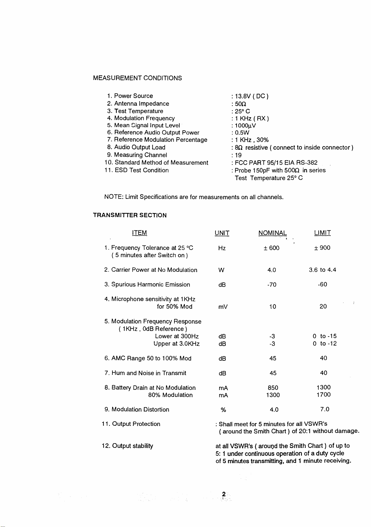
MEASUREMENT CONDITIONS
1. Power Source
2. Antenna Impédance
3. Test Température
. Modulation Frequency
5. Mean Signal Input Level
6. Reference Audio Output Power
7. Reference Modulation Percentage
8. Audio Output Load
9. Measuring Channel
10. Standard Method of Measurement
11. ESD Test Condition
13.8V (DC)
50П
25° C
1 KHz( RX)
1OOOpV
0.5W
1 KHz,30%
8Q résistive ( connect to inside connector )
19
FCC PART 95/15 EIA RS-382
Probe 150pF with 5000 in sériés
Test Température 25° C
NOTE: Limit Spécifications are for measurements on ail channels.
TRANSMITTER SECTION
ITEM UNIT NOMINAL*LIMIT
1. Frequency Tolérance at 25 °C Hz ±600 ± 900
( 5 minutes after Switch on )
2. Carrier Power at No Modulation W.0 3.6 to .
3. Spurious Harmonie Emission dB -70 -60
. Microphone sensitivity at 1KHz
for 50% Mod mV 10 20
5. Modulation Frequency Response
( 1KHz , OdB Reference )
Lower at 300Hz dB -3 0 to -15
Upper at 3.0KHz dB -3 0 to -12
6. AMC Range 50 to 100% Mod dB 5 0
7. Hum and Noise in Transmit dB 5 0
8. Battery Drain at No Modulation mA 850 1300
80% Modulation mA 1300 1700
9. Modulation Distortion %.0 7.0
11. Output Protection : Shall meet for 5 minutes for ail VSWR's
( around the Smith Chart ) of 20:1 without damage.
12. Output stability at ail VSWR's ( arouijd the Smith Chart ) of up to
5:1 under continuous operation of a duty cycle
of 5 minutes transmitting, and 1 minute receiving.
2
RECEIVER SECTION
ITEM UNIT NOMINAL LIMIT
1. Max. Sensitivity pV 0.5 1
2. Sensitivity for 10dB S+N/ pV 0.5 1
3. AGC Figure of Merit 50mV for 10dB ■
Change in Audio Output dB 85 75
. Overall Audio Fidelity at 6dB down ( refer to 1 KHz )
Upper Frequency Hz 2500 2000 min.
Lower Frequency Hz 300 500 max.
5. Adjacent Channel Selectivity dB 55 5
( Two Signal )
6. Maximum Audio Output Power W.0 2.0
7. Hum and Noise Ratio at 1mV dB 0 30
8. Squelch Sensitivity at Threshold pV 0.5 1
9. Squelch Sensitivity atTight pV 1000 250 to 000
10. Image Rejection Ratio ( 900KHz ) dB 70 60
11.1F Rejection Ratio 1st and 2nd dB 70 60
12. 1/2 IF Rejection Ratio dB 70 60
13. Spurious response (22.73 MHz 0CH) dB 50 0
1 . Oscillator Dropout Voltage V 9 11
15. Battery Drain ( at DC Power Jack + 13.8V)
(a) No Signal mA 100 200
(b) Max. Power mA 800 1000
16. Distortion %7
3
2. ALIGNMENT PROCEDURE
1. PLL PORTION
A) EQUIPMENT
B) CONDITION
C) ALIGNMENT
STABILIZED DC POWER SUPPLY
DC VOLTMETER
RF POWER METER
OSCILLOSCOPE
FREQUENCY COUNTER
DUMMY LOAD ( 500 )
SUPPLY VOLTAGE : 13.8V ( DC )
STEP CONDITION
OFTHE
DEVICE
EQUIPMENT
CONNECTION ADJUSTMENT PROCEDURE
1TX 0CH DC Voltmeter
to TP1 L201 Adjust L201 for 1.5V ± 0.1 V as
read on DC Voltmeter.
2RX 0CH Ditto L200 Similarto step 1
3TX/RX
1 - 0 CH Ditto -Check DC voltage of all channels
for within 1, V - 3. V
NOTE 1) Frequency tolérance must meet with spécification.
LOCATION OF ADJUSTMENT ( PLL )
.4
A) CONDITION SUPPLY VOLTAGE :13.8V (DC)
LOAD RESISTANCE : 50 fl
INPUT SIG. FREQ. (AF) :1 kH z
CHANNEL SET :19CH
Set Controls and switches as follows unless otherwise specified.
2. TRANSMITTER PORTION
B) ALIGNMENT
STEP CONDITION
OF THE
DEVICE EQUIPMENT
CONNECTION ADJUSTMENT PROCEDURE
1Input 500mV
19 CH
Connect RF PWR
meter to ANT.
JACK ( J600 )
L102 ( WHT)
L105 ( GRN ) Maximum reading of RF PWR meter.
2No Input
( No Mod. ) Ditto L102 Rotate the core of the L102 clockwise
to read Watts on RF PWR meter.
3 Ditto Ditto -Confirm frequency of all Channels
within spécification.
NOTE 2) DC stopping capacitor is required for MIC signal input linę since
DC current appears on Pin No. 2.
Mic. Jack
J200 777
16V1p(x
4---------О
-----------------------
Оto MIC Signal
LOCATION OF ADJUSTMENT ( TX )
5
3. RECEIVER PORTION
A) CONDITION
SUPPLY VOLTAGE : 13.8V ( DC ) CHANNEL SET : 19 CH
ANT. LOAD IMPEDANCE : 50 П RF SIGNAL FREQ. : 27.185MHz
MOD. SIGNAL : 1 kHz, 30% Mod. RF SIG. OUTPUT : OdB = 0.5pV
STANDARD OUTPUT : 500 mW (2.0V) LOAD IMPEDANCE : 8 П
Set all Controls and switches as follows unless otherwise specified.
SQUELCH : MIN.( FULLY CCW )
B) ALIGNMENT
STEP CONDITION
OF THE
DEVICE
EQUIPMENT
CONNECTION ADJUSTMENT PROCEDURE
119 CH
Volume=Max
( fully CW )
Signal Generator
to J600.
AC Voltmeter to
J201.
L2 to L5
Adjust coils to maximum reading or
the AC Voltmeter.
Keep RF signal level of the sign
gen. to mee.t standard output level
slightly less level during this alignme
STD output at -2dB input.
2Volume=Max
SQ = Max
( fully CW ) Ditto VR1 Set RF Signal ouput level of the sign,
generator to 66dB, then adjust VR1 t
to just “open“ squelch.
LOCATION OF ADJUSTMENT ( RX )
6
3. SEMICONDUCTOR LEAD IDENTIFICATION
DIODES
1SV68 IN4148 IN4003
»
HZ3B2
HZ5B3
HZ601
HZ9B3 С
А
С : Cathode
А : Anode
2SC2001
2SC1675
2SA733
2SC2314
2SC945A
2SC1674
2SC941TM
DTC144 S
1 2 3
2SC3242
2SC2078
В С Е
В : BASE
С : COLLECTOR
Е : EMITTER
1 GND
2 OUT
3 IN
7
. IC INTERNAL DIAGRAMS
SM5125AM
TDA1905 OLTTPUT [
V8 [
BOOTSTRAP [
THRESHOLD [
MUT1NG [
INVERTIN [
SVR [
NON INVERT [
INPUT
" W 16
15П
1 ]
13]
12p
11
юр
9
] GND
GND
GND
GND
GND
] GND
GND
] GND
8
(MODEL)
UT3 8ZP
(SYMBOL)
C001
C002
C003
C00
C005
C007
C008
C009
сою:
5. PARTS LIST
Parts are subject to change without prior notice.
PRO501XL
(PARTS CODE)
GCMB130377Z
GCMT130376Z
GHDL330378Z
GMSC 80 07Z
GNBP330379Z
GNBY330380Z
HBCT 3038 Z
HCSR330381Z
HHDE 30382Z
HHDP 30876Z
HHDZ 30383Z
HHSK 1892 B
HMHG 02919Z
HSDC 31235Z
HSDP 30877Z
KDPT 30385Z
PLBC 821 7Z
PLBS 31081Z
PLBZ 31181Z
RCUN 05 17Z
RCUN 12259Z
RETC33071 Z
SSCW 30050N
UBUD 29900Z
UTUD013 8ZA
UTYY58000ZB
VNYL2323758
VNYL3101500
VNYL3102500
VNYL3203000
WBXC330 2 Z
WCTZ 30 25Z
WSFC330 26Z
WSLV 18706Z
SSCW193008N
SSCW295010N
SSCW3 3006N
SSCW5 0050N
SSCW803006N
SSCW803008N
SSCW80301 N
BCHR81180 Z
BCKM811026Z
BCKQ811030Z
BCKM811026Z
BCAB811006Z
BCKQ811030Z
BCHG81221 Z
BCKM811026Z
BCKQ8.12230Z
BCKQ811030Z
J:* Ł\J-0 .
(DESCRIPTION)
CASE:BOTTOM
CASE:TOP
HOLDER:LED
SCREW'.MOUNTING
BUTTON:PUSH
KN OB
MOUNTING BRACKET
CHASSIS:REAR
HOLDER'.IC
HOLDERPCB
HOLDER :BUTTON
HEATSINK
HANGER :MICROPHONE
SHIELD CASE
SHIELD PLATE
WINDOW
LABEL:WARNING,DC CORD
LABEL:SERIAL NO
INDY 800 LABEL
CUSHION
SPACER
PROTECTION COVER
HEX NUT
INDY 800 CARD
OWNER'S MANUAL
FCC RULES PART 95
VINYL BAG
VINYL BAG
VINYL BAG
VINYL BAG
DISPLAY BOX
SHIPPING CARTON BOX
STYROFOAM PAD
SLEEVE
SCREW:BIND HD +
SCREW:TAPPING ROUND HD +
SCREW:TAPTIGHT BIND HD +
WASHER-.STAR
SCREWP T1GHT BIND HD +
SCREWP TIGHT BIND HD +
CAPACITOR :CER AM IC TS 2.5 S
CAPACITOR:CERAMIC TS 2.5 S
CAPACIT OR:CER AM IC TS 5.0 S
CAPACITOR:CERAMIC TS 2.5 S
C:ELCTTS2.5C+ (D5*11)
CAPACITOR:CERAMIC TS 5.0 S
CAPACITORiCERAMIC TS 2.5 S :
CAPACITOR:CERÄMIC TS 5.0 S
CAPACITOR:CERAMlC TS 5.0 S
ABS .BLACK
ABS .BLACK, SILK
ABS .BLACK
ABS .BLACK
ABS,BLACK
ABS,BLACK
SPCC.1.2T.MFZN3
SECC.1.0T
SECC.1.0T
SPTE.0.5T
SUS30 OR C7701 R.0.2T
C5191R, 0.5T
SPCC.1.0T.NI
SPIE 0.3T
SPTE.0.3T
PC,1.0T,SILK
PAPERPRINT
PAPER
POLYESTER FILM.0.05T
NEOPRENE SP 2T
NEOPRENE SP 6T
COATED BOARD
M5 NI
PAPER
320X370X580X0.07T
100X150X0.1 T
100X250X0.1 T
200X300X0.1 T
**
M3X8 NI D5X10 NI
M3X6 NI
D5NI
D3X6 NI
D3X8 NI
D3X1 NI
18PF 50V J RH TAPI NG
0.001 UF 50V M YD(D)TAPING
0.01 UF 50V ZYF TAPING
0.001 UF 50V M YD(D)TAPING
10UF 50V M TAPE
0.01 UF 50V ZYF TAPING
220PF.50V J SL TAPING
’ 0.001,UĘ 50V M YD(D)TAPING
0.022UF-50V ZYF TAPING
• 0.01ÜF 50V Z YF TAPING -