RCAVICTOR AR-88.LF User manual

..
I
1
1
~.
-,,',
i
) i
!
i-
I '
\ ,
.
~
(,
I
••
J..
l'
i
COMMUNICATIONS,
RECEIVER
.
~
.....
"
..
-,
'.
':.~.
c •
. .'
"~'
..
::\~~
•
~,,,:..;.:.:lI~
.....
--
',-,
MODEL AR-88.LF
"
.•
_.~IN$TRUCTIONS_
"'"
n'U
f"
c t U
red
by
.
.
~
....
:..-.,.
~
.~
';":'-~_r-"'"
"-.:~'-
.
.... .
.'
RCA Victor
'Company,
Limited
M 0 n t
rea
I.
Can
a d a
,
'\
t .
..
:.(
-
,--
",'
",
:~=
PRINTED
IN
CANADA
1137'15·1
-
.
..
.•
_._'-"C.-:'-,.
',:1
~"'.~-~'"
~~~_~,..:.....
-
..
,'
.....
...,..--:;
....
.
:,,:,.
•
_~~,~~,~~,E-.,
..
:~
~.~
,',
..
'
--
<~:-:
'-~~
";:
,:
....
--';
..
".
~
.~,
......
,......
. .
*--
'.'"
. ".,-,' ,.• ::
~
'.
~
..
,.,0.
.f"
.
.....
'" -
..
.'
~
..
~,'
,
.)
• p -
.'
-~
•
".---.-
~
J-
~~,
•
-.
.
•.
>'
•
~
'~
..:
••
":~.J_,,.,
.•.
"',".-;';,-.
c;.·
-......-
".·c
.-
:,-.;:.:~"",
:,~~
..
:
..
~.,...
:-~
.•
-~~
..
,::",,;.--. :
""
';
.:-'
.
..

••
•
Figure
]
.~General
Purpose
Communication
Receit1er-Front
Vietc.
•
'-,"-"
)
..
.Figure
2.-GcTlcral
Purpose
Communications
Recciver-Loud.speaker.
[2J
\
-;
,
....

. .,..,-'
GENERAL
PURPOSE
COMMUNICATIONS
RECEIVER
INSTRUCTIONS
1. GENERAL
1.1 Thi!t
n~cei\."cr
has be(;fl designed for general pur-
pOSt!
cummunication.
It
is.
designed
to
withstanJ
scvert! climatic
and
line \'oltage variations.'
without
appreciable:
impairment
in performanc-:..
1.2
The
following> features
hayc
been
incorpurateJ
into
the
design
of
this
unit.
(a)
Mechanical
Band
Spread, }"ith Single
Con·
trol for ease
of
tuning
a previousl)' logged
station.
(b)
Automatic
Noise Limiter
which
automa-
tically limits
interference
to a percentage
of
modulation. .
(c)
Noise
Limiter
Switch for switching Noise
.
Limiter
on
or
off.
(d)
Continuously
variable
High
Frcquenc)'
Tone
Control.
(c)
Panel
Antenna.
Trimmer
ft.)r
circuit align·
~t
ment.
(f)
Variable
selectivit)"
with
expansion
of
the
normal selectivity characteristic for stand-
br,
and
a crystal filter for
ultra
sharp
selec·
tivity
when
required.
The
crystal filter circuit
is
adjusted
at
the
factory to give selectivity
characteristics as
shown
in
Figure 12.
(g)
Temperature
compensated oscillator circuits
on
all bands.
(h)
Regulation
of
the
anode voltage
of
the
oscillator,
giving
good
oscillator stability
through
normal
variations in line voltage.
(i)
Four·ganged
Condenser
gi"ing
high image
ratio,
and
very
low oscillator radiation
on
all. bands.
(j)
Special screening
d"'ices
have
been
built
around
the
gang
condenser,
the
master aScii,
iatur'section, anti the r.t. amplifier secti
..
}n
ir.
orJer
to
minimi:c
.9::..:i!lawr radiatiun
u:'i
0:1.11
bands,
(k)
Tuning
lock
for
sance
under
extreme::
con-
ditions
o'f
\ribration.
1.3
Frequency
Range:-
Band
1
73
to :!05
KC
Band
2 195
to
550
KC
Band
3 1480
to
4400
KC
Band
4
4250
to 12150
KC
Band
5 11900
to
19500
KC
Band
6 19000
to
30500
KC
1.4
Sensitivity:-Better
than
15
microvolts
for
20
dh
signal to noise ratio,
for
MC\V'
(
..
\·1)
reception
and
better
than
5 microvolts for
CW
(A·
1) reception (see
tahle
No.
1).
1.5
Radiation:-Lcss
than
40 mkro-mkrowat::s.
of
power
radiated,
as
dissipated in resistance .:on·
neeted frum
Antenna
input
terminal
to
grouno.
Value
of
resistance is sueh as to cause m:'ximum
power
to
he
radiated
(scc Section l
helow).
1.6
Output
Power:-(Maximum
undistorted)-2
.
.5
Watts
when
loudspeaker
used.
When
lo\.\.-
im-
pedance
headphones
are used,
maximum
output
fed
to
the
phones
is
lOO
milliwatts
approximate'
ly.
1.7
Pow...
Supply
Requirements:
-
11
5
or
1,0
.
"bIts,
15/60
cycle, 100
Watts
or
6
volt.
D.C.,
11
amps
when
external
power
supply
MI·22213
is
used.
(Note-external
power
supply
MI-:!:!:!15
is
only
supplied
wh'en specially
ordered.)
1.8
Output
Load:-
-This
receiver
has
pro\'ision in
the
output
circuit
to
take loads
of
'2.5
ohm:s. :!o
ohms,
and
also
low
impedance
headphones.
1.9
Mechanical
Specifications:-Overall
Dime~-ioru
-19t
inches
wide
x
11
inches
high
x
19!-
inohe3
deep.
Weight
--·100
Pounds
(unpacked).
2.
TECHNICAL DETAILS
2.1
Circuit
Details
and
Features:-
The
schematic
diagram
of
this
receiver
is
shown
in
Figure
11.
It
consists
of
two
stages
of
R.F. amplification.
first detector, first
heterodyne
oscillator;
three
of
LP. amplification, second
detector
and
A.V.C.,
noise limiter, second.
heterodyne
oscil-
lator; A.F. amplifier stage,
output
power
stage,
and
power
supply
system.
2.2
Input
Coupling:-
The
antenna
coupling system
is de:;igned to
provide
optimum
coupling from
a .200
ohm
trans,?ission line,
but
equivalent per-
formance is realized
with
a
straight
line
antenna
·'It,
\:l
,
.-~
'.
[4]
(see Section
4.4)
with
a
conventional
lead·in
v.rire.
The
first
tuned
circuit is provided 't\dth a
trimmer
condenser
adjustable
from
the
front
panel.
This
insures
the
proper
tuning
of
this
circuit
with
any
antenna
system.
For
all
bands,
conventional
antenna
and
ground
connections
may
also
be
used.
The
antenna
.terminal
board
is
pro,~ded
with
three
terminals (see Figures 3
and
7),
rn'o
of
which
may
be
joined
together
with
a link.
\Vhcn
a
sin~le
",';rc
antenna
is used,
the
link
should
be
closed
and
the
antenna
connected
to
"A".
If
a
ground
is
used,
it
should be
connected
to
·~G"".
!
•
•
•
..
,
,
(
..
"
..
,
·
-.'

•
•
-.
.-..ci
..
If
a transmission line
or
balanced
input
is used,
the
link should
re
opcned
and
the
line con-
Ih;..:t..::J to t":[I111nal ".i\"
and
the
c~lller
tcrmilld.l.
Protectioll
against
damage
Ju('
tl)
high
yoltagcs
acrOS$
the
antenna.
coil
primarics
is
provided by
a gas gap
protector
(Type
991
Valve).
This
protector
will
brc3.k
down
with
an
applied
potential
of
approximately
.50
Volts
R.M.S.
1.3
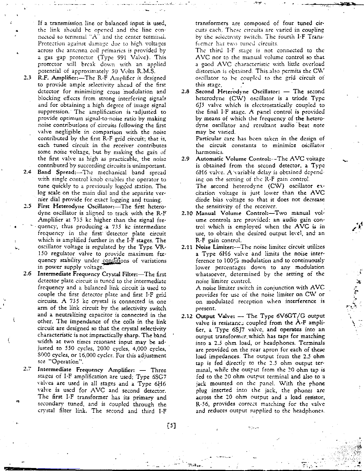
R.F.
Amplifier:-
The
R·F
Amplifier
is
designed
to
provide
ample selectivity
ahead
of
the
tirst
detector
for
minimizing cross
modulation
and
blocking effects from
strong
interfering
signals:
and
for
obtaining
a
high
degree
of
image
signal
suppression.'
The
amplification
is
-adjusted
to
provide
optimum
signal-to-noise
ratio
by
making
noise
contributions
of
circuits following
the
first
valve negligible
in
comparison
with
the
noise
contributed
by
the
first R-F arid
cir~uitj
that
is,
each
tuned
circuit
in
the
r~ceiver
contribut~s
some noise
"(:'oltage,
but
by
making
the
gain
of
the
first valve as high as practicable,
the
noise
contributed
by
succeeding circuits
is
unimportant.
2.4
Band
Spread:-
Tho
mechanical
band
spread
with
single control knob enables
the
operator
to
tune
quickly
to
a previously
Jog~£ed
station.
The
log scale
on
the
main dial and
the
separate
ver~
nier
dial
provide
for
exact
logging
and
tunina'.
1.
.5
First
Heterodyne
Oscillator:-
The
first
he:te~o'
dyne
oscillator
is
alig1"!eu
to track
with
the
R
..
F
Amplifier
at
735 kc higher.
than
the
signal fre·
.
quenq",
thus
producing
-a 735 kc
intermediate
frequency
in
the
first'
detector
plate
circuit
which
is amplified
further
in
the
I·F
stages.
The
oscillator voltage is regulated by
the
Type
VR·
150
regulator
valve to
provide
maximum
ft.e-
quency
stability
under
con.dit~ons
of
variations
in
power
supply
voltage.'
2.6
Intermediate
Frequency
Crystal
Filter:-
The
first
detector
plate
~ircuit
is
tuned
to
the
intermediate
frequency
and
a balanced
link
circuit
is used
to
couple
the
first
detector
pla.te and first I·F grid
circuits. A
735
kc crystal is
connected
in
onc
arm
of
the
link circuit
by
the
selectivity
s'W-itch
and
a
neutralizing
capacitor is
connected
in
the
other.
The
impendance
of
the
coils
in
the
link
drcuit
are
designed
so
that
the
crystal selectivity
characteristic is
not
impractically sharp_
The
b:tnd
width
at
two
times
resonant
input
may
be
ad-
Justed
to
550 cycles, 2000 cycles, 4,000 cycles,
SOOO
cycles,
or
16,000 cycle,.
For
this adJustment
sc~
"Operation".
2.7
Intermediate
Frequency
Amplifier: -
Three
stages
of
I·F
amplification are used;
Type
65G7
yah-es
are
used in all stages
and
a
Type
6l:i6
nh"e
is
used
for
A
VC
and
second detector.
The
first I-F
transformer
has its
primary
and
secondary
tuned.
and
is
coupled
through
the
crystal filter link.
The
second and
third
I·F
[5]
'.-.~.:
.'-'.':'p"qfi'---
transformers
are
composed
of
four
tuned
cir-
cuit~
each. Thc:,c circuits arc varied in coupling
by
th..:
s,,;k,,:u\"l[Y
swit..:h.
The
fourth
I-F Trans·
furma
hit!:
t\.\"()
tuncJ
circuits.
Th~
third
I-F
stage
is.
not
connected
to
the
A
VC
nor
to
the
manual
volume
control
50
that
a good A
VC
characteristic
\\·ith little overload
distortiun
is
obtained.
This._also permits tht:
C\V
o~cillator
to
he
courkJ
to
the
grid circuit
of
this stage,
2.8
Second
Heterodyne
Oscillator:
-
The
se.:ond
hcterodyno
(CW)
os<illator
is
a
triode
Type
GJ5
valve
which
is electrostatically coupled
to
the
final.
I-F
stage.
.A
panel control is pro\-ided
by
means
of
which
the
frequency
of
the
hetero-
dyne
oscillator
and
resultant
audio·
beat
note
may
be
·varied.
Particular
care
has
been
taken in
the
design
of
the
circuit
constants
to
minimi:e
oscillator
harmonics.
2.9
Automatic
Volume
Control:-·-
The
AVC
voltage
is
obtained
from
the
second detector, a
Type
6H6
....
ah-~.
l\
'yariable delay
is
obtained
dcrentl·
ing
on
the
setting
of
the
R,F gain control.
The
second
heterodyne
(CW)
oscillator
ex'
citation
,.-oltage is
just
lower
than
the
A
VC
diode bias
....
oltage
so
that
it does
not
decrease
thl! sensiti\"ity
of
the
receiver.
2.10
Manual
Volume
Control:-Two
manual
vol~
ume controls
arc
pro
....
ided:
an
audio gain
con'
trol
which
is
emplored
when
the
AVe
is
in
use,
to
obtain
the
desired
output
le\-ei, and'
an
R·F
gain control.
2.11
Noise
Limiter:--
The
noise
limiur
cin.:uit utili:.es
a
Type
6H6
valve
and
limits
the
noise inter-
ference
to
100fo
modulation
and
to continuously
lower
percentages
dO\"'n
to
any modulation
whatsoever,
determined
by
the
setting
of
the
noise limiter cuntrol.
A noise limiter
switch
in
conjunction
~'ith
A
VC
provides
for
use
or
the
noise limiter
on
C\V
or
on
modulated
reception
when
interference
is
present.
2.12
Output
Valve:
-
The
Type
6V6GT(G
output
valve is resistanc.:;
coupled
from
the
A·F
ampli~
fier, a
Type
65]7
vah'c,
and
operates
into
an
output
transformer.
which has
tap!
for
mat~hing
into
a 2.5
ohm
load,
or
headphones.
Terminals
are provid.:d
on
the
rear
apron
for
each
of
thc...~
load impedances.
The
output
from
the
2.5
ohm
tap is fed directly to
the
~.5
ohm
output
ter-
minal, while
the
outrut
from
the
~o
ohm
tap is
fed
to
the
~O
ohm
outpUt
terminal
and
alSt)
to
a
jack
mounted
on
the
panel.
With
the
rhone
plug
inserted
into
the
jack,
the
phones
arC
across
the
20
ohm
output
and
a load resistor.
R-56,
pro\;des
corre..:t
matching
for
the
valve
and reduces
output
5upplied
to
the
headphonc:;.
:-.
-,:: . "
"
.'
.'.
r
\

...
':.
-----._.
-w
_'
..
---
-.
.•
2.13
Power
Pack:--The
power
pa..:k
mounted
on
the
r('~.:i\·I.~r
~h;\~~i5
~on5i5t5
of
a
power
rran:;:funner,
r..:~::h..:r
YJ,h-·.:
Typ..:
~Y:l~T,
(; J.EJ
tiI:,;,;
.•
\
tVb~l.:
~wit,;h
i~
I'f()YidcJ
on
rh.: rc.lr
arror.
f"r
chaI1>!"
ing
the
power
transformer
yoltagc
rar
to citht:'r
115
or
2~O
Volts.
The
instrument
may
also
h~
operated
from
6V.
"A"
and
c50 to
:00
V.
"B"
battaies.
(See
Section
1-4).
2.14
Vibrator
Power
Unit:-
The
M.r.-22'216
Vibrator
Pov.:er
Unit
is
designed
for
us~
with
this
Re-
ceiver
to
supply
the:
DC
yo!tage necessary
from
6 \'olt
DC
battery.
It
is a
separate
ass<mbly
and
is
tined
with
a
plug
to
attach
it
to
the
receiver
•
by
means
of
Socket
J-l
on
the
rear
apTtJn.
(Note.
---ThIS
Vihrator
Powa
Unit
is
only
supplied
\\;--...
;1
sp":":ld.liy
unl..:reJ.)
It
(,~)n5i::t::
of
non·syn..:hrnnou5 'Vir-raroT used
i~
LonJunction
with
a
step-up
tra.nsfonner. Rc.:tifi-
cation
is
obtaincJ
by
the
use
of
;1
typ~
OZ.;.A
\'alvc:
(SI?C
Section 7
below.)
2.15
Shielding:-Interstagc
shielding IS
pro\-idcd
to
insure sta
..
biliry
under
all
operating
condition~
and
to minimi::.e
oscillator
radiation.
Complet~
external
shielding
pre\'cnts
coupling
to
a.ny
par·
tion
of
the
circuit except·
through
the
antenna
circuit.
3.
PERFORMANCE
3.1
The
performance
data
belo":'
and
the
data
for
the
various
curves,
(Figuus
12, 13, 14)
arc
approximate
values
taken
on
a sample receiver.
Variations
in
these
values
a.re
to be
expected
because:
of
practical
manufacturing
to1erances.
The
data
were
taken
with
an
artificial
antenna
of
700 mmf. capacity
for
hand
I
and
c
and
"00
ohms resistance for
bands:';
to
6 inclusi"·e.
The
output
was
measured
across a resistan_ce
of
2.5
rhms
connected
in
place
of
the
speaker
"'oice coil.
The
selectivity switch
was
placed
in
position
:!
unless
otherwise
stated.
Figures
are
for
MC\\"
(A.-:?) rc('epti-on, unless
otherv.;se
stated.
'-
3.2
Performance
Data:-Approximate
values
only-
Taken
on
Sample
Recci\'er.
(See
Ta~k
I.)
TABLE No. I
Band
1
2
"
:J
4
5
6
f Frequency
I in
Ko.
I
i 140
I 195
;
I 205
I 375
I 500
I
I
,
I
1,600 I
i 3,000
! 4.250
4,+00 I
; 7,500
I
I 11.900
! 12,100 I
i 15,500
19.000
19,500
~'7.500
30.000
Input
in microvoits
for
10
db
s. to n.
C\\'?(A·l)
re<:eptton
..
3.1
2.8
1.8
2.6
3.7
2.6
1.9
1.8
3.7
2.0
1.8
1.7
2.9
-
2.'
1 •
_.,
3.0
".8
I
.,
,
I
I
I
I
I
i
i
;
;
,
!
!
I
I
Inpl.:t in micro\'oits
fo:
10
db
s.
to
n.
1"0
_.
12.5
10.5
6.0
8.0
9.8
8.0
6.5
0.0
9.5
'1.9
. 7.0
7.0
8.2
7.0
7.5
7.9
7.7
,
,
,
!
I
I
I
I
I
,
:
i
I
I
I
I
Image
Ratio
I . I •R.adiatlon
.
I.F.
Rejection Ratio fron:.
Qs.cillilor
I in micro·.a::icro
....
.ltt!
t
th
1
000000
grea er
an
t
th
1
000000
1
lC3S
than
05
grea er
an
..
I
..
..
~
I .05
..
1,000,000 .
..
" .05
..
1,000,000
..
..
.05
..
1,000,000
..
..
.05
1,000.000 I 37,000
..
..
.05
,
1.000.000
greater
than
1,000,0001 .05
.1
100,000 ,
,.
..
~
.03
,
c5,OOO
..
..
..
.05
600.000
..
..
..
.05
11.000 ,
..
..
..
.05
6,000 !
..
.. ..
.05
,
15,000 ,
..
..
..
.03
5,000 ,
..
I
.09
.
>,100 .05
4.000 .05
600 .135
375 .300
• R"d:.l.leJ
J."O"'er
musured
IS
that
JJSUP3t",..l
In
a
re5uto~
c.1nnecltU from Am::::n:u
f'USI
t
...
,.:wun..l.
V.due
of
reSJstur
IS
thJ.t
"'hKn
ren:H.
::::.
="XI:.".";;'
~ll"'-er
bc::'I":
.r~di.ued.
[6]
--
•
•
(
(
•
•
(
~

•
•
\
'.
,
....
3.3 . Oscillator
Stability:-
(a)
Oscillator frequency
",,,1.
within
O,OOI],c
for
line
\"oltJ.gc YJ.riatinl1
rf
:::
5~(-.
(b)
Oscillator frequency stable
within
0.000%
for tempcratur.:: chang\,' nf 1
::c.
(c)
Oscillator
frequency
stabl~
within
0,1)01:"(
for
total
variatiun
of
both
.the audio
and
R.F. gain controls.
(d)
Resetting
of
ranc:c switch from either
din~c'
tion
does
not
\:ary
the
frt:quency
of
the
oscillator
on
any
hand
more
than
1 kc.
3.4 Dial
Resetability-bttter
than
2 kc.
when
the
dial
is
reset from
either
direction,
at
any
frequency.
.3.,)
Dial
Calihrati"n:-C;di~ration
of
tht: dial is
accu'
rate
to
within
O.5
c
(-.
3.6 A
VC
Chara('tcris~ics:--Thc
A
VC
..
-ir,,::ulc
holds
th~
auJio
output
k\·e\
to
12
db
wh("n thi:
MeW
(A·2)
input
IS varied between 10
and
100,000
·microvoir.::
at
any
fr~'-lucncy,
with a.ny
modula-
tion percentage frum
11)
to
90,
and
\\;th
any
modulation
fx:.~qu(;ncy
from
~00
to
400')
cy..::les.
(Sce Figure
H.)
:--~
.,
4.
INSTALLATION
4.1
Power
Supply:-The
power
,upply
circuit
is
integral
with
the
receiver. Determine line volt-
age
and
frequency and check
with
the
rating
of
the
receiver.
The
power
transformer
primary
may
be
connected
for
either
113
or
230 volts
23/60
cycle
by
means
of
the
toggle switch
on
the
rear
apron.
This
toggle
~
switch is protected
by
a
protector
plate.
To
alter
the
conne.:tion
of
the
primary, remove
the
protector
plate,
throw
the
switch,
and
replace
the
prot..:ctor
plau,
'\vith
the
reverse face out.
4.2
For
Battery
Or
Other
Supply
O,Peration:-For
connections see S'Chematic Diagram Figure 1t.
It
is only necessary
to
remove
the
plug
from
the
socket
on
the
.rear
of
the
recei
....
er,
and
connect
the
batteries
to
the
proper
terminals as indi-
cated
by
the
schematic diagram. A
battery
cable
terminating
in
9-n
octal male plug
is
neces'
sary
for
this
purpose.
If
the
Vibrator
Power
Unit
MI·22216
is
used,
remO\'e
the
plug from
the
socket
on
the
rear
of
the
receiver.
and
plug
in
the
cable from
the
Vi·
brator.
Power
Unit.
Connect
the
6 volts D.C.
input
to
the
power
unit
with
heavy, low resist-
ance leads. See Section 7. for
more
detailed
information
concerning
the
Po\ver Unit.
4.3
~ah'es:-Inspect
the
chassi::
before
applying
LIN£
VOl.'Au£
AO./VSTM£NT
SWITCh'
o
POVE.~
OMS
CO,ep
TO
,el'lNSl'1lTTCe
.eE;l..AY
roe
8ATT£e
y
opeRATION
eTC.
R£MOV£
PLV<U
CO/'fNE.fT
8I1TT£,eV
TO
SOCK€T(O/-I
.
power
to
see
that
all
val~'es
are firmly seated in
their
respecth-e sockets.
._
4.4
Antenna:-
The
input
impedance
at
the
an-teMa
terminals
is
designed to
match
a 100 to
~oo
qhm
transmission line
or
a
straight
wire capacity,
type
antenna.
For
general use
it
is recommended
that
a
straight
wire
antenna
between 25 and
50
feet
long
be
used
for
bands 3 to 6 inclusive,
and
a.
........
wire
of
200 feet
or
more
for
bands
1 and 2.
4.5
Spe-aker:-
Terminals
for connection
of
a
loud·
sp..:aker
arc
inJkat.:J
in
Figur~3
?-
and 7.
The
output
transformer
is
designed to match a
p.m.
dynamic
speaker
having
2.5 ohms impedance.
4.6
Headphones:-A
jack
is
pro\;ded
on
the
left
of
the
front
panel
for
plugging in a
pair
of
head·
phones.
If
additional phones are required.
the)'
ma),
be
conn.:..:tcd to
the
20
ohm
output
ter-
minals on
the
rear
apron
of
the
receiver.
Phones
ha'\"ing
an
impedance in
the:
range
of
11::
..
)
to
600
ohms
should
be
used.
4.7
Mounting:-
The
instrument
may be placed on
a
table
or
mounted
on
Cl-
rack.
For
rack
mount-
ing
loosen
the
panel mounting screws·
and
re-
mo'\'e
the
front
panel
and chassis compiete
from
the
cabinet.
Then
mount
on rack by
r:lean~
of
the
slots at
the
sides
of
the
panel.
ANTCNNI'I
COIL
INOt/CTANe£
.€CA
-
/lOO!}7
AO./VSTM£NTS
FOJ?
I'Il-L
IJANpS
61/5
U"lP
PROT£CTO.e
WAVC
T.eAP
'"
T8.
(
'\
ANT-GNP
TC.eH.
8D.
Figure
3.-General
Purpose
Communicatiuns
Rcccieer-Rear
Apron
[7]
EZJC)
:.
..
..

'.
5,
OPERATIO~
5.1
Bci,)rc
attcmring
to
orerate
the
rccei\"a.
the
information contained in this section should be
thoroughly
understood
by
the
operator.
Tn<!
symhols
on
panel u5cd
to
desIgnate
the
various
controls
as
shu\vn in Figure
1,
should be learned
with respect
to
function, as described
h~r~in.
5.2 The-
Antenna
T
rimmer:-
The
center
knob
on
the left is
the
Antenna. Trimmer. Before tuning
on
any
frequenc)' range, it should
be
adjusted
for maximum performance on
the
band.
This
control
may
be
adjusted
-by
tuning
for
maximum
background
noise.
Occasionally
it
is desired
to
test
a.
signal
that
seems
out
of
place, to see
whether
or
not
it
is
a
fundamental signal
or
an
..image
....
Wlfen
doing
this, if
the
maximum signal
point
coincides v·:ith
the
point
of
maximum
background
noise,
the
signal is a fundamental.
If
the
control
doe,
not
affect
the
signal strength,
or
if
it
is
'a maximum
at some
other
point, it
is
an
"image",
5.3
The
Main
Tuning
Dial
is
on
the
left and con-
sists
of
Cl
disc
with
SC\'en
scales, one for
eac~
of
the
six
bands
and
a log scale.
The
twe
lo\\' fre·
quenc)'
bands
are calibrated in kilocycles
and
the
other
four
bands in megacycles.
5.4
The
Vernier
Tuning
Dial is
in
the
center
and
has a scale
with
arbitrary
calibrations
for
exact
tuning
and
log records
of
particular
communica-
tion stations.
It
is used
in'
COn
junction
with
the
log scale on
the
main
tuning
dial to give addi·
tional figures
for
logging.
5.5 Power-
Transmit-Receiver
Switch:
-
This
is
a
four-positiop switch:
Starting
from fully coun·
ten:lockwise these positions are:
1.
Power
off.
~
Transmit
position
which
gives energi:.ecl
tube
filaments,.
open
plate
circuits, and
shorted
terminals
(for
transmitter
relay)
on
the
speaker
terminal
board
on
the
back
of
the
chassis. (3.
fi
4.
on
T.B.·Z.).
Connect
rday
to
these two terminals for transmitter
operation. (See Figure 3.)
.
'.
Normal
reception.
4.
CW
reception -Beat
frequency
oscillator
switched
on.
5.6 Selectivity
Switch:
-
This
is
a five-posinon
switch and
the
band
widths
and
control
of
selectivity are illustrated in
the
curves
of
Fi:;urc
11.
The
five positions are:
1.
I·F
band
width
for
High
Fidelity, modu·
lated reception, -
for
"Stand·by"
use.
o
I.F
band
width
for
normal
modul"teJ
reception.
>.
Crystal
Filter in -for
CW
telegraph
or
sharp
modulated signal reception.
'
..
[8}
Cryst..d Filter
in
- -
for
!-harf'Lr
CV".,
tele-
graph
reception.
...
Crystal
Filta
in -for snarr\:.5t
C\V
tele·
graph
reception.
5.7 Noise
Limiter-A
VC
Switch:-
This
is
a four·
position switch
and
starti~g
from
the
fullr
counterclockwise- position thc.x: are:
1.
A
VC
and
NL
out
_.
Manual
gain only -
for
CW
-
n'o
interference.
o
NL
on, A
VC
out
-
Manual
gain -for
CW
\vith interference.
,.
Nt;. and A
VC
on
-for
Modulated
Recep'
tion
with
interference.
4.
A
VC
on,
NL
out
--
for
ModulateJ
Re<ep·
ticn
-no interference.
S.B
RaF
Gain
Control:-
This
continuously variable
sensitivity control is
for
use.in conjunction
with
the
audio
gain
(Volume)
control for all manual
gain operation.
With
A
VC
on, it
should
as a
rull!
be
set to its fully clockwise position
or
may
ht::
turned
to
eliminate interfercn;:c-.
For
re..:ep-
tio!1
of
strong
CW
signCils,
it
mu::
he
retarded
somewhat.
5.9 Noise Limiter
Control:-
This
control sets
the
instrument
for
operation
at
the
required per-
centage
~'alue
of
Noise
Limitation.
The
fully
clockwise position limits
the
noise
interference
to
1007c modulation.
As
the
knob
is
turned
counterclockwise,
the
noise interference is
lim~
ited to continuously lower percentages
of
modu#
lation so
that
in
the
fully counterdock\.
....
-ise
posi#
tion
the
Noise Limiter
is
operati\.·c
on
ani'
modulation \vhatsoever. Normally.
the
fully
clockwise position will be used,
rut
under
ex"
treme conditions
of
interference
a t-alance point
should
be
found
for
maximum inte!lig:ibilitv
of
signal
with
best modulation
and
lel~t
~oise.
~
5.10
Tone
Control:-This
is a continuously variable
control for reducing
HF
response.
In
the
fully
clo.:kwise position
the
fulI
tonc
is
obtained
and
as
turned
counterdoch,-ise.
high tones arl!
lessened. Set
it
to
suit
the
particular tona.l con·
ditions
for
the
signal
being
received.
5.11 Beat Frequency Oscillator
Control:-
This
con'
trol
is
normally used for
C\V
code signals.
It
should
be
adjusted
to
give
the
desired audio
pitch
after
the signal has heen accurately tuned.
5.12
Tuning:-For
functions
of
controls sce
the
foregoing paragraphs.
1.
Turn
receh-er
on
and
set
the
Powcr#
Transmit·Receive
Switch for
the
requireJ
type
of
operation.
1.
Set
Range
Switch
for
band
required.
3.
Set
Antenna
Trimmer
for
maximum back-
ground
noise.
"
•
•
-
•

•
..
(
'.
...
~ .
_
.....
_-
....
_-
.....
_-
4.
Set Selectivity Switch
for
the
required
operating
conditions
-Sec
Selectivity
Cun:\:s
-
Figure
1:::.
5.
Set
Noise
Limiter-AVC
S\yitch for
the
required
operating
conJitions.
6.
Set
R·F
Gain
Control
fully clockwise.
7.
Set
Audio
Gain
Control
about
halfway.
8.
Tune
in
the
station.
9. Reset
Audio
Gain
Control
to give dcsirc:J
volume.
10. Reset Selectivity
and
Sensitivity
(R·F
Gain)
Controls and
Noise
Limitcr
Control
in accordance
with requirements
due
to in-
terference, station transmission,
and
other
.-
......
:..
canditions. •
11.
Set
Tone
Control
for
preferred
tone.
12.
On
CW
(A-I)
operation set
Power·Trans·
mit-Receive Switch to ·'Rec.
CW"
(position
4)
and
set
BFO
Control
to
give desired
pitch.
When
a
strong
CW
signal
is
being
received,
it
is
necessary
to
retard
the
R.F.
Gain
Control
to
reduce
the
volume.
, :
.....
-.:...:.---
..
-.~
..
-
...
13.
If
the
re":CIya
is
5uhJc(t
tt..) nt--r.lth'J'i.
ch..:
tuning
may
be locked
by
turning
c1od,wi~
tht.:
knurled screw directly
heneath
the
tun
l
ing
knob.
Turning
the
screw moderatel}'
tight
will lock
the
tuning
.
S.13 Diversity
Reception:
-Provision
is
made
to
operate
two'
or
three
of
these receivers
together
for "diversity" reception
..
For
this
typ~
of
r-ecep-
tion
the
A.V.C. circuits
of
the
receivers are tied
together.
The
receivers are
operat~d
on
separa(l"!
antennas,
and
the
receiver receiving
the
strongc.5t
signal,
thus
generating
the
greatest
A.V.C.
volt-
age. dominates
the
other
receivers.
If
the
separ
l
ate
antennas
are
f~es!.
.~.o
~t_he
.incoming signal
at
different angles,
the
good reception \virh mini·
mum fading results.
Refer
to
Figure
3:
Connect
togt::ther
the
ter-
minals, marked '"Diversity"
of
the
receh·ers.
and
equip eaeh receiver
with
a separate
antenna.
Tune
each receiver
to
the
same station
as
ex-
plained in Section 5.12 above.
6.
l\IAINTE.NAc~CE
6.1
This
receiver sh'ould maintain its correct fac-
tory
adjustments
over
a reasonably long period
of
time. Causes
of
trouble
and
the
probable
.sequence
of
their development. are outlined in
the
follOwing paragraphs:
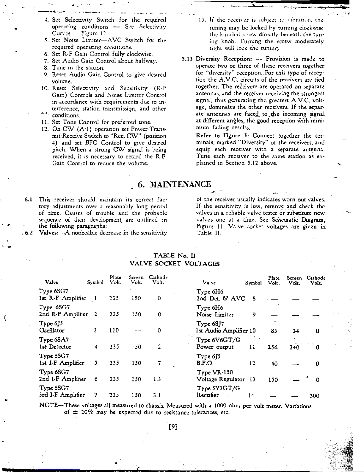
. 6.2
Valves:-A
noticeable decrease
in
the
sensitivity
TABLE
No.
11
of
the
receiver usually indicates
worn
out
valves.
If
the
sensitivity is low, remove
and
check
the
valves in a reliable valve tester or' substitute
new
\'alves one
at
a time. See Schematic' Diagram,
Figure
11.
Valve
socket voltage.s are
gi\Oen
in
Table
11.
V
AL
VE
SOCKET
VOLT
AGES
Plate Screen Cathode Plate
Scre-en
Cathode
Valve Symbol Volt. Volt. Volt. Valve. Symbol Volt. Volt.
VoIL
Type
6SG7
Type
6H6
1st R-F Amplifier
0'-
-"
150 0
2nd
Det. <;
AVC.
S
Type
6SC7
Type6H6
2nd
R-F Amplifier 2 235 150 0
Noise
Limiter 9
Type
6J5
Type
6SJ7
Oscillator 3 110 0 1st
Audio
Amplifier
10
83
34
0
Type6SA7·
Type
6V6GT/G
1
st
Detector
4 235 50 2
Power
output
11
256
240 0
Type
6SG7
Type
6J5
1st I-F
~plifier
5 235 150 7 B.F.O.
12
40 0
Type6SG7
Type
VR-150
2nd
I·F
Amplifier 6 235 150 1.3 Voltage
Regulator
13
150 0
Type
6SG7
Type
5Y3GT/G
3rd
I-F Amplifier 7 235 150
3.1
Rectifier 14 300
NOTE-These
voltages all measured to chassis.
Measured
with
a 1000
ohm
per
volt meter. Variations
of
==
20%
may
be
expected due to resistance tolerances, etc.
[9]
•
..
kill'.
a.
..
_SJ;;"A4
3.
ilsr.
£
-:
•...

6.3
Range
Switch:-A
switch may operate defec·
tively
on
certain positions
after
long periods
of
inct',,:ratifln.
U5U;J.1!y
rotating
the
~wjt..:h
hack
and
forth several times will clean
the
contacts
and
operation will h:.:omc normai.
A
bad
range-switch
contact
is likely to cause a
change
in
the
sensitivity
of
the
receiver,
or
the
frequency
of
a received· signal, as
the
switch is
moved
back
and
forth
.::lightly
in
a
certain
fre-
quenc)'
hand
position. A
further
check
is
to
turn
the
5v.ritch off
and
on
at.
onc
particular
fre-
quency
band
several times
and
note
the
apparent
sensitivity
of
the
receiver
each
time
the
switch
comes into position.
The
sensitivity should be
the
same each time
and
may be aclequaely judged
for
this
test
by
listening
to
the
receiver back-
ground
noise.
6.4 Circuit
Alignment:
WARNING:-The
Circuit
Ali9nment
of
this
receiver
has
been'
done
very
carefully
at
the
factory,
and
re-
ali9nment
should
not
be
attempted
unless
it
has
been definitely
ascer-
tained
that
the
Circuits
are
out
of
ali9nment.
It
should be'
attempted
only
by
skilled
personnel.
It
must
be
performed
in
a
test
laboratory
where
proper
test
equipment
is
available.
All
adjustments
must
be
done
very
carefully
and
the
exact
procedure
as
outlined
below
must
b.
followed.
6"';·1
Alignment
Tools:-Spe:cid.!
tooL~
fa:
align'
ment
of
RJF
and
I·F
circuit5
are
prm:ided.
The)·
are
mounted
in
fuse clips on
either
side
of
the
gang condenser coyer, and
are
a\'aila~lc
after
removing the large
R,P
unit
CQ\'Cr.
Tbe
shorter
onc
of
the
two
is
for
adjustment
of
all
R·F
and
I·F
coils.
and
the
longer
one
is
for adjustment of
the
plunger
type trimmers.
One
end
of
this
tool is for
turning
the
lock
nut
on
the
-trimmers
and
the
other
end
has a hook for
engaging in
the
hole
in
the
end
of
the
plungers.
After
adjustment,
the
lock
nut
should be
sectreIy'
tightened
..
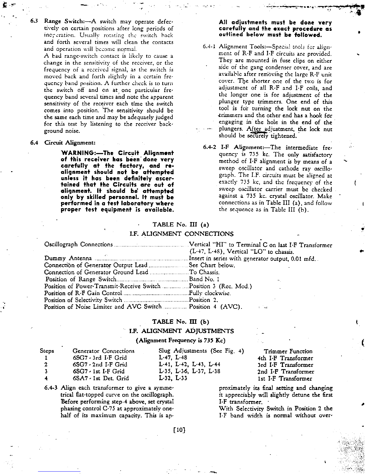
6.4·2
I·F
Alignment:-
The
intermediate
fre·
quenc), is 735 kc.
The
only satisfactory
method
of
I·F
alignment
is
by
means
of
a
sweep oscillator and cathode ray oscillo·
graph.
The
I.F. cir:uits must be ali£ned
at
exactl),
7,5
kc, and
the
frequency-of
the
sweep
os...-il1ator
carrier must
be
checked
against a 735 kc. crystal oscillator.
Make
connections as in
Table
III
(a),
and follow
the sequence as in
Table
III
(b).
TABLE
No. m
(a)
I.F. ALIGNMEI'<'T
CONNECTIONS
Oscillograph Connections .Vertical
"HI"
to
Terminal
C
on
last
I·F
Transformer
(L'47, L-48), Vertical
"LO"
to chassis.
Dummy
Antenna
.............
..
...
.Insert
in
series
with
g~nerator
output, 0.01 mfd.
Connection
of
Generator
Output
Lead
...
Connection
of
Generator
Ground
Lead
..
Position
of
Range
Switch .......................
See
Chart
below.
..
..............
.To
Chassis.
.
...
Band
No.
I
Position
of
Power-Transmit-Receive Switch ... Position 3 (Rec.
Mod.)
Position
of
R-F
Gain
ControL
...................
..
.........FuU)'
cloch,;;c.
Position
of
Selectivity
Switch.
..
.............
..
..........Position 2.
Position
of
Noise Limiter
and
AVC
Switch
..
Position 4
(AVC).
Steps
1
2
3
4
TABLE
No.
m
(b)
I.F.
ALIGNMENT
AD]USTMEr-.'TS
(Alignment
Frequency
is
7H
Kc)
Generator
Connections
6SG7·
3rd
I-F
Grid
6SG7 •
2nd
I-F
Grid
6SG
7 - 1st I-F
Grid
6SA
7 - 1st Det.
Grid
Slug
Adjustments
(See Fig. 4)
L·47, L·48
L-4I, L·42, L-43, 1.-44
L·35, 1.-36, L·37, L·38
L-32, L-33
Trimmer
Function
4th
I·F
Transformer
3rd I-F
Transformer
2nd
I·F
Transformer
1st
!-F
Transformer
6.4-3
Align
each
transformer
to
give a symme-
trical flat·topped curve
on
the
oscillograph.
Before performing
step·4
above, set crystal
phasing control C·75
at
approximately
one'
half
of
its maximum capacity.
This
is
ap'
proximately its final setting
and
changing
it
appreciably will slightly
detune
the first
I·F
transformer.
.
[10]
\Vith
Selectivity Switch
in
Position 2
the
I·F
band
"
..
idth
is normal
without
over·
•
..
(
,

•
•
coupling in
the
transformers.
\Vith
Selec-
tivity
Switch
in
Position
1,
the
second
and
durJ
l·F
TrJ.nsfQrn~..::rs
ar..:
,;
.....
p;:;.nJ\,;":
<LllJ
\..1\".::r-couplcu.
It
i~
\\'dl
in g'oing th:-ough
tht
a.lignment
steps
outlined abO\:e to check
the
I·P curves
on
the
oscillograph s.:reen
with
switch
in
Position
1
to
see
that
the
cun-c5
expand
symmetrically.
6.4-4
Adjustment
of
Crystal
Phasing
C~:mtrol:
This
adjustment
is
best made
by
means
of
a signal
generator
and
a
high
resistance
sensitive
DC
voltmeter. Place Selectivity
Switch in Position
3.
Connect
the
gener-
ator
to
the
grid
of
the
6SA
i first det.,
and
the
Voltmeter
to Terminal C
on
last
l·F
transformer
(L-47, L-48).
Tune
the gen·
aator
to
about
7 k.c. off
l,F
resonance
and adjust
the
crystal phasing control C·7S
for
minimum
response.
If
C~75
is adjusted
much from its position as
{n
Section 6.4-':"
check alignment
of
first I.F.
transform~r.
6.4·5
Adjustment'
of
Crystal
Load
Circuit:·-
Mako connections
as
listed in
Table
HI
(a).
(a) Place Selectivity switch
"in
Position 3.
Rock
the
signal
generator
frequency
back
and
forth
across
the
I~F
resonant
frequency
and
adjust
th.: crystal
loa.d
circuit
trimmer
L·~4
or
srmme~
trical
round~top
curve.
(b)
Place
the
Selectivity
,witch
in Posi-
tion
4,
Rock
the
signal
generator
frequency and adjust
trimmer
C·S
I for
symmetrical
curye.
(c) Place
the
Selectivity
,witch
in Posi-
tion
5.
Adjust
trimmer
C·~O
ro..::king
the
signal
generator
as
for
(a) amI
(b)
above.
The
above
three
adjustments
are
very
critical
and
must be
made
carefully to ob-
tain
symmetrical
curyes.
6.4-6
Adjustment
of
Wave
Trap:-A
wave
trap
is connected across
the
No.
3
band,
first
R.F. primary
to
increase
the
rejection
of
I-F signal frequencies.
With
the
range
sv.itch
on
Position
3,
apply a modulated
I-F signal
to
the
antenna
and
grounJ
terminals.
Adjust
the
wave
trap
trimmer
L-57 (See Fig. 3)
for
minimum output.
The
wave
trap
should
be
adiusted
beior.;
the
final R-F alignment on
N;'.
3 band,
or
the
R.F. coil
alignment
mar
be
affected.
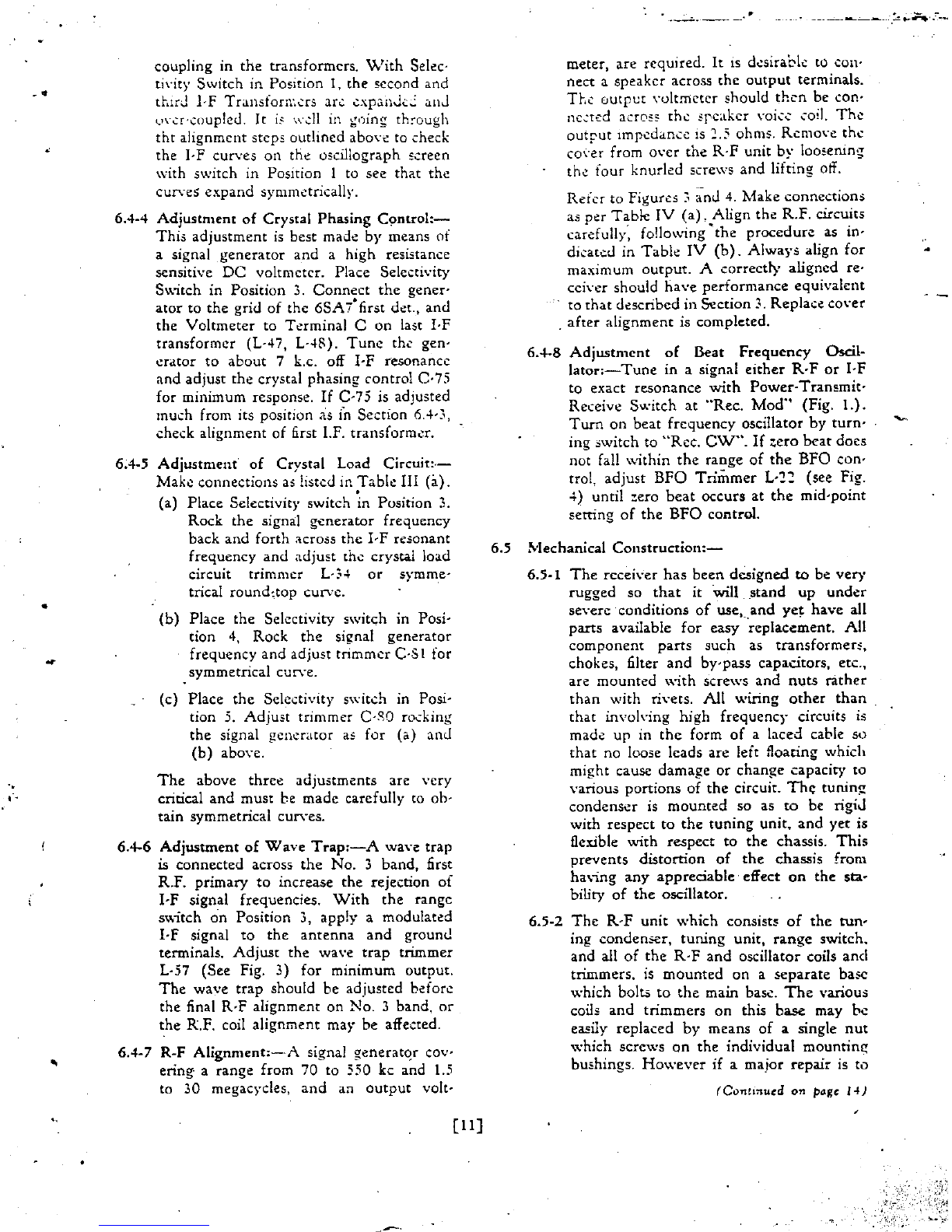
6.4a7
R·F
Alignrnent:-·A
signal
generatqr
cm!-
ering· a range from 70
to
350 kc and
1.5
to 30 megacycles,
and
an
output
volt-
[ll}
..
_._.-----
.:
..:.
.........
;~.
meter, are required.
It
is
d.:sirabk
to con·
nect
a speaker across
the
output
terminals.
Tl-•
.:::
0Utput
\'oltmctcr
should thc-n
be
con-
nc.:tcd across
the
srcakcr
\·oi..:-.:
.:oil. The-
outFut
Impedance is 2.5 ohms.
Rcmo\'e
the
CQ\'er
from
over
the
R·F
unit
by
loosenin~
th~
four
knurled scre'\vs
and
lifting
olf.
Reier
to
Figures
~
~nJ
4.
l-.1ake
connections
as per
Table
IV
(a),
Align
the
R.F. circuits
carefully', follo\ving"
the
procedure
as in-
dicated in
Table
IV
(b).
Always
align
for
maximum
output.
A correctly aligned re-
ceiver should
ha
....
e
performance
equivalent
to
that
described in Section
3.
Replace
CO\'er
.
after
alignment
is
completed.
6A-8
Adjustment
of
Beat
Frequency
Oscil-
lator:-Tune
in a signal
either
R·F
or
I·F
to
exact resonance
with
Power-
Transmit-
Receive
Switch
at
"Ree.
Mod"
(Fig.
I.).
Turn
on
heat
frequency
oscillator
by
turn-
ing
switch to
"Rcc.
CW".
If
:ero
beat
does
not fall
"ithin
the
range
of
the
BFO
con·
trol.
adjust
BFO
Trimmer
L·1:
(see Fig.
4)
until
::ero
beat
occurs at the
mid~point
setting
of
the
BFO
control.
6.5
lvlechanical
Construction:-
6.5·1
The
rccei,'cr
has
been
designed
to
be
very
rugged
so
that
it
-will
_stand
up
under
severe conditions
of
use,.
and
ye~
have
all
parts available
for
easy ·replacement.
All
component
parts
such as transformer.::.
chokes, filter
and
by·pass capacitors, etc.,
are
mounted
with
scrc'ws
and
nuts
rather
than
with
rivets.
All
wiring
other
than
that
invoking
high
frequency
circuits
is
made
up
in
the
form
of
a laced cable so
that
no
loose leads
art::
left floating which
might
cause damage
or
change
capacity
to
yariou5 portions
of
the
circuit. Thl;:
tuning
condenser
is
mounted
50
as
to
be
rigiJ
with
respect
to
the
tuning
unit,
and
yet
is
flexible
with
respect
to
the
chassis.
This
prevents
distortion
of
the
chassis from
having
anr
appreciable effect
on
the
sta·
bility
of
the
oscillator.
6.5·2
The
R~F
unit
which
consists
of
the
tun-
ing condenser,
tuning
unit,
range
switch.
and
all
of
the
R-F
and
oscillator coils
and
trimmers.
is
mounted
on a
separate
base
which bolts
to
the
main base.
The
various
coils
and
trimmers
on
this base. may
be
easily replaced
by
means
of
a single
nut
\vhich scre
.......
·s
on
the
individual
mountin~
bushings.
However
if
a ma.jor
repair
is
tu
(Con!1l1uc-d
on
ptlge
1-4)
".

•
.'
•
'.
.,
..
TABLE No.
IV
(a)
R.F. ALlGNME!,;T CONNECTIO:"'S
~
_,17
Output
Meter
Conncctioi15
Dummr
Antenna
Generator
Modulation
Position
uf
Tone
Control
Position of
Antenna
Trimmer
Position
of
PowerlTransmit~Receive
Switch
..
,
Position
of
Range
Switch ...
~
...
..
Position
of
R·F
Gain Control .........
Position
of
Audio Gain Control
Position
of
Noise Limiter and A
VC
&Witch
Position
of
Selectivity Switch
(..:
-.I"
l!Iorro_)
L.-J~
C,t.-.I.r
4()rrt:lH)
L.
-~"
Cl.-3i!
""""""""')
,,-"'s-
I
L-~tO
•
."
#AA'P
.UIS'
A:'C'.
L,'3
',~(I
-#
......
,0
.(r~'c
~.13
,
~·~I
•
..f_"~
.:tr<J,,'C".
C-7S"
("'JI'JrAL
,,*_J/N#"
C"t:M'T~t:
~-'J'
~
~-'4"
.t!'
.....
""
"".r,t:".
Acruss
I spea.ker
voke
coil
"
r:o-",
.......
4AH~
v.
~t:lg.rr.
c-~_
-.:14"""".17
"fI,.?fd
K'C
L-<!"7"
L-.?'~
-_4A",";
"!
#-(7"
c..,t:~
..
.,..,-.",
/./.
""(7
~C.
c-."
•
...
IAN.:>
~
.i'fd"~
o!-/7
.,.
t:~/4
...
."...""
,-"<1O'C'.
C"-4"
4""
4_~
//..:Jt)~
.rc.
Sce Table
IV
(b) below
.
30~~
at
-wo
cyCles
...
Fully clockwise
See Table
IV
(b)
below
Positi<;n 3 (Ree.· Mod.)
Sec Table
IV
(b) below
Retard to reduce noise
Fully clockwi..::
..
Position 1 (Manual)
... Position 2
~·s_
._
4_~
-er;
.!'sa
,r-c.
~_J"
-.:r'-'-b
Po
JJOD
~C.
C-~?
-r
~p
"'.
fa"
.re
L-.s-~
--~
8A_,::1
/',
ODO"yCo
C"~.4t!'
-to
4_';
jO,
$"oorC"
L-~J~~·~.
..
/,,~~
""~~
~L~.:IO
.$
__
':;;
A<';/J"t7
,~
C".~G
-..1"
4A.Y~
/3,
""0-,",<
Figure
4.-Gener.a1
Purpose
Communications
Receiver-Alignment
Layout
.
[1~]
:
..
' .

.'
•
•
•
'.
,.
p . _ . . .
..;.
1·-
.
~.-.-
._--
-----.-_
. ;
.•
"'--_
...
·r!;.·
______
-=
__
.
.-
.:,:""",
Oper'
atlon
No.
1
2
3
4
5
6
7
8
9
10
11
12
13
14
15
16
17
18
19
20
21
22
23
24
*25
26
27
28
29
.
30
*31
32
33
34
35
36
TABLE No.
IV
(b)
R.F. ALIGNMENT ADJUSTMENTS
Range
Switch
Posi-
tion
Po~ition
of Dial.
and Generator
Frequency Dumm}'
Antenna
1
74
700 mmf
1 200 700 mmf
P05itioa of
Antenna
Trimmer
T:i.=lm.::r
Ad;wt-
r:.<!ots
for
Mu.
Peak Output
(See
figu:oes
1
and
4)
Lo51
C·16
Trimmer
Function
Low
end
OSC.
High
end
osc.
Repeat 1 and 2 until end frequencies are as indicated.
1 195 700 mmf Max.
output
1
80.
700 mmf
Untouched
Repeat
...
and 5 until circuits remain
"in
alignment over the band.
C37,
C59
1st &
2nd
R·P
L.2, L·14, L·24
·Ant.
& 1st and
2nd
RjF
. .
2 200 700
mmf
2 545 700
mmf
Lo52
C·19
Low
end
osc.
High
end
osc. .
Repeat 7 and 8 until
end
frequencieS' are
a.
indicated.
2 500 700
mmf
Ma:<.
output
C·
38,
060
1st &
2nd
R·F
2 205 700 mmf Untouched
L'4,
L·16, L·26
Ant.
& 1st and
Repeat
10
and
11
until circuits remain in alignment over
the
band. 2nd
R·F.
3 1,500 200 ohms
3 4,350 200 ohms
Repeat
13
and
14
until
end
frequencies are as indicated.
3 4,250 200
ohm.
Max.
output
3 1,600 200 ohms Untouched
Repeat
16
and
17
until circuits remain in alignment oyer the band.
4 4,300 200 ohms
4 12,100 200 ohms
L·53
C-2:!
C41,
C·64.
L·6, L·19, L·29
L·54
C25
Repeat
19
and
20 until
end
frequencies are as indicated.
4 11,900 200 ohms Max.
output
C·39, C·62
4 4,400 200 ohms Untouched L·8. L·18, L·28
Repea.t 22 and
23
until circuits remain
in
alignment over the band.
5 12,000 200 ohms
5 19,400 200 ohms L·5S
"C27
Low
end
osc.
High
end OSC.
1st &
2nd
R·P
Ant.
& 1st and
2nd R·F.
Low
end
osc.
High
end
osc.
1st & 2nd
R·F
Ant.
& 1st and
2nd R·P.
Low·end osc.
High
end
osc.
Repeat
25
and 26 until
end
frequencies are as indicated.
S
19,0"00
200 ohms Max. output
C·4:,
C·66
1st <i 2nd
R·F
S 12,150 200 ohms Untouched L·10, L·20, L·30
Ant.
<i 1st
and
Repeat 28 and 29 until circuits remain
in
alignment over
the
band.
2nd·R·F
.
6 19,100 200 ohms
6 30,400 200 ohms
Lo56
c·n Low
end
osc.
High
end
osc.
Repeat
31
and
32
until
end
frequencies are as indicated.
6 30,000 . 200 ohms Max.
output
C45,
068
1st &
2nd
R·P
6 19,500 200 ohms
Untouched.
L·12, L·21, L·31
Ant.
& 1st
and
Repeat
34
and
35
until circuits remain in alignment over
the
band.
2nd
R·F.
*NOTE:
On
all coils, except
Nos.
5
and
6 band
oscillator coils (L'55,
and
L·56) turning
the
core clockwise increases
the
induct·
ance.
On
the
above two mentioned
coils,
turning
the
core clockwise de·
creases the inductance.
.....
'.-
On
all bands
the
oscillator tracks above
the
sig'
nal frequency.
If
more
than
one
peak is obtainable
on
oscillator,
use
the
higher
frequency peak.
[Il]
'~.-..
.
.....
.,"'"

..
"
...
'--<..
......
,.
.......
~."J'.
6.5
Mechanical
Construction(Conllllued
from·
page
J
J)
b..;
ma.Jc
su..:h as
r.:pla..:...:nh.:nt
uf
the
rang
....
s\\.·itch,
it
is
necessary
fir::t
to
remove thL
complete R·F unit from the recei\'er. To
do this the following procedure should be
observed:
(a.)
Remove the chassis and panel
from.
the cabinet
by
removing the four
panel mounting screws and sliding
the chassis forward out
of
th"
cabinet.
(b)
Remove the knobs
by
means
of
th"
small wrench held in
the
spring clip
on
the
right
hand
side
of
the chassis.
This
wrench fits the set screws in
all
knobs except
the
main tuning
kno~.
For this knob use an ordinary small
screw driver.
(c) Remove
the
panel
by
remo,·ing the
eight nuts with which
it
is
held
to
the support brackets.
(d) Remove the large
co.er
from
the
top
of
the
R-F unit, by removing
the
four
knurled nuts with
which
it
is
sup'
ported.
(e) Remove the small cover from the tun-
ing conpenser.
by
removing
the:
eight knurled nuts
with
which it
is
supported.
(f)
Remove the dial light sockets where
they are clipped on to the tuning unit.
(g) Remove the antenna trimmer shaft
extension by loosening set
s..:re\\.'
in
coupling with same wrench
as
used
above for knobs.
(h)
Remo,·e support bracket from
fly-
wh"ei tuning shaft.
(i) Remove main dial, vernier dial. and
[14]
flywheel by loosening set
5crC\"'s
with
same wrench
as
used for knobs.
(j) 'Disconnect the eight leads which con-
nect the R·F unit to the main hase.
These
leads
arc as
follows:-
(if
Two
on the antenna terminal
board--(blue and black).
(ii)
Onc
on number 7 pin
oj
the
6V6GT
IG
output
valve
(brown).
(iii)
One
on tcrminal E
of
the
crystal load cireuit (yellow).
(iv)
One
on terminal E
of
the
first
I-F Transformer
(red).
(v)
One
on terminal F
of
the first
. I-F Transformer (blue).
._.(vi)
One
on pin 6
of
the
second l-F
valve (green).
(vii)
One
on
pin
7
of
the
second I·F
valve (brown)_
In
addition,
the
by-pass condenser
wrueh grounds
to
the
R-F
unit
near
the
second I-F valve must ·be dis-
connected.
(k) Remove eleven screws which hold
R-F
unit
to main base.
Three
of
the>e
arc on under side
of
chassis
along
the
front edge.
The
other
eight ar< re-
moved from
the
top
..
(1)
The
R-F unit may now he rcmo,·eu
from
the
bottom by lifting
ur
first
th"
rcar
of
the R-F
unit
and sliding it
hack
out
of
the
opening.
After
the
unit has been repaired it may
be
r~·
assembled
by
follovdnl! the above
procedure
in
reverse order.
..
(
...
-

',.
•
•
•
,-
•
Schematic
Reference
A·l
C·l
C·2
"'C-3
C-4
C·5
·C-6
C·9
C·ll
C·12
.~:-
-
TABLE
NUMBER
V
PARTS
LIST
C;ENERAL PURPOSE
COMMUNICATION
RECEIVER
Nomen.
DESCRIPTION
RCA
Victor
:
~t:;,:l'
R.C.A.F.
__
d_atu_r_e
___________
---,-_:_------------------
__
M:...;,.f,:";.'
.:.N;,;o.:..--,I
Spu.s
;
__
R_o1_._N_O_'-j
Crystal
735
KC
Cryst.1
&
C.....
MI.19454.2!
1 i
10Xln5
Condenser
4700
mmfd.
:!:
10~,
500V,
(mica)
102899·507
I 3 '
10C:8102
~~~:~::~
~02!1~m~~~.
p~~~.~
..
~~~~nn~
..
~.~~.~.~~
...........,
..
,
...................
, .
253132·2
( 1
lOC/8121
Condenser
220
mmfd.
:!:. 10'l'(,
SOOV,
Temp.
Coeff. -
.00075
mmf./mmf.rC:
90581·341
:2
10C:SQ86
Condenser
Same
as
C-4. .
~~~:~::~
~08~~
·i()~;;:'·si)OV~'·T~~p:·C~fi··=·:ooo·jS"·~j~~fJ.;CI
Condenser
Same
as
Cl
..
Condenser
56
mmfd.
±
10(,""(",
SOOV,
Temp.
Coeff. -
.00075
mmf.!mmf.rC
Condenser
Condenser
Condenser
Condenser
Condenser
Condenser
Condenser
Condenser
Condenser
Condenser
Condenser
Condenser
U
ondenser
Condenser
Condenser
(mdenser
:
Condenser
I
Condenser
Condenser
(ine.
in
L-5"1). ............ .................,.'
Same
as
c.4..
.................. ......................................
Same
as
C-4...............
..................... ........
47
mmfd.
±
5~",.
SOOV,
Temp.
Coeft'. -
.00015
mmf./mmf.rC
Air
trimmer
2.20
mmfd...
. .
....
,.......
68
mmfd.
:::
S'7c,
SOOV.
(mica)
..............,.......................................
39
mmfd
.....
Sf;'I-,
500V,
Temp.
Coe:l.
-
.00012
mmf./mmf./~C
Air
trimmer
2-12
mmfd......
. .................... .
.....................
.
240
mmfd.
±
50/0,
SOOY,
(mica)..
.
.............
.
15
mmfd.
±
So/c,
500V,
Temp.
Coeff. -
.00047
mroiJrnmf.rC.
Air
Trimmer
-
Same
aa
C·19
.........................
.
1000
mmfd.
±
51/",
37SY,
(mica)
2500
mmfd.
±
So/c,
SOOY,
(mica)
I
Air
Trimmer
-
Same
as
C·19
.
Same
as
C~21....
. . ..............
"1
Air
Trimmer
2~2'5
mmfd.
.....
..................
.
3000
mmfd.
::t:
5%,
500V.
(mica)
..........................................
.
30
mmfd.
±
S~1(,
SO(fV,
Temp.
Coef!'. -
.00047
mmf./mmf./cC
3900
mmfd.
:1:
S~.
SOOV.
(mica)
I
39
mmfd.
:!:
5~(.
SOOV;
Temp.
CoeH. -
.00041
mmf
..
:mmf./cC
i
905S1·309
1
90581·327
90577·225
1
95534·502
2
72053B·39
I
90574·223
1
95534-503
1
720538·32
1
905S0·213
1
721133-4
1
721133·24
1
95534·501
2
721133·12
1
90580·220
1
720538-46
I
1.
90580·223
.• 1
lOC/80S7
10C/S093
10C/SllS
10C/8ll1
toC/B092
IOC/8ll9
10C/8105
10C/8094
IOC/8ll4
10C/8116
10C/8120
toC/8llS
IOC/8099
10C/8112
10C/809S
C·l3
C·14
C·15
C·16
C·17
C·18
C·19
C·20
C·21
C22
C·23
C·24
C·25
C·26
C·27
C2B
C·29
C.30
C·31
C32
C·33
C34
·C·35
C36
C·37
C3B
C·39
C:C-40
I
Condenser
-
-'-1
1
Condenser
Condenser
Condenser
Condenser
I
Condenser
i
Condenser
~~~r!:C.e{.~.~.~~.~
..
~~.~~~~.::
................,....,
.....................
,.,....... :
..
1
ll;l§:~iii£~~i~.~~ie~).·
...
·.·
..
···
..
·
...
·
..................
I 9B041·1 I
lOC/8100
C-41
C-43
C·44
C-45
C-46
C-47
C-48
·C-49
·C·50
C51
C52
C53
C54
C·55
C.S6
C57
C58
C59
C-60
C-61
C-62
C-63
C·64
C-66
C-6i
C-68
C-69
·C·70
C-71
cn
C.73
C.7S
C·76
\
Condenser
Condenser
I
Condenser
1
Condenser
j
Condenser
,
Condenser
Condenser
Condenser
Condenser
Condenser
Condenser
Condenser
Condenser
Condenser
Condenser
Condenser
Condenser
Condenser
Condenser
Condenser
Condenser
Condenser
.\
Condenser
•
Condenser
Condenser
Condenser
Condenser
Condenser
Condenser
Condenser
Condenser
Condenser
Condenser
Condenser
Condenser
I
Air
Trimmer
-
Same
as
C~16..
..... I
Air
Trimmer
-
Same
as
C·16
.......................
8·128
mmfd...
. .... .......... '. i
Air
Trimmer
-
Same
as
C~16..
.... .............. . I
Air
Trimmer
-
Same
as
C·27
.........................................................
I
6.8
mrofd.
==
10(,(,
SOOY.
Temp.
Coeff. -
.00075
mmf.!mmf.rCI
Air
Trimmer
-
Same
as
C-27..
. . . .................... . \
~:::
:5
5
c:i~.~·
.
:::
'.:::::
.:::::
.....
:::::::::
:::'.::::
::.'.::~:
...
:::::::
'.'.:
'.:'::::
,I
.05
mfd.,
400V,
(oil
filled)
(C·48,
C·109,
C-UO.
in
one
assembly):
~O:~~Om::!Id.
.
..
·
..
·....·..1
Same
as
C·l..
............................................
Same
as
C-l..
..............................
Same
as
C-44
..... .
Same
as
C-l
......,......... ...... .....,...................................
390
mmfd.
±
Slfi-.
SOOV,
(mica)
(included
in
T~3)
.........................
.01
mid.,
400V.
(oil
filled)
(C-56,
C~76.
C-93,
in
one
as.sembly)
....
Same
as
C4
...............................................,.................................,........
Same
as
C-36..... .......................
Air
Trinuner
-
Same
as
C-16... .............. ................. ....................
.1,
Air
Trimmer
-
Same
as
C-16........ . .................
Same
as
C-9
................ ...................
Air
Trimmer
-
Same
as
C-16
.................................................
..
Same
as C·I.................................... . ..................
Air
Trimmer
-
Same
as
C·16
..................................
Air
Trimmer
-
Same
as
C-21................................. ..............
22
mmfd.
==
10'li-,
SOOV,
Temp.
Coeff. -
.00015
nunf./mmf./:C.
Air
Trimmer
-
Same
as
C-27
....."...............................
Same
as
C46....
..............,..........................................
8·12S
mmfd.
...
......
...
..
......._................
..
U.l
mfd.,
400V,
(oil
filled)
(C-71,
C-95,
C-I02,
in
one
assembly)
I'
Same
as
C-SS
(included
in
T·3)
....................................................... :
100
mmfd.
±
5'70.
500V.
(ine1uded
in
T-4)
(mica)
..
3-15
mmfd.
Crystal
Pha!l~g
Trimmer
.01 mId.
400V
(lee
C·56)
. .
[17]
905S1·305
1
98034·1
86079·505
98034-4
90581·317
98034-2
86034-522
253132-6
1
10C.·8088
10C'S083
10C/80S4
lOC.·8090
IOC/S085
IOC'8123

.-
SchematiC
Rlderenee
'::C·7i
C-78
C-79
C·SO
C·81
C·82
C-83
C·84
C·85
C·86
C-S7
C-88
C·89
C·90
C-91
C·92
C·93
C-94
C·95
C·96
C·97
C-98
C·99
C-IOO
C·IOI
C-I02
C-I03
C·I04
C·I05
C·I06
C·I07
C·IOS
C-I09
C-110
C-lll
C·1l2
C-1l3
C·1l4
C-II5
C-1I6
C·II7
C-llS
C·1l9
C·121
C·122
C·123
C·124
C·125
C·126
C-127
C-128
C·129
C-130
.,
NOTE:
F-1
J.I
J.2
L-1
L-2
L·3
L-4
L-5
L-6
L-7
L-8
L-9
L-IO
L-II
L·12
L-13
L-14
L·15
L-16
TABLE NUMBER V - PARTS LIST
rContinuedl
Nomen-
DESCRIPTION
ReA
Victor
~h"
of
clature
Mf!!:;.
No.
s
......
------------------------------
---==::.-.:..:.:;-
-~~
Condenser
Condenser
Condenser
Ccndenser
Condenser
Condenser
Condenser
Condenser
10·370
mmtd.
Same
as
C-SS
(included
in
T.5).
0.1
mid
..
400V,
(oil
filled)
(C-79,
C-84.
C-92,
in
one
assembly)
Air
Trimmer
-
Same
as
C-16
._._
.... ",., ".
_"
..
,.,
.__
""
..
Air
Trimmer
-
Same
as
C-16
.
56
mmfd.
::::
5'"
SOOV,
(mica,)
(included
in
T-IO)
Same
as
Col
0.1
mfd
..
400V,
(See
C-79).
330
rnmfd.
::t:
20';,
SOOV,
(mica)
(included
in
T-IO)
3-15
mmfd.
B.F.Osc.
Panel
Trimmer.
1500
mmfd.:!:
10(;"
SOOV.
(mica)
(included
in
T-IO).
Same
35
C-82
(included
in
T-IO)
Same
as C-5S
(iniluded
in
T
-5)
,.
Same
as
C·S5
(included
in
T
-6J.
Same
as C-5S
(included
in
T
-6)
0.1
mfd.,
400V,
(See
C-79).
0.1
mid.,
400V,
(S
..
C-56)
Same
as
C-S5
(included
in
T-7)
..
0.1
mfd
.•
400V,
(See
C-71)
..
.~'
..
.
.. ..
I
.
····1
....
1
.
..........
I
.....
.......
i
i
Condenser
Condenser
Condenser
Condenser
Condenser
Condenser
Condenser
Condenser
Condenser
Condenser
Condenser
Condenser
4
mfd.,
+
20~;'i:
-107c,
Dry
Electrolytic
(C-96,C-97,C-98
in
one
assembly)
...i
Condenser
4
mfd
..
+
20
f
;.
-10'7;',
Dry
Electrolytic:
(See
C-96)
.
I "
Condenser
. 4
mfd.,
-:-
20~'~
-10'7<,
Dry
Eleetrolytic
(See
C.96)
. I
Condenser
.25
mfd.,
400V.
(oil
filled)
(C-99.
C·U2,
C-113,
in
one
assembly)
I
Condenser
Same
as
C·S5
(included
in
T-7).
..... ......... . !
Condenser
Same
as
C·SS
(included
in
T
-8).
Condenser
0.1
mfd
..
400V,
(See
C·7!") ........... ..... ......... .
.............
.
Condenser
.05
mid
..
400V,
(oil
filled)
{C-ID3,
C-ID6,
C-ID7,
in
One
assembly
Condenser
Same
as
C-55
(ineluded
in
T
-8)
....... ..... 1
Condenser
560
mmfd.
±
10r(.
SOOV,.
(mica)
.....
Condenser
.05
mid
..
400V,
(See
C-I03)
Condenser
.05
mid.,
400V,
(See
C-I03)
Condenser
Same
as
C·73
(included
in
T-9)
...
Condenser
.05
mid.,
400V.
(See
C-48).
Condenser
.OS
mid.,
400V,
(See
C-48)
'''1
..............
,
Condenser
2700
mmfd.
± 10'-"
SODV.
(mica)
Condenser
.25
mfd
..
400V.
(S~
C-99)
Condenser
.25
mfd
..
400V"JSee
C-99)
Condenser
Same
as
C-73
(inl:luded
in
T-9)
..
Conden!oer
180
mmfd.
± 5r
;.,
500V,
(mica)
(included
in
T-9)
Condenser
Same
as
C-Ill
Condenser
Same
as
C-l..
.................. .
Conqenser
Same
as
Col
..............
.
Condenser
.003
mfd.
--
10',.
1000V,
(.oil filled)
Condenser
Same
as
Col
Condenser
Same
as
C-l
Condenser
Same
as
C-4
Condenser
150
mmfd.
=
10'~.
SOOV,
Temp.
Coeff. -
.00075
mmf./mmf./°C
Condenser
650
mrnfd.
±
10'
(,
300V.
(mica)..
.
Condenser
Same
as
C-12S
Condenser
Same
as
C~20
Condenser
285
mmfd.
=5'.1,
500V,
(mica)
Ccndenser
Same
as
C-9
Condenser
Same
as
C-ID5
... .
.............................................
.
C·l,
C.6,
C·lS,
C·40, C·44.
C·SO,
C·70,
C-77,
all
part.
.f
Fuse
Socket
Jack
Coil
Coil
Coil
Coil
Coil
Coil
Coil
Coil
Coil
Coil
Coil
Coil
Coil
Coil
Coil
Coil
(V~~~aa~~.;O~d~~si:r
A~'~::I.y
.........................
..
"1
1
Connection.
for
battery
operations
............... ................... "'1
Jack,
phone
...........................
..
..........1
Antenna
Prim.
73-205
KC
(L-l
&:
L-2
on
same
coil
form)
"
Antenna
Sec.
73-205
KC
(See
L-l).
..
...............
·.1
Antenna
Prim.
195-550
KC
(L-3
&
L-4
on
same
coil
form)
:
Antenna
Sec.
195-550
KC
(See
L-3).
......
........
......i
Antenna
Prim.
1~80-4400
KC
(L-S
&
L-6
on
same
coil
iorm)
i
Antenna
Sec.
1~S0-4400
KC
(See
L-5).
Antenna
Prim.
4250-12150
KC
(L-7
& L-S
on
same
ceil
form)'"
i
Antenna
Sec.
4250-12150
KC
(See
L-7)
...
Antenna
Prim.
11900-19500
KC
(L-9
&:
1.-10
on
same
coil
form)
Antenna
Sec.
11900-19500
KC
(See
L-9)
Antenna
Prim.
19000-30S00
KC
(L-ll
&.
L-12
on
same
coil
form)
Antenna
Sec.
19000-30500
KC
(See
L-ll)
........................
.
1st
R.F.
Prim.
;3-205
KC
<L-13
&:
L-14
on
same
coit
form)
1st
R.F.
Sec.
73-205
KC
(See
L-13).
1st
R.F.
Prim.
195-550
KC
(L-15
&
L-16
on
same
coil
form)
...
1st
R.F.
Sec.
195-550
KC
(See
L-lS)
[18]
9S034.2
861)34.517
86034·524
253132-7
86034-54S
72026-515
98034·3
98034·1
100404-528
102899-508
86034-513
251248·3
90581.337
720592·13
720538-31
92444-502
55544-2
421395·509
98965-3
253674-506
253674-507
95521·501
95521-502
95521-503
253671·505
253674-501
253674-502
I
I
I
I
I
I
I
1
8
2
R C.A.F.
Re{.
No.
lOC/8085
IOC/SI24
IOC/8081
IOC/S082
'.
10C'8083
IOC/8101
IOC/8103
IOC/B1l7
IOC/8091
10c.-S1l3
IOCi8104
IOe/8122
5Cil705
IOH/8168
10H/8185
IOCl
8142
lOC/S143
10C
'S144
IOC.8145
10C/S146
IOC/8147
IOC/8H8
IOC.'8149

•
•
_l
•
..
Schematic
Refere-nee
Nomen.
c1ature
TABLE NUMBER V - PARTS LIST
IContinued'
DESCRIPTION
ReA
Vietor
W;;::
R.eA.F.
Ref.
So.
_
__________________________
Mfg.
No.
Spare-s
/---------
---'---
--
---
L-17
1.-18
1.-19
r;20
1.-21
1.-22
L-23
L-24
L-25
1.-26
1.-27
1.-28
1.-29
1.-30
L-31
1.-32
1.-33
1.-34
1.-35
1.-36
1.-37
L-38
1.-39
1.-40
1.-41
1.-42
r;43
1.-44
1.-45""
1.-46
1.-47
1.-48
1.-49
1.-50
1.-51
L-52
1.-53
1.-54
1.-55
1.-56
1.-57
L-60
1.-61
P-I
P-2
R-I
R-2
R-3
R-4
R-5
R-6
R-7
R-9
R-IO
R-l1
R-12
R-13
R-14
R-15
R-16
R-17
R-19
R-20
R-22
R·:23
R-24
R-25
R-26
R-27
R-28
R-29
R-30
R-31
R-32
Coil
Coil
Coil
Coil
Coil
Coil
Coil
Coil
Coil
Coil
Coil
Coil
Coil
Coil
Coil
Coil
Coit
Coil
Coil
Coil
Coil
Coil
Coil
Coil
Coil
Coil
Coil
Coit
Coil
Coil
Coil
Coil
Coil
Coil
Coil
Coil
Coil
Coil
Coil
Coil
Coil
Coil
toil
Plug
Plug
Resistor
Resistor
Resistor
Resistor
Resistor
Resistor
Resistor
Resistor
Resistor
Resistor
Resistor
Resistor
Resistor
Resistor
Resistor
Resistor
Resistor
Resistor
Resistor
Resistor
R,esistor
Resistor
Resistor
Resistor
i'
Resistor
Resistor
Resistor
Resistor
Resistor
..
.
..
1st
R.F.
Prim.
4250-12150
KC
(L·17
&
L-lS
on
same
coil
(orm)
1st
R.F.
Sec.
4250-12150
KC
(See
L-17)
1st
R.F.
Sec,
1480-4480
KC
(L-19
& L-61
on
same
coil
form)
1st
R.F.
Coil
11900-19500
KC
lst'
R.F.
Coil
19000-30500
KC
B.F.
Dsc,
Coil
(See
T-10)
2nd
R.F,
Prim,
73-205
KC
(L-23
&
L-24
on
same
coil
form)
2nd
R.F.
Sec.
73-205
KC
(See
L-23).
2nd
R.F.
Prim.
195-550
KC
(L-25
&
L-26
on
same
coil
form)
2nd
R.F.
Sec.
195-550
KC
(See
L-25).·
2nd
R.F.
Prim.
4250-12150
KC
(L-27
&
L-28
on
same
coil
fonn),
2nd
R.F.
Sec.
4250-12150
KC
(See
L-27)
, ... ,
..
,
.........
""."."
..
2nd
R.F.
Sec.
1480-4400
KC
(L-28
&
L-60
On
same
coil
fonn)
2nd
R.F.
Coil
11900-19500
KC,.
..........................
~.
2nd
R.F.
Coi119000-30500
KC
.
I.F.
Trans.
Prim.
(See
T-3)
..
I.F,
Tram.
Sec.
(See
T
-3)
.
Crystal
Selectivity
Coil
(See
T
-4)
I.F.
Tranlj.,
Prim.
(See
T·5)
.............
I.F.
Trans.
Sec.
(See
T-5)
....
..
I.F.
Trans.
Prim.
(See
T-6)
.....
I.F.
Trans.
Sec.
(See
T-6)
..
Variable
Selectivity
Coil
(See
T-5)
Variable
Selectivity
Coil
(See
T-6)
..
I.F.
Trans.
Prim.
(See
T·7).
I.F.
Trans.
Sec.
(See
T-7)
.....
I.F.
Trans.
Prim
.•
(See
T
-8)
..
I.F.
Tral'ls,
Sec.
(See
T-8)
."
..............
..
Variable
Selectivity
Coil
(See
T-7)
..
Variable
Selectivity
Coil
(See
T-8)
I,F.
Tuns.
Prim.
(See
T-9).
I.F.
Trans.
Sec.
(See
T-9)
..
Filter
Choke
....
Filter
Choke
-
Same
as
L-49.
Oscillator
73-205
KC
...
Oscillator
195-550
KC
Oscillator
1480-4400
KC
Oscillator
4250-12150
KC
Oscillator
11900-19500
KC
................. .
Oscillator
19000-30500
KC
..
I.F.
Wave
Trap
(includes
C.12)
2nd
R.F.
Prim.
1480-4400
KC
(See
1,..29)
1st
R.F.
Prim.
1480-4400
KC
(See
L-19)
..
AC
Power
Plug
&
Cord
................
in
J-1
for
normal
AC
operation
..
33,000
ohms
±
10~{
1J2
W...
2.2
meg.
::::
20,;!
1/2
W...
1,000
ohms':::
10{ic
1/2
W.
100.000
ohms
:t:
10(1c-
1J2
W.
LO
meg.
± 20t;(
1/2
W ...
Same
as
R-1............. .............. .
.
330
ohms
±
10%
V2
w.................
..
r
Same
as
R-4..
..
........................
..
1
Same
as
R-3..
. .................
10,000
ohms
::!:
1Of/~
1f2
W.
..
........................
,
I
I
.....
!
,
";
I
·
Same
a.
R-3..
.
........
" .................
····.1
560
ohms::
10%
'(2
Wo..
.
....................
::
......................
.
Same
as
Roo4
........................................................................................
·1
,
22,000
ohms.:::
10%"112
W.
(included
in
T-3)....
. .....................
i
Same
as R-3.........
..
..........................
I,
Same
as
R-7.... ..................
Same
as
R-l..
.
..
................
..
.....
1
!
100
ohms
.....
10
f
ic
1/2
W
..
.
Same
as
R-3
.....
..
560,000
ohms
±
1O
f
:i
'11
w
......
120,000
ohms
lOf
l,
~~
W.
(included
in
T
.10)
...
47
ohms
± 10(ii %
W.
Same
as
R-3
...............
..
Same
as
R-23
.
Same
as
R-24
(included
in
T-10)..
..
.............
.
47,000
ohms
:::
10';,
1/2
W.
(included
in
T-IO)
!
2.700
ohms
± 10tJc 4 W.
Same
as
R-3
390
ohms
:::-
1O~;,
% w.
[19]
I
.•
~.
253674-508
95520-503
253671-501
253671-502
253674-501
253674-502
253674-508
95520-503
I
2536il-501
253671-502
901433-501
253674-503
253674-504
95520-506
253674-505
253671-503
253671-504
253481-502
,
811638-1
99895-501
850981-80
850981-33
82283-62
82283-86
82283-31
82283-56
82283-74
850981-59
82283-7iI
82283-50
82283-95
82283-87
82283-46
82283-82
90497-3
850981-57
I
1
I
1
I
2
I
I
1
1
I
1
2
I
1
loc/al50
IOC/8151
10C.·8152
10C.8153
IOC/8148
10C/8149
IOC/8150
IOC/8151
IOC/8152
10Ci8153
10C&154
10C/S1SS
10C/8156
IOC/8157
10C
'8158
IOC.'8159
10C
'8160
10C
8161
10H8184
10C
8134
10C
8131
lac
'1673
IOC'3281
10C'5750
lOC
'7729
10C/1675
10Cl7259
IOC
'3260
IOC'M88
IOC"7747
IOC/8128
10C
'7282
-

.
TABLE
NUMBER
V -
PARTS
LIST
'Contlnuedl
Schl!:natic
Nomen-
ReA
Victor
,Qt)'.of
I
DESCRIPTION
. N
...
!
I'
R.C.A.F.
Rei.
No.
Reference
clature
Mfg.
No.
Sp.~
----
------------------
--"---
-'--1'·---1
R-33
R-34
R-35
R-36
R-37
R-38
R-39
R-40
R-41
R-42
R-43
R-44
R-45
R-46
R-47
R-48
R-49
R-50
R-51
R-52
R-53
R-54
R-55
R-56
R-58
R-60
R-61
R-62
R-63
R-64
R-65
R-66
R-67
5-1
5-2
5-3
S-4
5-5
S-6
5-7
S-8.
5-9
5-10
S-l1
S-12
5-13
5-14
S-15
5-16
5-17
5-18
5-19
5-20
5-21
5-22
5-23
5-24
5-25
T-I
T-2
T-3
T-4
T-5
T-6
T~j
T-8
T-9
T-IO
TB-I
TB-2
TB-4
V-I
Resistor
Resistor
Resistor
Resistor
Resistor
Resistor
Resi!Stor
Resistor
Resistor
Resistor
Resistor
I
Resistor
!
Resistor
1
Potentiomater
I
Resistor
i
Potentiometer
I
Resistor
Resistor
I
,
Potentiometer
Potentiometer
Resistor
!
Resistor
i
Resistor
!
Resistor
1
Resistor
,
Resistor
Resistor
Resistor
Resistor
Resistor
Resistor
Resistor
Resistor
Switch
Switch
Switch
Switch
5witclJ
Switch
Switch
Switch
5witclJ
Switch
Switch
Switch
Switch
Switch
S\\,-l.tch
Switch
Switch
Switch
Switch
Switch
Switch
Switch
Switch
Switch
Switch
Transformer
Transformer
Transformer
Transfonner
Transformer
Translonner
Transformer
Transformer
Transformer
Transformer
Term.
Bd.
Term..
Bd.
Term..
Bd.
Valve
Same
as
R-2
Same
as
R-3
680,000
ohms
==
10';'{ 1/2
W.
Same
as
R-2
.
LO
meg.
±
20'!,
Vl
W
..
1.5
meg.
±
10%
112
W.
Same
as
R-20
.
270,000
ohms:±:
109(;
"1/::
W.
100,000
ohms
±
10'/",.
1.4
W
..
390,000
ohms
:!:
lOo/<
1f2
W.
100
ohms::::!;:
10%
4 W .....
150
ohms
±
10%
4 W..................
15
ohms
±
10%
~
W......................
66,000
ohms
R.F.
Gain
Control..
Same
as
R·2.
..... .
..
Same
as
R-46
(Noise
Limiter
Control)
Same
.1
R·1
...
Same
as
R·23
..
,
...........
.
2.
meg.
Audio
Gain
Control
1
meg.
Tone
Control...
330,000
ohms:::!:
10%
tAt
W.
2,700
ohms
±
10%
1h
W
..
.
6,800
ohms
±
100/'0
¥2
W
..
.
'39
ohms
±
10%
4 W ....
5,600
ohms:±:
10%
1f:z
W•...
Same
as
R-S8
..
......................
Same
as
R·25
..
.... ............... ......................
........
····••••••·•··•·••••••••
•••
1
...
.........
i:::::
5:~t
.:.:::.::.....
···
..
················:1
Same
as
R-23
. .... ............ , ;
Same
as
R-54
I
Same
as
R·S4
I
Range
Sw.
Wafer
Oscillator
Ccts.
(S.1
&.
S-2
on
same
wafer).
~~
Range
Sw.
Wafer
Oscillator
Ccts.
(See
5-1)..
..
Rang.
Sw.
W.fer
Oscmator
Cm.
(S·3
&;
S-4
on
same
wafer)
Range
Sw.
Wafer
Oscillator
Ccts.
(See
S·3)........
.
............
.
Range
Sw.
Wafer
2nd
R.F.
Ccts.
(5·5
&
8-6
on
same
wafer)
Range
Sw.
Wafer
2nd
R.F.
Ccts.
(See
5-5)
..
Range
Sw.
Wafer
2nd
R.F.
Ccts.
(5-7
&
S-8
on
same
wafer)
Range
Sw.
Wafer
2nd
R.F.
Gets.
(See
8-7)
.......
::'1
Range
Sw.
Wafer
1st
R.F.
Ccts.
(8-9
&:
10
on
same
wafer)
...
Range
Sw.
Wafer
1st
R.F.
Ccts.
(See
8-9)
......... . I
Range
Sw.
Wafer
1st
R.F.
CCts.
(5-11
&;
12
on
same
wafer)
..
Range
Sw.
Wafer
1st
R.F.
ern.
(See
S-11).
Range
Sw.
Wafer
Antenna
Ccts.
(S-13
&.
8-14
on
same
'~~i~~)"!
Range
Sw.
Wafer
Antenna
Ccts.
(See
S-13)
....
Range
Sw.
Wafer
Antenna
Ccts.
(S·15
le
8-16
on
same
wafer):
Range
Sw.
Wafer
Antenna
Ccts.
(See
S-15)
..
NOTE:
S·l
to
5-16
includ&d
all
on
one
assembly
....
Crystal
Sw.
WaIer
(5-17
&;
S-18
on
same
wafer)
i
I
Crystal
Sw.
Wafer
(See-
8-17)
.......................
.
Crystal
Sw.
Wafer
(5-19
&; 5020
on
same
wafer)
..
..
••.•••.. 1
Crystal
Sw.
Wafer
(See
8-19)
...... .....................
..
NOTE:
S-17-18.19~20
all
on
same
assembly
..................
A.V.C.
-
N.L.
Switch
Wafer
(8-21
&.
8-22
on
same
wafer)
..
A.V.c.
-N.L.
Switch
Wafer
(See
5-21)
........
Off-Trans.·B.F.O.
Switch
Waier
(includes
S~24).......
..............
On/Off
Toggle
Sw.
(5
..
5-23)
........................................
.
D.P.
D.T.
Line
voltage
Switch
..
Power.
115/230
V.
25-60
cy<le .... .......... i
Output
2.5
ohms
&;
20
ohms...
..
..... ...... .
...........
/
1st
I.F.
(includes
L-32.
1-33.
C-55,
c·n,
R.1S)
735
KC
I
I.F.
Crystal
Load
(includes
L-34
&;
C-73)
735
KC
:::
I
2nd
I.F.
<Includes
L-35, L-36, L-39,
C-78,
C-89)
735
KC
.........
,'
2nd
I.F.
(Include.
L-37, L-38,
lAO,
C-90,
C-91)
735
KC
.,
3rd
I.F.
(Include.
lAl,
lA2,
lA5,
C-94,
C-lOO) 735
KC
...... 1
3rd
I.F.
(Include.
lA3,
L-44,
lA5,
C-IOI,
C-I04)
735
KC
4th
I.F.
(Includ
..
lA7,
lA8,
C-I08,
C-114,
C-115)
735
KC
....
:
B.F.
O.
(Inc.
L-22,
C-82, C-85. C-87,
C-88,
R-24,
R-28,
R-29)
735
KC'
Antenna
&;
Ground.
3
term
...................................................................1
5
Term.
......................
Ou~utforezternalspk.2ternL
Ist
R.F.
A~ifier
PO}
...--',
850981-96
85MSI-31
850981-100
850981-91
850981-86
82283-93
i
90497-1
90497-6
867970-340
251402-2
251402-3
251402-1
82283-92
850981-67
850981-72
90497-7
82283-71
253660-1
I
253134-1
253099-1
253098-1
I
!
252657-1
1
901602-501
i
901611-501
1
255401-501
i
255401-505
i
255401-5031 i
255401-503l
'
255401-503j
i
255401-503
'
255401-502
255401-504
253669-2
253669-1
253669-3
6SG7
I
I
1
I
I
1
1
I
I
I
I
I
1
I
I
I
1
1
I
I
I
1
I
I
I
lOC/8137
IOC/1651
10C!1921
IOC/8136
IOC/8135
IOC/8027
IOC/8127
IOC/8129
IOC/8138
IOC/8139
IOC/8140
IOCl8141
IOC/8126
IOC/8132
IOC/8133
IOC/8130
IOC/8125
10F/8167
IOF/8165
IOF/8166
10F/8163
IOF/8164
IOA/8173
10A/8174
IOA/8175
10A/8176
10A/81;7
10A/8178
IOA/8179
-_..
_-_
..
_---_._-- -
----_
.
......
-,
.....
(
•
•
{
•
-_.:;.-'-

•
'.
.
Schematic
"10
Reference
V-2
V-3
V-4
V.5
V·6
V-7
V-8
V-9
V-IO
V-1l
V-12
V-13
V-14
V-16
X-I
X-2
X-3
X-4
X-5
X-6
X-7
X-8
X-9
X-IO
X·11
X-12
X-13
X-14
X-16
.~
" -
TABLE NUMBER V - PARTS LIST
IContinuedl
Nomen-
DESCRIPTION
ReA
VNictor
I
W:;::
I R.C.A.P.
_--:c::I._t~u,_e
__
-:--:-:::-::--:---::7
______________________
M_f,;;._'_o_·
__
l~,s,"p"':':"'~'I
__
R_
..
_._N_o_,_~
Valve
2nd
R.F.
Amplifier
65G7
Val
....
e
Master
Oscillator
6J5
,.
Valve
1st
Detector,
'Converter
.
6SA7
6
Valve
1st
I.F.
Amplifier
6SG7
,'f
Valve
2nd
I.F.
Amplifier
65G7
12
Vat
....
e
3rd
I.F.
Amplifier
68G7
Valve
2nd
Detector
& A.V.C. ....... ...... ...........
..
......
6H6--
I
Valve
Noise
Limiter
6H6
10£/8188
8
Valve
1st
A.F.
Amplifier
68J7
Valve
Output.
6V6GT/G
6
6
Valve
B.F.
Oscillator.
,_............ . ....... .... ........ .
6J5
Valve
Voltage
Regulator..
VR-1S0
8
6
10£/4298
Valve
Rectifier
.... ....................... . ...............
SY3GTIG
6
Valve
Gas
Gap
Protector.
991
4
10£/6827
Socket
Tube
socket
for
V.;
421395-507
Socket
Tube
socket
faT
V·2
Same
as
X·1
..................... 1
10H/8169
Socket
Tube
socket
for
V-3 . 421395-508 1
IOHl8170
Socket
Tube
socket
for
V
-4
Same
as
X-3
..
Socket
Tube
socket
for
V-S Sa.me as
J-1
Socket
Tube
socket
for
V-6
Same
as
J-1..
Socket
Tube
socket
for
V-7
Same
as
X-1..
Socket
Tube
socket
for
V·S
Same
as
X-I..
Socket
Tube
socket
for
V-9
Same
8S
X-3
..
Socket
Tube
socket
for
V·lO
Same
as
J-l
...........................
..
Socket
Tube
socket
for
V-U
Same
as
X-I
...................
..
Socket
Tube
socket
for
V-12..
..
.....................
..
421395.510
1
IOH!8171
Socket
Tube
socket
for
V-13
Same
as
J-1..
.
...........
..
Socket
Tube
socket
for
V-14
Same
as
)-1
..........1
Socket
Tube
socket
for
V-16
..............."...."........!
837884-2
Board,
Resistor
....................
98958-1
Board.
Terminal
assembly
2
Way
81641-23
Board,
Terminal
assembly
1
Way......
81641-32
Board,
Terminal
assembly
1
Way
vertical
81641-57
~~~~~~~g
assembly
..
~.~~~
..
~.~~~ng
.~~~~.~~.
:.....
'.1
~~g~g=iOl
Coupling
....................... .........................
99630-1
Caps
-
Shield
Can.
................... ........................... I
99840-1
Dial
Assembly........................
.......................................
98947-503
r
I
10H
l
81i2
Fuse
Holder
................... ..........................................
844027-2
Knob
(Large)
..................... ........................
712336-503
Knob
(Medium)
. . ... ............
712336-505
Knob
(Small)
.......................... ..............
712336-507
MISCELLANEOUS
IOA/8187
SC/1304
10A/8180
10A.'8181
10A
l
8182
C-I
C·2
C-3
C-4
CoS
C-6
C-7
C-8
CP-l
F-l
L-I
L-2
P-I
R-I
S-I
S-2
T-"!
TB-I
V-I
VS-l
X-I
X-2
Lamp
-
Pilot
1J.
Amp.
6V
..
......................... ............. .
61114·15
12
Screw
-
Knurled
Thumb
..
_._............ .................
252664-1
Screw
-
Thumb
... ...... ..............
99610-9
Screw
-
Set
#
8-32
for
small
knob
844365-12
Screw
-
Set
#8·32
for
medium
knob
844365-13
Screw
-
Set
# 10-32
for
large
knob
59101-6
I
Socket
Pi1c:t La:mp
(com~lete)
....... .............
98983-501
l
Tool
-AII'
Tnmmer
Ad).
....... ................
81059-501
\
i::
=
~;t
tc~!~
Wre'n'ch .::.:::::::::.....
..
.....:::::::::::::::::::::::.............
8~~~~t~~1
I
Tuning
Unit
...... .................. ............... ................. ....................
92417·1
Vernier
Assembly.....
. ........................................... .............................
98947·502
TABLE NUMBER
VI
-PARTS LIST -
Vibrator
Power
Supply
Unit
110'11.222151
Condeniier
I 0.5
mid.,
::!:
10
l
;',',
120
volts
·
..
-........i
114125-5
Condenser
,008
mfd.,
==
10<;":"
2000
volts
..
I
114125-6
Condenser
I .05
mid.,
==
10%.
600
volts
........... . . ............................
114125-7
Condenser
I 0.1 mid" ± 10Q",
600
volts.
114125-8
Condenser
I
500
mmfd.,
==
10%.
600
volts
(mica)
.'...
114125-9
Condenser
I
Electrolytic,
10
mfd
.•
450
volts.
............ ......... .
114125-10
Condenser
!
Electrolytic,
25
mfd
.•
40
volts.
..
. I
114125-11
Condemer
i
Same
as
C-S "!
Cable
Power
Cable,
includes
P-1,
S·1
Fuse
Type
3
AG,
20
Amperes
..
Coil
Filter
Choke
(iron
core)
Coil
I
Filter
Choke.
Plug
8
prong
octal
plug
(on
CP-!)
Resistor
5,000
ohms,
=
10<!e,
1/4
Watt
Switch
ON·OFF
Switch,
D.P.S.T.
(~n
CP-l)
........................
..
Switch
i
Voltage
Tap
Switch-Water
type
,
..
Tr",nsiorm.er·, 1
Vibrator
Transformer
'Terminal
Board
Voltage
Terminal
Board.
3
tenn.
.i
Valve
Rectifier
Vibrator
Dual
Contact
Vibrator
Socket
Octal
Socket
for
V-I
Socket
6-Pin
SOCktH
for
VS-l
[21}
107617-501
55544-10
98567-1
114125-2
413691-8
114125-4
845786-3
114125-3
114125-1
114125-14
OZ4A
110112-1
H4125-13
114125-12
SL/7ii
IOD/8IS9
100/8186
IOA/81SJ

-
Figure
6.-General
Purpuse
Cummrul;(:mions
Rf'ceit-er-Rear
1"
ieu.'
•
Figure
';.-Gen~ral
Purpose
Communi('ations
ReceiL'er-Top
VieW
[2j}

-_._-------_.
"1,
"
."",
-.;
--~
'
....
,
.,
.
..
/'
•
:~
, .
.
r-----------------------------------------------------------~----------------------------------
...
r
r
.~
.f'.
l.r!:.-
"!
~:-
~-
.,
,
r
j~
Ut
f
r.
,
C40
C':'C:;,C!J7
C<o
z
'-..
.
~.s67 C.J{J
1/1
.~~
5Y3GT
L/~t.I',
-V14
C"Il~35
\
C<I-~
~~
~3_::~
~:""~""'~"'~'1
~~I:J~~~~~~
t.cZO
C45
C~7
Ltl
U7.a8~
"
eGG
______
~
£30
Z,.
l2d
CS"
C70
·CC.4
C77
C:3~
LSI
Lse;
elt;,
C<I-!'
CZ7
~
Ji!5Z
• C,St).
'.-1..::'<1-
C7~
73
L..3-'
~,~
..
L.3Z(~(;Tj
C.
Tt!
C!;.5 R
,=
Figure
B.-General
Purpu$4! Cummunications
Receiver-Top
'VielC-Cot'ers
R(·mm--t..J..
I
.~---.--,---~------
....
--------;-
...
-.----.~-
--:----_._-----
~-~,
I
Other manuals for AR-88.LF
1
Table of contents
Other RCAVICTOR Radio manuals