AN1918 Rev 1.00 Page 2 of 7
Nov 13, 2023
ISL91117IIA-EVZ
Functional description
The ISL91117IIA-EVZ evaluation board provides simple platforms
to demonstrate the feature of the ISL91117 high current boost
regulator. The evaluation board has been functionally optimized
for best performance of the ISL91117 IC series. The input power
and load connections are provided through multi-pin connectors
for high current operations.
The ISL91117IIA-EVZ evaluation board is shown in Figures 4 and 5.
The board’s enable function is controlled by the on-board jumper
header J3. Similarly the Mode function is controlled by the on-board
jumper header J4.
The schematic of the ISL91117IIA-EVZ evaluation board is shown
in Figure 6. The PCB layout images for all layers are shown in
Figures 7 through 10. The bill of materials of the ISL91117IIA-EVZ
is shown in Table 2.
Operating Range
The VIN range of the board is 1.8V to 4.8V. The VOUT range for the
ISL91117IIA-EVZ is VIN+0.2V to 5V. The IOUT range of the board is
0 to 1.5A. The operating ambient temperature range is -40°C to
+85°C.
Quick Start Guide
For the ISL91117IIA-EVZ board, the default output voltage is set
at 5V. Should other output voltages are desired, resistor R1 can
be changed to set to a desired voltage as shown in Table 1 (use a
resistor with 1% accuracy).
Refer to the following Quick Setup Guide to configure and power
up the board for proper operation. During the power on process,
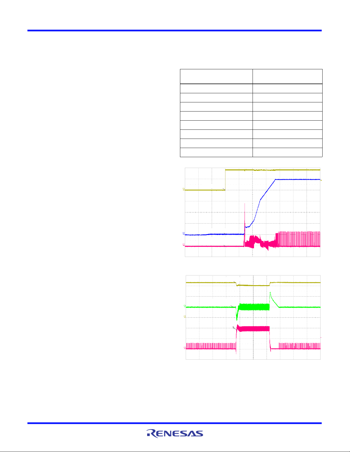
the expected waveforms are shown in Figures 2 and 3.
Quick Setup Guide
1. Install jumper on J3, shorting EN to VIN.
2. Install jumper on J4, shorting MODE to VIN.
3. Connect power supply to J1, with voltage setting between
1.8V and 4.8V.
4. Connect electronic load to J2.
5. Place scope probes on the VOUT test point, and other test
points of interest.
6. Turn on the power supply.
7. Monitor the output voltage start-up sequence on the scope.
The waveforms will look similar to that shown in Figure 2.
8. Turn on the electronic load.
9. Measure the output voltage with the voltmeter. The voltage
should regulate within datasheet spec limits.
10. To determine efficiency, measure input and output voltages
at the Kelvin sense test points (S+ and S-), which are part of
J1 and J2 headers. The bench power supply can be connected
to the PVIN and GND headers on J1. The electronic load can
be connected to the VOUT and GND headers on J2. Measure
the input and output currents. Calculate efficiency based on
these measurements.
11. To test external sync, remove the jumper at J4, then apply an
external clock between 2.75MHz and 3.25MHz on the MODE
input (the center pin of header J4).
12. Set the electronic load to constant current dynamic mode
with 10mA to 1A pulse, tON= 500µs. Check the load transient
response as shown in Figure 3.
TABLE 1. OUTPUT VOLTAGE PROGRAMMING For ISL91117IIA-EVZ
DESIRED OUTPUT VOLTAGE
(V)
R1 RESISTOR VALUES
(k)
2.0 90.9
2.5 127
3.0 165
3.3 187
3.6 210
4.0 243
4.5 280
5.0 316
EN (2V/DIV)
VOUT (1V/DIV)
500µs/DIV
INDUCTOR CURRENT
(500mA/DIV)
FIGURE 2. ISL91117 START-UP WITH VIN = 3.6V and VOUT = 5V
VIN (1V/DIV)
INDUCTOR
CURRENT (1A/DIV)
VOUT, 5V OFFSET
(200mV/DIV)
200µs/DIV
10mA – 1A
LOAD TRANSIENT
(240mA/µs SLEW
RATE)
FIGURE 3. ISL91117 LOAD TRANSIENT AT VIN = 3V AND VOUT = 5V


