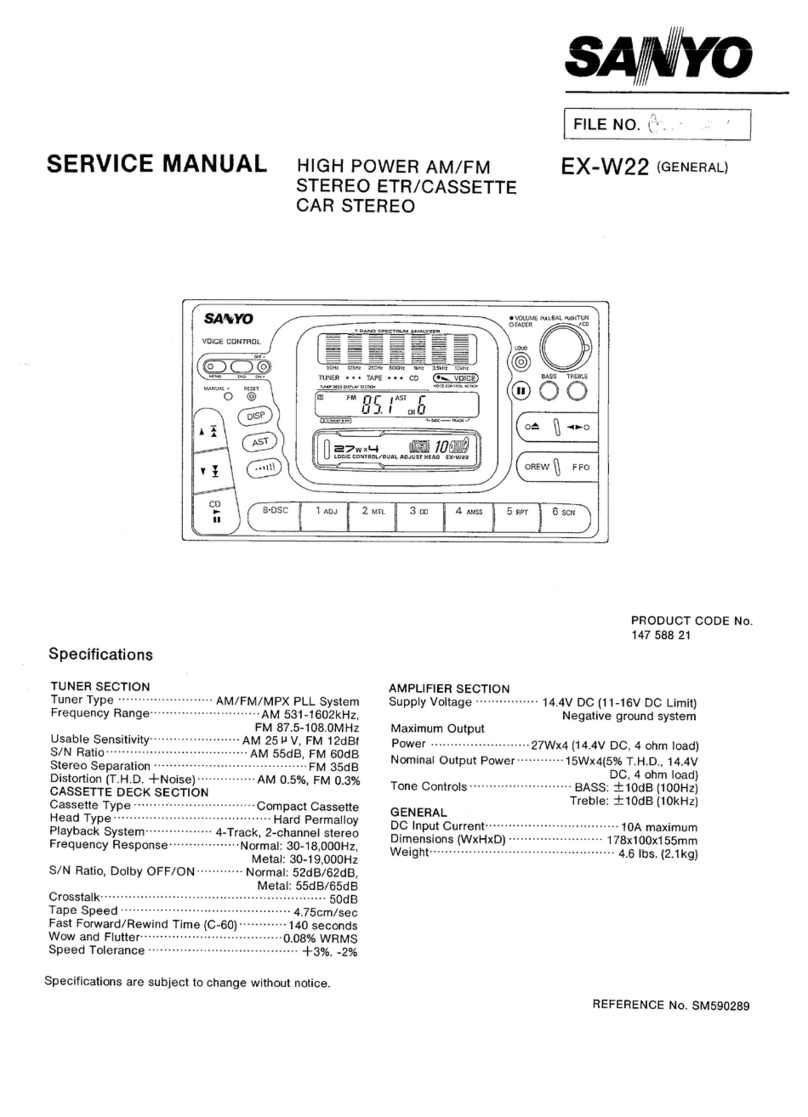
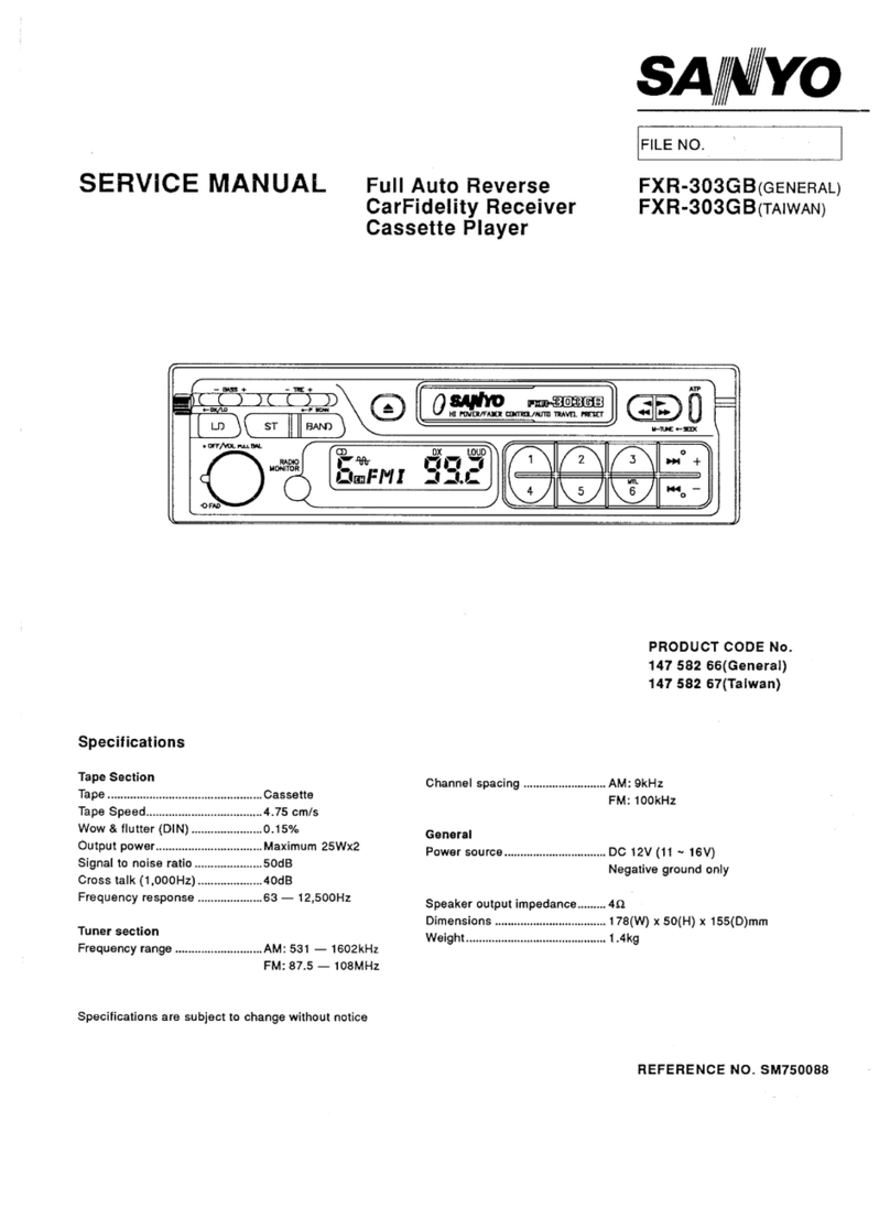
Sanyo CDF-R800 User manual

L
SERVICE MANUAL Multi Control
CD Receiver
i
S*O
I
—
wm—m ——
FILE NO.
CDF-R800(GENERAL)
PRODUCT CODE No.
14759079
Specifications
COMPACT DISC
Disc ................................................ Compact Disc
Laser diode properties ........... Material :GaAIAs
Wavelength :790nm
Spindle speed ..”””..””200 r.p.m to 500 r.p.m(CLV)
Error Correction ........... Cross interleave Reed
Solomon Code
Number of channels ........................................... 2
D-A Conversion ................................... 16 bit twin
Frequency response ..o.......oS””OOO.OS””O5-20,000 Hz
Harmonic distortion ..................s..””’0.03Yo(1 KHz)
Dynamic range ............................................. 85dB
Signal to noise ratio ..................................... 90dB
Channel separation ......................... 70dB (1 KHz)
Wow and Flutter ............ Below measurable limit
Specifications are subject to change without notice.
L
FM TUNER SECTION
Frequency Range ........................... 87.5-1 08MHz
Sensitivity ..................................................... 12dB
Signal to noise ratio ..................................... 60dB
Stereo separation ......................................... 35dB
AM TUNER SECTION
Frequency Range ............................ 522-1 620KHz
Sensitivity ..................................................... 28dB
Signal to noise ratio ..................................... 50dB
GENERAL
DC power supply..”””””””””””””-””DC14.4V (llV-16V)
Maximum output power .......................... 30W x 4
Continous power output o..000”-Q.”.o”oo”o”o.oo”o15W x 4
Current Drain .................................................... 8A
Tone Action (BASS) ................... *l OdB(100kHz)
(TREBLE) .................. *lOdB(lOkHz)
Installation Size (W xHxD). 178x50x 158 mm
REFERENCE No. SM590452

DISASSEMBLY
TOP CHASSIS
I
MAIN PCB d
1.Push up the rear right part of the top chassis.
Then the top chassis will come off.
PANEL ASSY
1.Unhookthe Panel’s stoppers located on both the left and
right sides and the center bottom.Then the panel assy will
come off.
CD MECHANISM
1.Remove4screws@ fixing the mechanism in the chassis.
Disconnect the main PCB’S FPC from the mechanism’s
soket,Then the mechanism will come off.
1.Remove 3screws@) and 2 screws ~securing the heat
sink.
2.Remove the Base and Special screw.
3.Remove 2screws @) and 1 screw@ fixing the front
chassis to the chassis.
4. Remove 1screw@ securing the IC -bracket.
5.Remove the solder on the wire which connects the main
PCB and the chassis.Then the main PCB will come off.
“d
HANISM
A
‘e’
–l–

DISASSEMBLY
LCD MECHANISM
A. How to remove pick up.
1. Make the FPC’Sshort-round short-circuit.(A-l )
2. Remove ascrew ~fixin pick up. (A-1)
d
3. Pickup (@ and shuft E12 will come off.(A-l )
Q
E6
,
L.
I
—-.-- .---—-------------------------
o10$(
B. How to remove feed motor.
1. Remove 4screws ~Fixing damper. (A-2)
2. Remove 3springs ~and a spring ~
3. Pull magnetic coil mto rotate gear ~.
Continue it until microswitch ~turns on.
Then move CD unit to gear -side and pull it up to
A– 1remove it.(A-2)
4. Remove ascrew @fixing the motor.(A-3)
5. Motor @and fixture ~will come off.(A-3)
6105 A–2 oIo5
.(A-2)
–2–

DISASSEMBLY
C. How to remove spindle motor.
1. Remove 4fixtures ~.(A-3)
2. Remove 2special screws @.Then clamp fixture
assy (R) @will come off. (A-4)
3. Remove atorsion spring ~.
Then clamp chassis assy @will come off.(A-4)
4. Remove 2screws @fixing motor assy ~.
Then motor assy @J will come off.(A-5)
9
E103
1! Id
A–3
@@m
-f-Y ---
11 n‘-----------2---------N
/1<
A–4 A–5
–3–

DISASSEMBLY
LD. How to remove loading motor.
1. Remove atorsion spring ~.(A-7)
2. Remove aguide ~-.(A-7)
3. Remove aspecial washer ~.(A-7)
4. Remove atorsion spring @.(A-8)
5. Remove special washers (~ and ~).
Then plate @will come off. (A-8)
6. Remove gear @.(A-8)
7. Remove special washers (@@ and @).(A-8)
8. Remove gears (~and =)and roller.(A-8)
9. Remove aguide @.
Then roller bracket will come off.(A-8)
10. Remove ascrew@ .(A-8) o
E06_A7
L’
11.
12.
Remove 2screws@ .(A-8) Then motor fixture
assy @will come off.(A-9)
Remove 2screws ~.
Loding motor will come off.(A-9)
A-9
–4–

NOTES REGARDING COMPACT DISC PLAYER REPAIRS
(1) Preparations
1)Compact disc players incorporate agreat many ICS as well
as the pickup (laser diode). These components are
sensitive to ,and easily affected by ,static electricity. If
such static electricity is high voltage, components can be
damaged, and for that reason components should be
handled with care.
2) The pickup is composed of many optical components and
other high-precision components. Care must be taken,
therefore, to avoid repair or storage where the temperature
of humidity is high, where strong magnetism is present, or
where there is excessive dust.
(2)Notes for repair
1) Before replacing acomponent part, first disconnect the
power supply lead wire from the unit.
2) AH equipment, measuring instruments and tools must be
grounded.
3) The workbench should be covered with aconductive sheet
and grounded.
When removing the laser pickup from its conductive bag,
do not place the pickup on the bag. (This is because there
is the possibility of damage by static electricity.)
4) To prevent AC leakage, the metal part of the soldering iron
should be grounded.
5) In removing short circuit solder of LASER PICKUP, use
ceramic heater type of soldering iron.
6) Workers should be grounded by aearth band (1MQ).
7) Care should be taken not to permit the laser pickup to
come in contact with clothing, in order to prevent static
electricity changes in the clothing to escape from the
earth band.
8) The laser bea mfrOm the Dicku~ should NEVER be
directly facing the eves orbares kin.
Countermeasure of electrostatic
Resistor A
(lMCr) ~
NOTES REGARDING HANDLING OF THE PICKUP
(1) Notes for transport and storage
1)
2)
3)
In retaining the product, high temperature, high humidity
and dusty circumstances must be avoided. After taking it
out of packing box, never leave it at the place where dust
can occur. (Take every possible preventive means
against dust. )
The pickup should always be left in its conductive bag
until immediately prior to use.
As this is minutely adjusted, be careful never give it any
shock from drop or careless handling.
Storage in conductive bag Drop impact
(2) Repair notes
1)The pickup incorporates astrong magnet, and so should
never be brought close to magnetic materials.
–5–

1
1
L
L.
L
NOTES REGARDING HANDLING OF THE
2) The pickup should always be handled correctly and
carefully, taking care to avoid external pressuer and
impact. If it is subjected to strong pressure or impact, the
result may be an operational malfunction and/or damage
to the printed circuit boaed.
\
How to hold the pickup
Grabbina Drint circuit boa rd or DUIling
co nnectina wire causes function
deterioration or failure. Be sure to hold
the whole hous ins.
3) If LASER PICKUP or MECHA ASSY is set or reset with
power supplied. LASER DIODE or PHOTO DETECTOR
is damaged. Be sure to turn off power supply switch
before setting or resetting LASER PICKUP or MECHA
ASSY.
4) To prevent LASER DIODE or PHOTO DETECTOR from
being deteriorated or damaged by static electricity, be
sure to thoroughly practice earthing as apreventive
means against damage from static electricity.
5) Take every possible means against damage of LASER
DIODE or PHOTO DETECTOR from overcurrent or
overvoltage. (Example--Use power source equipped with
current limiter. )
6) If fingerprint or any other foreign material is attached on
objective lens, the function is extremely deteriorated. Be
sure never to touch objective lens. Particularly, be very
careful in removing or fitting lens cover.
PICKUP
7) PICKUP is asingle part, and very minutely adjusted as
such. Therefore, never touch anv of adjustment DO
fixina screws or Drint circuit bints.
oard of PICKUP.
(1) If you touch partially fixed volume soldered on circuit
board (beam quantity adjusting volume), emitted
beam quantity (RF LEVEL) can change. Never touch
partially fixed volume.
(2) If there occurs even avery small shift in the circuit
board fixture position, the function greatly changes. In
handling LASER PICKUP, be very careful to hold
metal part of housing (HOUSING).
8) If metal part of adjusting rod or driver touches circuit
board when power is supplied, it can cause failure. Be
careful.
9) Laser beam may damage the eyes!
Absolutely never permit laser beams to enter the eyes!
Also NEVER switch ON the power to the laser output
part (lens, etc.) of the pickup if it is damaged.
LaserBeam
~+
NEVER look directly at the
laser beam, and don’t let
contact fingers or other
exposed skin.
o
1o)
11)
Cleaning the lens surface
If there is dust on the lens surface, the dust should be
cleaned away by using an air brush (such as used for
camera lens). The lens is held by adelicate spring.
Never attempt to disassemble the pickup.
–6–
NOTES REGARDING HANDLING OF THE PICKUP
Touching this part can cause function
deterioration. Pleasde be careful never to
touch this part.
It
P#ially
. .
&
Holding and pulling flexible wire can cause
breaking of wire. Please be sure to hold the
PICKUP DEGITAL
PD
VR
GND
LD
Vcc
Vc
3F
AIL
T-
RACK-
4G T+
F-
ocus F+
CONNECTOR
PIN ITERMINAL] SYMBOL
E#=l
1PDIC PD2
2PDIC PD1
3PDIC E
4LD PD
5LD VR
6PDIC/LD GND
171 LtIl LDl
1121 PDICI A/L I
--
–7–

1
I
L
WIRING
General 1Antennaso
DINAntyma
+J CD ChangerDIN ~I
Socket(Seapege8.)
fi( ,,
111111II (GND) @2Groundwire(Black)
111111II .,
(ACC) ~3+12VAccesso@gnitionwire(Rad)
111111~(B. UP) =4 +12V Constant Dower suodv wire(Yellow)
1111/ ,,, . ,
(P.ANT)D5power antenna control wire(Blue)
&
---- 4-Spaaker system ---.,
IFL+(WWie) ee
3
Front Letl ~
IFL-(whir*@ e e Speaker :
I!Ei
‘FR+(Grny) @e ,
‘FR-(Gray~lesk) 3
Front Right f
eSpeaker I
aRL+ Green @,
a
Rear Left ~
1RL<GrewShck) Speaker [
/---- 2-Spaaker system ,
-----
,FL+(wm) ,
,
t@e
!- “..-... ,,.. I
rrorn tog
I
,RL-(Gr&Q Iack) eo
‘-------------------------- J‘___________________________ .’
When connecting aCD Changer
Connect the end of DIN cable (8 pin), which is supplied with the SANYO CD Changer, to the CD
Changer DIN socket of CDF-R800, and connect the other end to the CD Changer.
Note:
The ID Switch of CD changer should be set to ‘7” position
CDF-R800
DIN
When Connecting two CD Changers
Aseparately available SANYO Divider unit (FTP-CH1S) is necessary to connect two CD
Changers. As to the details, follow the manual of Divider unit.
Note:
Set the ID Switches of CD changers to”1” or “2” position respectively.
CDF-R800
l-’
~@ See page 8.
DIN Antenna plug II
DIN Cable(8pin) DIN”Cable(8pin)
–8–

:
CIRCUIT OPERATION DESCRIPTION
LC72338-9330
PIN
1DESCRIPTION
4.5MH2 Crystal oscilator connection
LSI TEST2 Terminal(GND)
TERMINAL NAME
XIN
TEST2
2
3SUB-Q data Terminal ‘
Command output Terminal
Serial clock output Terminal
SUB-Q Sianal inrxrt
SQOUT
COIN
CQCK
WRQ
4
5
6
7
8
9
10
0IPC3 Loading M-otor Control output
LM+
LM-
PLANGER
KS4 Planger output
Key return output
PB3
PB2
PB1
11
12
13
14
15
16
17
18
19
20
21
22
23
24
25
26
27
28
29
30
31
KS3
KS2
KSI
KSO
D3
D2
D1
DO
Key return input
PA2
PAI Iu’
*
LOADING F.
RWC
BUSIN
DRF
Loading Finish(Clamp)input
Data output Latch Terminal
CD charmer control BUS irmut for interrurX function
IIPKO/lNTO Focus lock signal input
Output Terminal for power AMP control
FEED MOTOR control output (outside)
FEED MOTOR control output (inside)
LO/DX Select output Terminal
DISC loading start,8cmDlSC loading completion Detect Signal input
12cmDlSC loading completion Signal input
12cmDlSC Eject completion Signal input
pOWER ANT COntrOiOUtDUt
STBY
FEM+
FEM-
LO/DX
SENSOR A
SENSOR B
SENSOR C
PANT
oS291PM0
=+==
IS281PM3
IS271PM2
IS261PM1
oS251PM0
–1 VDD VDD
SENSOR DVDD
32
33
34
35
36
37
38
39
40
I
55
56
57
58
59
60
61
62
63
64
IIPF3/Sl 1DISC loading completion Detect Signal input
VR control data output
VR control clock outcwt
IQPF2/SOl
oPF1/SCKl
oPFOIS21
oS201PE31S
VR DO
VR CL
VR CE VR chiD enable control outmrt
S20
S19
S18
S17
S16
I
LCD Driver segment output
S191PE21S
s18/PEl/s
S171PE0
S16
I
S1
COM3
COM2
S1
COM3
oLCD Driver common output
COM2
a=
COMI
—VDD2
—VDD1
oPJ31DAC3
oPJ21DAC2
oPJ1/DACl
oPJOIDACO
IPH31AD13
IPH2/AD12
COM1
VDD2
VDD1
MUTE
CD+B
VDD2 for LCD
VDD1 for LCD
Audio Mute output
VDD for CD Block
FM+B FM Band Select outDut
BUSOUT
INSIDE Changer control Bus
Pickup innermost position detect Terminal
Temperature Abnormality Detect Terminal
Radio stereo Broadcast Sianal incmt
65
66
67
68
TEMP
STIN
S*M Field strength Signal input
–9–

DESCRIPTION
L
—
L
PIN 1/0 PORT NAME TERMINAL NAME DESCRIPTION
69 IHOLD CE Chip enable Detect input
70 IHCTR IFIN FM .AM IF Signal input
71 ILCTR SDIN Station detect input
72 ISNS SNS SENSE Signal input Terminal
73 – VDD VDD VDD
74 IFMIN FMVCO FM VCO
75 IAMIN AMVCO AM VCO
76 – Vss GND GND
77 0 EO1 EO1 Charge pomp output (Error out signal)
78 E02 E02
79 – TEST1 TEST1 LSI Testl Terminal (GND)
80 0 XOUT XOUT Crvstal oscilator connection
LC78622E
PIN PORT 1/0 DESCRIPTION
NAME
1 1 ,
1DEFI I I IDefect detect sianal (DEF) inrmt terminal.
2TAI
3PDO
4Wss
5ISET
6WDD
7FR
8Vss
9EFMO
10 EFMIN
11 TEST2
12 CLV+
13 CLV-
14 VIP
+=
15 HFL
16 TES
17 TOFF
18 TGL
19 JP+
-.7 .
IPLL Input terminal for testing .Pulldown resistance is self-containce.
oPhase comparison output trminal for outer VCO control.
Power supply terminal for self-contained VCO. Normally OV.
Al Resistance connecting terminal for PDO output current adjustment.
Earthing trminal for self-contained VCO. Normally 5V.
Al For VCO range frequency adjustment.
Earthing terminal for digital system. Normally OV.
oFor slice EFM signal reverse output terminal.
Ilevel control EFM signal input terminal.
IInput terminal for tesying. Pulidown resistance is self-contained.
oOutput terminal for spindle servo control. Accelerates when CLV+ is “H”,
oslows down when CLV- “H”.
oOutput trminal for automatic switchover monitor by rough servolphase control.
“H’’causes rough servo “L’’phases control mode.
IInput terminal for track detecting signal. Schmidt input.
IlnDut terminal for tracking error signal. Schmidt input.
oOutput terminal for track~g OFF. -
0Output terminal for tracking gain switchover, “L” raises, gain.
oOutput terminal for track jump.When JP+ is “H”, accelerates at the time of
20 JP- Io outer track direction jump, or”slows down at the time of inner track direction
jump. When JP- is “H”, accelerates at the time of inner track direction jump,or
slows down at the time of outer track direction. 3value output is possible by
command.
21 PCK oClock monitoring terminal for EFM data playback. At the time of phase lock,
4.321 8MHz.
22 FSEQ oOutput terminal for synchronous signal detection. When synchronous signal
detected from EFMsignal and synchronous signal occurring inside correspond,’’H”.
23 VDD -Earting terminal for digital system.
24 CONT1 1/0
+=
25 CONT2
26 CONT3
27 CONT4 4
1/0 Input /output terminal.
1/0
28 ICONT5 11/0
=lo–

CIRCUIT OPERATION DESCRIPTION
-1-
PIN PORT
NAME
29 EMPH
1/0
o
DESCRIPTION
Output terminal for reemphasis monitor.
At the time of “H”, reemphasis disc is in playback.
30 C2F oC2 Frag output.
31 DOUT oDigital Out output terminal.
32 TEST3 IInput terminal for testing. Pulldown resistance is self- contained.
33 TEST4 IInput terminal for testinq. Pulldown resistance is self-contained.
/
--
H=
35 MUTEL
36 LVDD
37 LCHO
I38 ILVSS
R--w
41 RVDD
42 MUTER
43 XVDD
44 XOUT
45 XIN
46 Xvss
47 SBSY
48 EFLG
49 Pw
50 SFSY
El=
H=
53 WRQ
54 RWC
55 SQOUT
56 COIN
57 CQCK
H=
58 RES
59 TST11
60 16M
oFir 1bit DAC Mute output terminal.
Power supply terminal for Lchannel.
oLchannel Ooutput terminal.
Earting terminal for Lchannel. Normally OV.
Earting terminal for Rchannel. Normally OV.
oRchannel Ooutput terminal.
Earting terminal for Rchannel. Normally OV.
oMute output terminal.
Power supply terminal for crystal oscillation. Normally 5V.
oConnecting terminal for 16.9344MHz crystal oscillator.
I
I
-i5-
Earthing terminal for crystal oscillation. Normally OV.
Output terminal for synchronous signal of sub-code block.
Terminal for monitoring Cl ,C2, single, double correction.
Outtwt terminal for sub-code P.Q.R.S.T.U.W.
Ou~put terminal for synchronous signal of sub-code frame.
When sub-code is in standby, “= L”.
Input terminal for sub-code readout clock. Schmidt input.
Output terminal for 7.35kHz synchronous signal which is divided frequency from
crystal oscillation.
Output terminal for sub-code Qoutput stabdby.
Input terminal for read/write control.
Sub-code Qoutput terminal.
Input terminal for command from micro computer.
Input terminal for command input intake clock,or sub-code offtake clock from
SQOUT. Schmidt irmut. I
Chip reset input terminal. When power is supplied, changeover to “L” once.
Input terminal for testing. Open (Normally “L” output).
16,9344MHz output terminal. But outputs 33.8688MHz, only in case of quadruple
speed playback mode.
61 4.2M o4.2336 MHz outDut terminal.
-
b62 TEST5 IInput terminal for testing. Pulldown resistance is self-contained.
63 Cs IChip select input terminal. Pulldown resistance is self-contained.
64 TEST1 IInput terminal for testing. Pulldown resistance is self-contained.
–11–

‘“%.-
L
L
CIRCUIT OPERATION DESCRIPTION
LA9240MS #
PIN PORT NAME DESCRIPTION
1FIN2 Pickup photo-diode connecting pin. Forms RF signal by addition to FIN1 pin,and FE signal by
subtraction.
2FINI Pickup photo-diode connecting pin.
3EPickup photo-diode connecting Din. Forms TE sianal bv subtraction from FDin.
4FPickup photo-diode connecting pin.
5TB Pin for inputting DC constituent of TE signal.
6TE- Pin for connecting gain setting resistance of TE sianal to TE Din.
7TE TE signal output pin.
8TESI TES(TRACK ERROR SENCE) comparator input pin. Band pass TE signal, and input.
9Scl Input pin for shock detection.
10 TH Constant setting pin at the time of tracking gain. of servo.
11
I12 TD- 1Pin for constituting; tr~ckina Dhase compensation constant between TD and VR Din.
11 TA IPin for connect~a hiah ~ass elimination condensor
~.
13 TD Pin for setting tracking ph;se compensation.
14 JP Pin for setting tracking jump signal (kick pulse) amplitude.
15 TO Tracking control signal output pin.
16 FD Focusing control signal output pin.
17 FD- Pin for constituting focussing phase compensation constant between FD and FA pin.
18 FA Pin for constituting facussing phase compensation constant between FA- and FE- pin.
19 FA- Pin for constituting focussing phase compensation constant between FA and FE pin.
20 FE FE signal output pin.
21 FE- Pin for connecting FE signal gain setting resistance to TE pin.
22 AGND GND for analog signal.
23 SP Signal end output of CV+ and CV- pin input signal.
24 SPI Spindle amplifier input.
25 SPG Connecting pin for gain setting resistance at the time of spindle 12cm mode.
26 sP- Connecting pin for spindle phase compensation constant together with SPD pin.
27 SPD Spindle control signal output pin.
28 SLEQ Connecting pin for sled phase compensation constant.
29 SLD Sled control signal output pin.
30 SL- Input pin for sled delivery signal from micro computer.
31 SL+ Input pin for sled delivery signal from micro computer.
32 JP- lnDut Din for trackina iumD signal from DSP.
33 JO+ Input pin for trackin~ ~umpsi~nal from DSP.
34 TGL Input pin for tracking gain control signal from DSP.Gain low in case of TGL=’’H”.
IIfrom DSP.Off in case of TOFF=’’H”.
35 TOFF Input pin for tracking Gff control signs
36 TES Output pin of TES signal to DSP.
37 HFL (HIGH FREQENCY LEVEL) is used to judge whether main beam is located
above pit or above mirror.
38 SLOF Sled servo off control input pin.
39 cv- Input pin for CLV error signal from DSP.
40 Cv+ Input pin for CLV error signal from DSP.
41 RFSM RF output pin.
42 RFS- Pin for setting RF gain and EFM signal 3T compensation constant together with RFSM pin.
43 SLC (SLICE LEVEL CONTROL) is output pin for controlling data slice level by RF waveshape DSP.
44 SLI Int)ut Dinfor controlling data slice level bv I?@D
,––-,– J-r .
45 GND pin digital syste;. .
DGND
46 FSC For Foes Smoosing capacita output pin.
ZrT TBC [Tracking Balance control pin.
INO CONNECT.
andard clock input pin. DSP 4.231
51 CL IMicro computer command clock input pin.
48 NC
49 DEF Output pin for detecting disc defect.
50 CLK St: IMHZis input.
52 DAT put pin.
1
53 CE IMic ‘
rIMicro commter command data in
:ro computer command chip enable input pin.
t 541 DRF I[DEFECT RF) RF level detecting output.
–12–

CIRCUIT OPERATION DESCRIPTION
PIN PORT NAME DESCRIPTION
55 FSS Foca serch select pin.
56 VCC2 VCC pin for servo system and digital system.
57 REF1 Connection pin for standard voltage capacitor.
58 VR Standard voltage output pin.
59 LF2 Pin for setting constant at the time of detecting disc defect.
60 PHI Pin for connecting condensor for RF signal peak hold.
61 BH1 Pin for connecting condensor for RF signal bottom hold.
62 LDD APC circuit outwt Din.
63 LDS APC circuit input pin.
64 Vccl RF system VCC pin.
IC BLOCK DIAGRAM
IN1
GND
LB1641
PI OUT1VCC20UT2 P2 VCC1
--@ @@@@@-
MC14069UBF
1
{’ INPUT L-j
I
(y I
w
12
34
)Vz 56
m
S-80732AN
VDD
Vss
!!3
11 10
13 12
Vss 714 VDD
_.
d
–13–

Ic BLOCK DIAGRAM
L
AI
L
i
XIN
XOUT
FMIN
AMIN
SNs
VOD
Vss
HCTR
LCTR
HOLD
PAO
PAI
PAZ
PA2
PBO
PSI
PB2
PB3
Pm
Pcl
PC2
PC3
PGo
TSET1
TEST2
EO
E21s02
FO
sCKW
soolPG2
sloiPG3
I,,l,Q=
SD
I
I
I
LATCH
c%%.
m
RCtA
sKX1=
+NsTml-
C?WN
-1!
?
AODRESS OECOOER
lT
IPFU5RU4 CCUJTER I
11
ISTACK 1I
I~S20FEWS12
s2sFPa
-1
s27/PM2
S2snws
S29/PN08EEP
s20fw41
B211QN2
S2ZJPNS
&!lli=+”mpJ”AcO
=lI!i%
u,Nm,
AOC MPX
IATCH
M,.
1I
L
–14–

IC BLOCK DIAGRAM
LC78622
DEFI VCO CLOCK mxsut
d
oscHJXrloN t
CLCCK
cONTRC4 RAM GENERATOR
I
IJII 1
+’-A
SYNO
DETECTION /(
EFM
DEMODUIATIDN MUTE
,
$C2F
)DOUT
]NC
FSEQ
CLV+
CLV–
VP
Pw
SBCK
SSSY
SFSY
Cs
WRQ
km-h CIC2 ERROR
DETECTICN
CORRECTION
FI Ae r
tiDIGITAL
CUT
P
DIGITAL
AITENLIATOR
YI--- .—
11111 I----
PROCESSING I
Ill I I
K==w--lrr -i 4TAIMES OVER SAMPLING
DIGITAL FILTER
P1 (
lMt DAC —
INVCC PVCC2
STSY
IN1
IN2
IN3
IN4
MUTE
L
!
I
--
$=!
7
Q
AMP2 8
e9
INPUT BUFFER 2I
AMP3
AMP4
4INPUT BUFFER 4\
L&&r_
w
–15–

Ic
L.. LA9240MS BA3121F
—
+
FIN I2
[
E3
F4
T6$I
TE- 6
TE 7
TESI 6
3CH 9
TH
I
TA II
Tel- 12
In
—
Ja=
F?’
OAL VCA
=-i-
T.SERVO8T. LOGIC
1
Ea-
n
JINC
NC
NC
&ffitJo
8
+- SLl
SLC SLc
RPS-
Rp ●-
MP IRFSM
-s$w+
Cv-
_c$-
HFL
.,.
Vml Vm2
IN 2
0UT2
GND
1+-I
1II
t11
---TTJ-L
–16–
EXPLODED VIEW
–17–

L
L
L
PARTS LIST
Ref. No. PART No. DESCRIPTION
INDIVIDUAL
~A(
T6322961661
6326564059
6327985242
6326096844
6326044757
4110316006
CESSORY
POLYETHYLENE BAG
ASSY,CASE
CORD,AT7ACHMENT
POLY COVER, I30X25CI
LEVER,HOOK
SCR BIN 3X20
SHIPPING
6326229934 NOTICE
SHIPPING
6325449265 TRIM PANEL
6322961706 POLYHHYLENE BAG
CABINET
16328069637 ASSY,PANEL
2 6326069644 ASSY,PANEL
3 6327964209 SHEET,A,POWER
4
5
6
7
B
6327964216
6327964223
6327964230
6327964247
6326006564
SHEET, B,ATP,LOUD
SHEET, C,SEL
SHEET, D,DISP
SHEET, E,CHG
SHEET, F,SEEK
9
10
24
25
11
12
30
13
28
29
14
15
16
16
17
17
18
19
CHASSIS
6328013920 ASSY,CHASSIS
6326001712 ASSY,CHASSIS,TOP
6326044764 BRACKET-M,SE7
BRACKET-M, SET,R
6326083954
4110328504
4110285906
4110262905
4110285906
6326061622
4110265906
4111200700
4110282905
6328009565
6325683034
6327916222
6325506535
6326004171
6327175827
6327691839
6322834927
6325462943
6327916130
6327916147
6327916161
6327916154
6327916178
6327996101
SCR BIN 5X6
SCR S-TPG PAN 2.6X5
F.CHASSIS -CHASSIS
SCR S-TPG PAN 2X4
F,CHASSIS -CHASSIS
SCR S-TPG PAN 2.6X5
MECHANISM
HEAT SINK
SCR S-TPG PAN 2.6X5
HEAT SINK -CHASSIS
SCR S-TPG BIN 2.6X6,1C
SCR S-TPG PAN 2X4
BRACKET IC
CUSHION,SW
CUSHION
INSULATOR
LABEL, IDENTIFICATION,CLAS
LABEL, FUSE,1OA
LABEL, IDENTIFICATION
LABEL,CAUTION, LASER
SPECIAL SCREW
BASE
CHASSIS, FRONT
SHEET, LCD
MOUNT-E, LCD
tHOLDER
BRACKET-E, LCD
BRACKET
BRACKET-E,IC
LUMINANT
1
1
1
1
2
1
1
1
1
1
1
1
2
1
1
1
1
1
1
1
1
2
2
1
4
1
3
2
1
2
1
1
1
1
1
1
1
1
1
1
1
1
1
1
—
CHASSIS ELECTRICAL
6328022373 CD MECHANISM, M90212 1
NO SERVICE PART
?0 6326068739 TUNER,AWFM 1
Ref. No. PART No. DESCRIPTION Qty
21 6327960667 LCD 1
MAIN P.C.B. ASSEMBLY
PCB1 6328068027 ASSY,PCB-W,MAIN 1
ANT 6322517349 SOCKET, ANTENNA 1
JK201 6325197096 PLUG, 6P 1
cP5ca 6326564721 SOCKET, I6P 1
L301 6322650305 CHOKE COIL, 27UH 1
X801 6326490174 RESONATOR,XTAL,4 .5MHZ 1
PL501 6326004928 LAMP,5V,11 5MA 1
PL502 6326004928 LAMP,5V,I 15MA 1
F501 4230264201 FUSE 125V IOA 1
FPC901 6326014927 WIRE,26P-200MM 1
IC601 4094046203 IC LC72336-9330 1
Iclol 4093735504 IC LC75372E 1
IC201 4092624205 IC BA3121 F1
IC401 4093966302 Ic HA13157 1
D509 4070040607 DIODE DCBOIO 1
D501 4071903703 DIODE RB050L-40 1
D51O,511 4070058602 DIODE ERA15-02 2
D301 ,302, 4070764204 DIODE MA165 7
D502,303,
D304,305
D306
D512 4070694909 DIODE DSBO1O 1
D201 4071006008 ZENER DIODE HZS5BLL 1
D602 4070636606 ZENER DIODE MTZJ5.lA
D504,505 4070636903 ZENER DIODE MTZJ5.6C :
D503 4070996102 ZENER DIODE MTZJIOB 1
D506,507 4070639702 ZENER DIODE MTZJ9.lC 2
D506 4070636309 ZENER DIODE MTZJ1 lC
Q501 ,502, 4051242402 TR 2SB1424-R I:
Q506
Q501 ,502, 4051242303 TR 2SB1424-Q ‘R 3
Q506
Q507 4051426606 TR 2SD2576-F 1
Q512,513, 4050294501 TR 2SD1658-R 3
Q514
Q51 O4050293504 TR DTCI 44EK 1
Q5433,504, 4050003606 TR DTCI 14YK 3
Q406
Q301 ,505 4050293207 TRDTC114TK 2
Q601 4050293009 TR DTA1 14YK 1
Q302,306 405093 9s06 TR 2SAI 179R-M6 2
Q303,304, 4050156704 TR2SC2612-L6
Q508,511, 5
Q602
Q303,304, 4051112406 TR 2SD601A-R ‘R
Q508,511, 5
Q602
Q509 4050636305 TR DTB1 13ZK 1
Q307 4050660906 TR 2SK932-23 1
TH501 4080354701 THERMISTOR ZPC13CE1 R5B1 UC 1
KEY 1P.C.B. ASSEMBLY
PCB2 6327961619 ASSY,PCB-W,KEY,I 1
S651 -660 6326569030 SWITCH, TACT,l P-IT Ic
D851 -660 4060317605 LED SLP-7117E-51-TI Ic
CP502 6325400204 PLUG, 4P 1
CP501 6325399645 PLUG, 5P 1
KEY 2P.C.B. ASSEMBLY
PCB3 6327981626 ASSY,PCB-W,KEY,2 1
S861 -869 6326569030 SWITCH,TACT,I P-IT 9
D661 -669 4060317805 LED SLP-7117E-51-TI 9
CP504 6325400204 PLUG, 4P 1
CP503 6325399645 PLUG, 5P 1
COIL P.C.B. ASSEMBLY
PCB4 6328001941 ASSY,PCB-W,COIL 1
L501 6322661073 }
CHOKE COIL OR 1
L501 6322661060 CHOKE COIL 1
NOTES: 1. Part ordars must contain Model Numbar, Part Number and Description.
2. Ordering quantity of screws and resistora must be multiple of 10 PCS.
3. Regular type rasistor and capacitor are omitted. Check the schematic diagram for these values.
–18–

EXPLODED VIEW (CD MECHANISM)
@.
-.
–19–
Other manuals for CDF-R800
2
Table of contents
Other Sanyo Car Receiver manuals

Sanyo
Sanyo FXD-770GD User manual

Sanyo
Sanyo ECD-T1540 Parts list manual

Sanyo
Sanyo T1443 - ECD Radio / CD User manual

Sanyo
Sanyo FXD-680GD User manual

Sanyo
Sanyo ECD-T1137S User manual

Sanyo
Sanyo FXCD-550 - Radio / CD User manual

Sanyo
Sanyo FXD-780RDS User manual

Sanyo
Sanyo FXD-RR1 User manual

Sanyo
Sanyo ECD-T1780DV User manual

Sanyo
Sanyo FXD-MP690R User manual

Sanyo
Sanyo FXR-303GB User manual

Sanyo
Sanyo FXD-770GD User manual

Sanyo
Sanyo EX-600 User manual

Sanyo
Sanyo FXD-MP900 User manual

Sanyo
Sanyo FXD-803LD User manual

Sanyo
Sanyo MAR-B3089 User manual

Sanyo
Sanyo FXR-110GD User manual

Sanyo
Sanyo FXR-100LD User manual

Sanyo
Sanyo FT 200 F-4 User manual

Sanyo
Sanyo FXC-503LD User manual