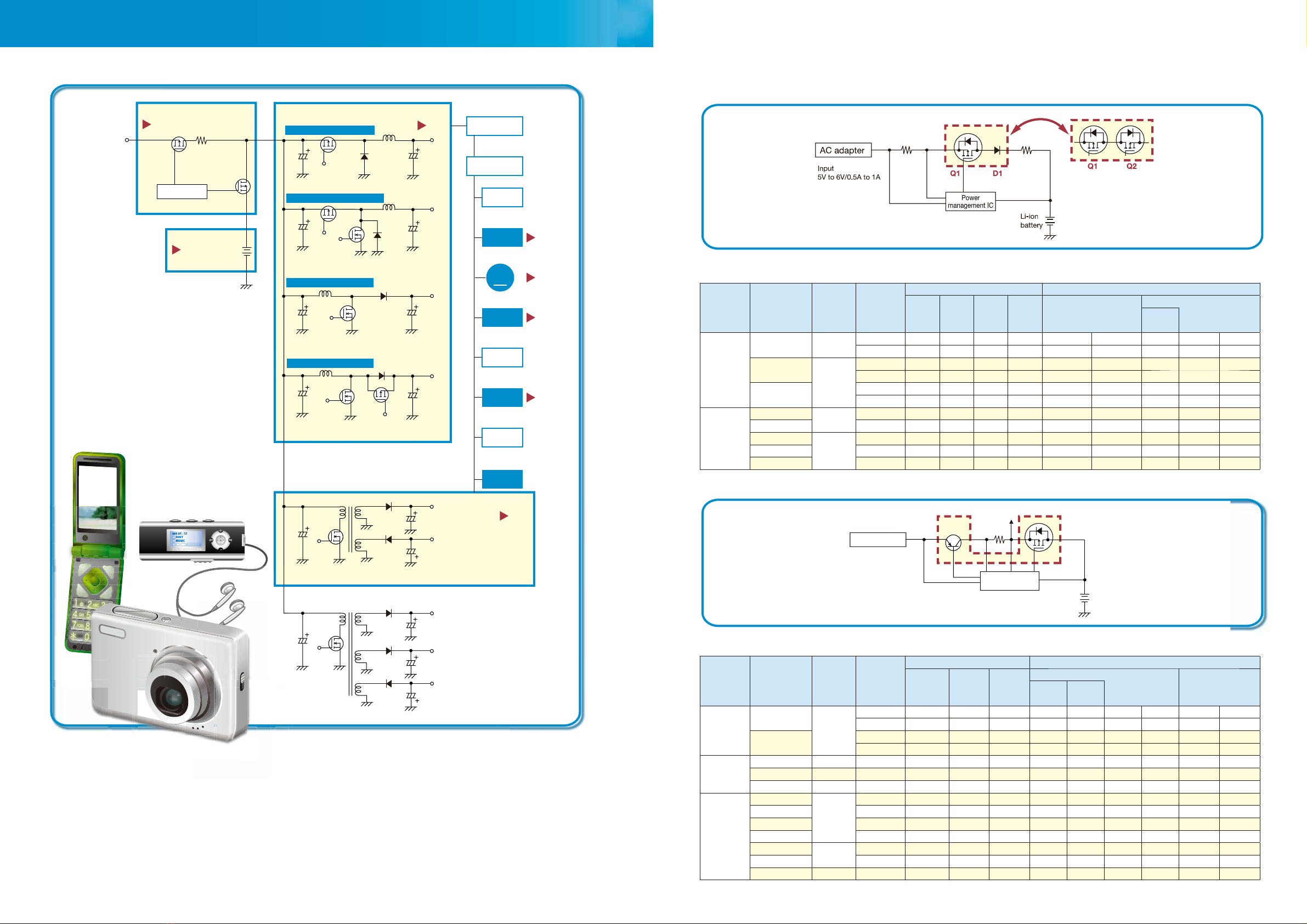
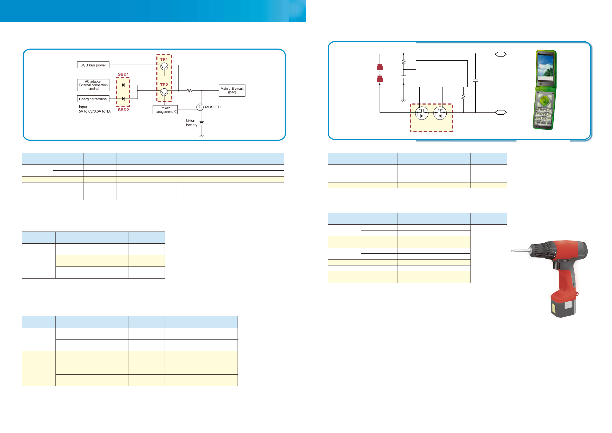
12
Devices for Mobile Equipment
13
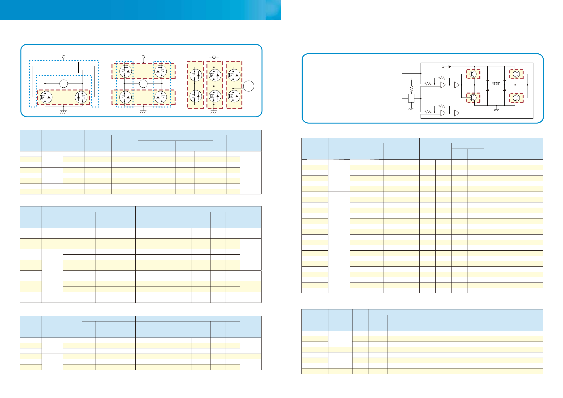
■Devices for Motor
[MOSFETs Use Example]
Single-phase Motor (
H-Bridge, Half pre.
): #5 Single-phase Motor (H-Bridge): #6 Three-phase Motor: #7
M
Q1
Q2 Q4
Q3
Q6
Q5
Q1
Q2 Q4
Q3
Q1 Q2
LB11660V
Motor Driver
M M
MOSFETs (Pch+Nch)
Type No. Package Polarity
Absolute maximum ratings/Ta=25˚C
Electrical characteristics/Ta=25˚C
Use
example
VDSS
[V]
VGSS
[V]
ID
[A]
PD
[W]
RDS (on) [Ω]Ciss
[pF]
Qg
[nC]
VGS=10V VGS=4(4.5)V
typ max typ max
VEC2602 VEC8 Pch 30 20 3 0.9 0.065 0.086 0.117 0.168 510 11 #6
Nch 30 20 4 0.9 0.037 0.048 0.07 0.099 370 8.5
ECH8609 ECH8 Pch 30 20 4 1.3 0.05 0.067 0.087 0.12 550 2.2
#6, #7
Nch 30 20 6 1.3 0.025 0.034 0.052 0.075 510 11
FW340
SOP8
Pch 30 20 5 1.8 0.041 0.053 0.07 0.098 1000 16.5
Nch 30 20 5 1.8 0.037 0.048 0.064 0.09 460 8.6
FW377 Pch 35 20 5 1.8 0.037 0.049 0.062 0.087 1224 24
Nch 35 20 6 1.8 0.025 0.033 0.043 0.061 1050 20
FW356 Pch 60 20 3.5 2 0.11 0.145 0.15 0.21 990 22 #7
Nch 60 20 5 2 0.043 0.058 0.056 0.084 790 16
FW359 Pch 60 20 3 1.8 0.11 0.145 0.145 0.205 990 22 #6
Nch 60 20 3 1.8 0.11 0.145 0.15 0.215 300 7.8
FW360 Pch 100 20 2 1.4 0.24 0.315 0.32 0.45 935 20 #6, #7
Nch 100 20 2 1.4 0.175 0.22 0.22 0.31 530 13
MOSFETs
Type No. Package Polarity
Absolute maximum ratings/Ta=25˚C
Electrical characteristics/Ta=25˚C
Use
example
VDSS
[V]
VGSS
[V]
ID
[A]
PD
[W]
RDS (on) [Ω]Ciss
[pF]
Qg
[nC]
VGS=10(15)V VGS=4(4.5)V
typ max typ max
2SJ646
TP
Pch 30 20 8 15 0.058 0.075 0.097 0.136 510 11 #6, #7
2SJ634 Pch 60 20 8 20 0.105 0.138 0.145 0.205 990 22 #7
2SJ637 Pch 100 20 5 20 0.24 0.312 0.32 0.45 935 20
2SK4067
TP
Nch 30 20 8 10 0.085 0.115 0.155 0.22 260 6 #6, #7
2SK3492 Nch 60 20 8 15 0.115 0.15 0.155 0.22 300 7.8 #7
2SK3617 Nch 100 20 6 15 0.18 0.225 0.225 0.315 530 13
MOSFETs
Type No. Package Polarity
Absolute maximum ratings/Ta=25˚C
Electrical characteristics/Ta=25˚C
Use
example
VDSS
[V]
VGSS
[V]
ID
[A]
PD
[W]
RDS (on) [Ω]Ciss
[pF]
Qg
[nC]
VGS=10(15)V VGS=4(4.5)V
typ max typ max
MCH3410 MCPH3 Nch 30 20 2 0.9 0.115 0.15 0.19 0.27 120 3.6
#5
MCH3421 Nch 100 20 0.8 0.9 0.68 0.89 0.85 1.2 165 4.8
MCH6423 MCPH6 Nch 60 20 2 1.5 0.17 0.22 0.21 0.3 220 6.4
CPH3418
CPH3
Nch 30 20 1.4 0.9 0.23 0.3 0.4 0.56 65 2.5
CPH3424 Nch 60 20 1.8 1 0.17 0.22 0.21 0.3 220 6.4
CPH3427 Nch 100 20 1 1 0.48 0.63 0.58 0.81 240 6.5
VEC2402 VEC8 Nch+Nch 30 20 4 0.9 0.037 0.048 0.07 0.099 370 8.5
CPH6616 CPH6 Nch+Nch 30 20 2.5 0.9 0.079 0.105 0.15 0.21 187 5.2
Devices for Fan Motor
Bipolar Transistors
Type No. Package Polarity
Absolute maximum ratings/Ta=25˚C
Electrical characteristics/Ta=25˚C
Complementary
product
VCEO
[V]
IC
[A]
PC
[W]
hFE VCE (sat) [V]
min max IC
[A]
IB
[mA] typ max
●2SA2124
PCP
PNP 30 2 1.3 *2200 560 1.5 75 0.2 0.4 2SC6044
2SA2012 PNP 30 5 1.3 *3200 560 1.5 30 0.14 0.21 2SC5565
●2SA2125 PNP 50 3 1.3 *3200 560 1 50 0.125 0.23 2SC5964
2SA2013 PNP 50 4 1.3 *3200 560 1 50 0.105 0.18 2SC5566
2SA1416 PNP 100 1 1.3 *3100 400 0.4 40 0.2 0.6 2SC3646
2SA1417 PNP 100 2 1.5 *3100 400 1 100 0.22 0.6 2SC3647
●2SA2126
TP
PNP 50 3 15 *1200 560 1 50 0.135 0.27 -
2SA2039 PNP 50 5 15 *1200 560 1 50 0.115 0.195 2SC5706
2SA2040 PNP 50 8 15 *1200 560 3.5 175 0.23 0.39 2SC5707
●2SA2169 PNP 50 10 20 *1200 560 5 250 0.29 0.58 2SC6017
2SA1592 PNP 100 1 10 *1100 400 0.4 40 0.2 0.6 2SC4134
2SA1593 PNP 100 2 15 *1100 400 1 100 0.22 0.6 2SC4135
2SA1552 PNP 160 1.5 1 100 400 0.5 50 0.2 0.5 2SC4027
●2SC6044
PNP
NPN 30 2 1.3 *2200 560 1.5 75 0.17 0.26 2SA2124
2SC5565 NPN 30 5 1.3 *3200 560 1.5 30 0.125 0.19 2SA2012
●2SC5964 NPN 50 3 1.3 *3200 560 1 50 0.1 0.15 2SA2125
2SC5566 NPN 50 4 1.3 *3200 560 1 50 0.085 0.13 2SA2013
2SC3646 NPN 100 1 1.3 *3100 400 0.4 40 0.1 0.4 2SA1416
2SC3647 NPN 100 2 1.5 *3100 400 1 100 0.13 0.4 2SA1417
2SC5706
TP
NPN 50 5 15 *1200 560 1 50 0.09 0.135 2SA2039
2SC5707 NPN 50 8 15 *1200 560 3.5 175 0.16 0.24 2SA2040
●2SC6017 NPN 50 10 20 *1200 700 5 250 0.18 0.36 2SA2169
2SC4134 NPN 100 1 10 *1100 400 0.4 40 0.1 0.4 2SA1592
2SC4135 NPN 100 2 15 *1100 400 1 100 0.13 0.4 2SA1593
2SC4027 NPN 160 1.5 1 100 400 0.5 50 0.13 0.45 2SA1552
*1: Tc=25˚C *2: When mounted on ceramic substrate (450mm2×0.8mm) *3: When mounted on ceramic substrate (250mm2×0.8mm)
[Bipolar Transistor Use Example]
VCC
VIN
Hall element GND
GND
H
• For the purpose of power consumption reduction,
low saturated voltage transistor is recommended.
• PCP and TP packages with good radiation are
recommended.
• Composite type (B-E bias resistor, and C-E diode
are embedded) is recommended for miniaturization
purpose.
Bipolar Transistors: Built-in Damper Diode
Type No. Package Polarity
Absolute maximum ratings/Ta=25˚C
Electrical characteristics/Ta=25˚C
VCEO
[V]
IC
[A]
PC
[W]
hFE VCE (sat) [V] VF
IF=0.5A
[V]
RBE
(kΩ)
min IC
[A]
IB
[mA] typ max
2SB1397
PNP
PNP 20 2 1.3 *370 1 50 0.25 0.5 1.5 1.6
2SB1325 PNP 20 4 1.5 *370 3 150 0.25 0.5 1.5 1.5
2SB1324 PNP 30 3 1.5 *370 2 100 0.25 0.6 1.5 0.8
●2SB1739 TP PNP 30 3 1.5 *370 2 100 0.28 0.6 1.5 0.8
2SD2100
PNP
NPN 20 2 1.3 *370 1 50 0.25 0.5 1.5 1.6
2SD1999 NPN 20 4 1.5 *370 3 150 0.25 0.5 1.5 1.5
2SD1998 NPN 30 3 1.5 *370 2 100 0.2 0.5 1.5 0.8
●2SD2720 TP NPN 30 3 1.5 *370 2 100 0.23 0.5 1.5 0.8
*1: Tc=25˚C *2: When mounted on ceramic substrate (450mm2×0.8mm) *3: When mounted on ceramic substrate (250mm2×0.8mm)
●: New products
●: New products